


TXMC638 User Manual Issue 1.0.2
Page 49 of 86
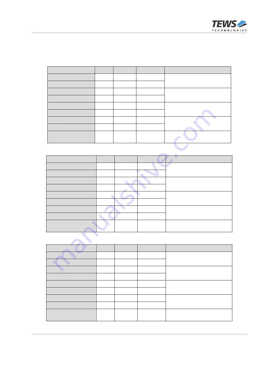
7.9.3 User FPGA Pinning
Each ADC is connected to the User FPGA (Kintex-7) via a dedicated serial clocked Interface. Each ADC
device has one input clock, one output clock and one conversion signal. For each ADC channel there is a
respective data output line, so both ADC channel transfers data at the same time.
Signal
Bank
VCCO
Pin
Description
12
2.5V
AF24
Differential Clock Output for
ADC Channel 1 and 2
SCK_00-
12
2.5V
AF25
SC
12
2.5V
Y23
Differential Clock Input for
ADC Channel 1 and 2
SCKOUT_00-
12
2.5V
AA24
12
2.5V
U24
Differential Data from ADC
Channel 1
SDO1_00-
12
2.5V
U25
12
2.5V
AD25
Differential Data from ADC
Channel 2
SDO2_00-
12
2.5V
AE25
CNV_N_00
12
2.5V
AB26
Convert Signal for ADC
Channel 1 and 2
Signal
Bank
VCCO
Pin
Description
13
2.5V
T24
Differential Clock Output for
ADC Channel 3 and 4
SCK_01-
13
2.5V
T25
SC
13
2.5V
R21
Differential Clock Input for
ADC Channel 3 and 4
SCKOUT_01-
13
2.5V
P21
13
2.5V
T20
Differential Data from ADC
Channel 3
SDO1_01-
13
2.5V
R20
13
2.5V
T22
Differential Data from ADC
Channel 4
SDO2_01-
13
2.5V
T23
CNV_N_01
13
2.5V
P19
Convert Signal for ADC
Channel 3 and 4
Signal
Bank
VCCO
Pin
Description
12
2.5V
AB21
Differential Clock Output for
ADC Channel 5 and 6
SCK_02-
12
2.5V
AC21
SC
12
2.5V
AC23
Differential Clock Input for
ADC Channel 5 and 6
SCKOUT_02-
12
2.5V
AC24
12
2.5V
V21
Differential Data from ADC
Channel 5
SDO1_02-
12
2.5V
W21
12
2.5V
AD21
Differential Data from ADC
Channel 6
SDO2_02-
12
2.5V
AE21
CNV_N_02
12
2.5V
Y26
Convert Signal for ADC
Channel 5 and 6


