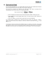
TPMC533 User Manual Issue 1.0.1
Page 96 of 107
8 Sequencer
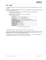
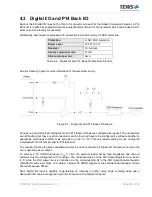
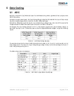
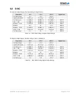
To be able to periodically sample analog values with ADCs or to periodically output analog values with
DACs, "Sequencers" can be used.
Each ADC may be assigned to the ADC Sequencer by configuring it to operate in Sequencer Mode in its
corresponding ADC Mode Register. Each DAC may be assigned to the DAC Sequencer by configuring it to
operate in Sequencer Mode in its corresponding DAC Mode Register.
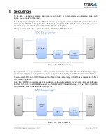
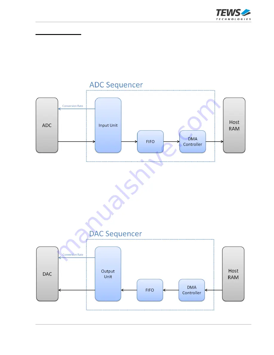
A Sequencer consists of an Input/Output Unit, a FIFO and a DMA Controller.
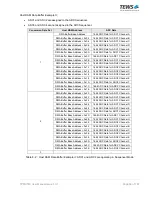
Figure 8-1 : ADC Sequencer
The Input Unit or Output Unit sets the Sequencer's Conversion Rate (the rate at which analog-to-digital
conversions or digital-to-analog conversions are performed) by selecting one of the two Conversion Clocks.
The on-board FIFOs buffer ADC Data and DAC Data to make sure delays in DMA bus accesses don’t affect
ADC or DAC operation.
Since the TPMC533 can produce/require quite large data volumes when converting at full speed, bulk data
transfers to/from the Host RAM Data Buffers are handled with PCI Bus DMA transfers. The TPMC533’s DMA
controllers use Block Transfer Mode DMA Cycles.
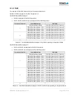
Figure 8-2 : DAC Sequencer


