TPMC533 User Manual Issue 1.0.1
Page 32 of 107
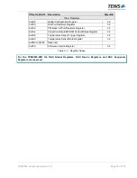
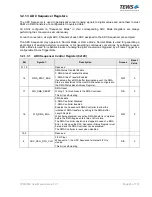
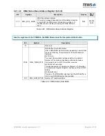
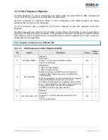
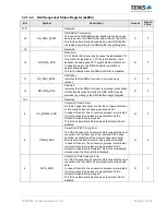
3.2.1.3.9
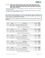
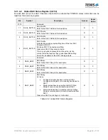
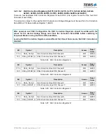
DMA Status Base Address Register (0x14C)
Bit
Symbol
Description
Access
Reset
Value
31:0
DMA_STAT_ADDR
DMA Status Base Address
PCI memory mapped base address of the address location
in Host RAM the DMA Status information is written to (if
enabled) as soon as the processing of a DMA Buffer is
done.
R/W
0x0000
0000
Table 3-29: DMA Status Base Address Register
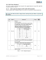
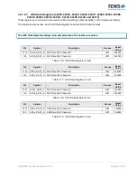
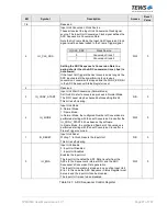
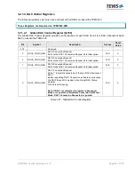
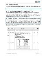
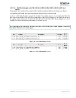
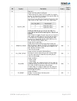
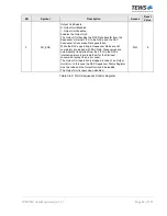
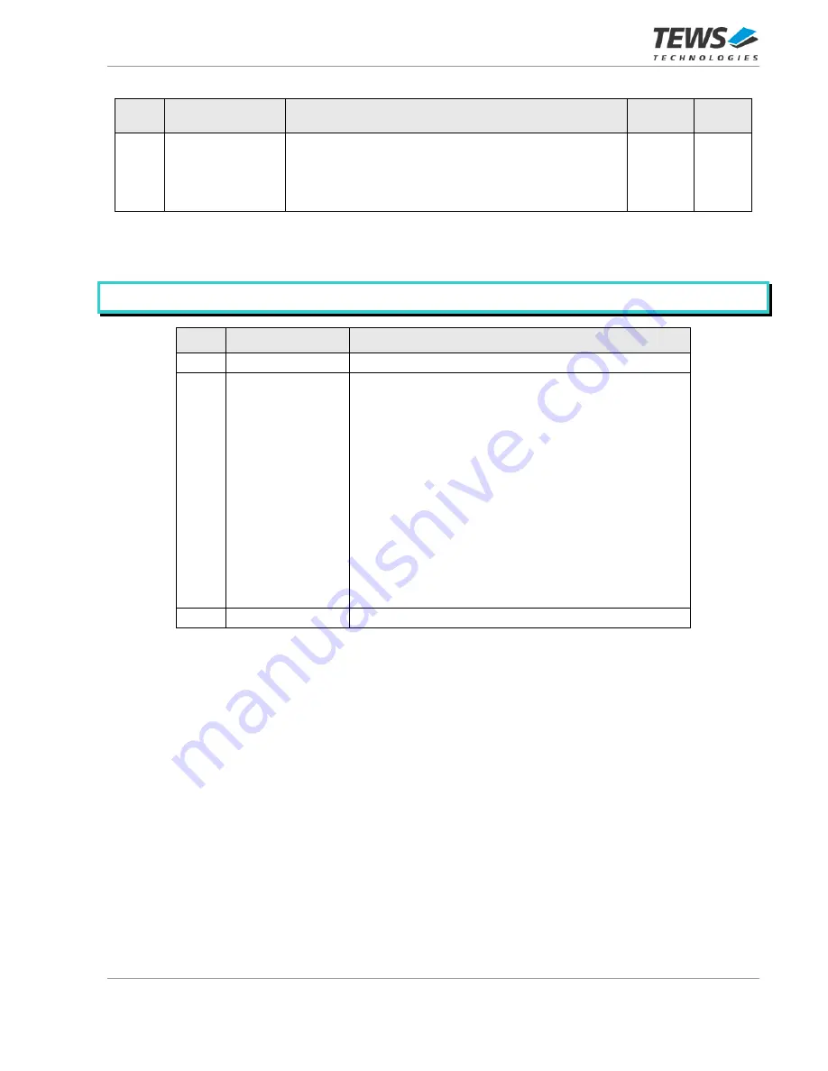
Like the registers of the TPMC533, the DMA Status must be interpreted Little Endian.
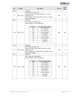
Bit
Symbol
Description
31
-
Reserved
30:28
DMA_TERM_STAT
DMA Buffer Termination Status
After a DMA Buffer was terminated, depending on which bits
are set in this array, the reason(s) for the termination are
indicated.
Bit 30: Error
The Input Unit operation is stopped before the desired
Number of Conversions has been performed because a
Conversion Error or a FIFO Overflow occurred.
Bit 29: Block/Frame End
The desired number of samples (configured in the Number
of Conversions Register Register) has been written to DMA
Buffers.
Bit 28: Buffer End
The end of the DMA Buffer was reached (the DMA Buffer is
full). A new DMA Buffer must be provided.
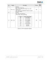
27:0
DMA_NUM_BYTES
Number of Transferred Bytes
Table 3-30: DMA Status (Host RAM)


