TPMC533 User Manual Issue 1.0.1
Page 47 of 107
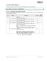
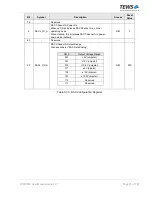
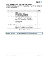
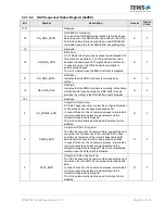
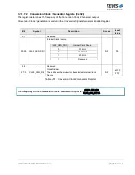
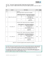
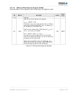
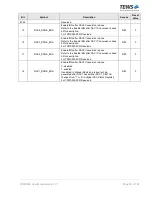
3.2.1.6.4
Conversion Count Register (0x2F8)
Bit
Symbol
Description
Access
Reset
Value
31:28
-
Reserved
-
-
27:0
DAC_SEQ_CONV_COUNT
Number of Conversions that have been performed
Normal Mode:
The value is automatically reset when the (next) Output
Unit Start Conversion is initiated in the DAC Sequencer
Control Register.
Frame Mode:
The value is automatically reset at a Frame Trigger event
(except for the case when an Output Unit Frame Error
occurred).
R
0x000
0000
Table 3-45: Conversion Count Register
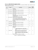
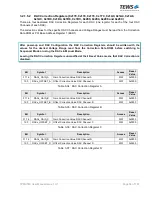
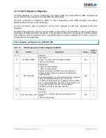
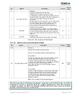
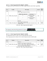
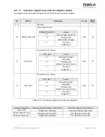
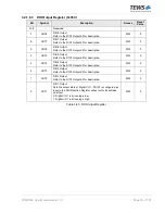
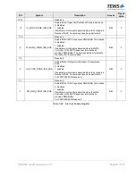
3.2.1.6.5
FIFO Level Register (0x2FC)
Bit
Symbol
Description
Access
Reset
Value
31:0
DAC_SEQ_FIFO_LEVEL
FIFO Level
This value shows the current fill level of the Sequencer's
internal FIFO. It is measured in number of bytes.
(a DAC Data value consists of two bytes)
R
0x0000
0000
Table 3-46: FIFO Level Register
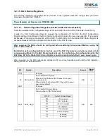
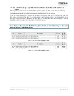
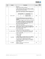
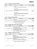
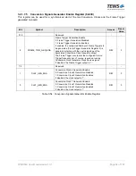
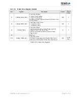
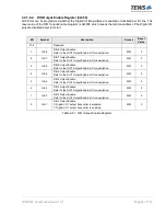
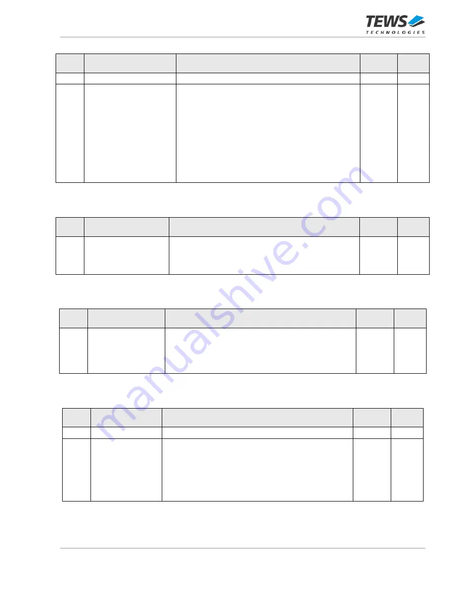
3.2.1.6.6
DMA Buffer Base Address Register (0x308)
Bit
Symbol
Description
Access
Reset
Value
31:0
RD_DMA_BUF_ADDR
DMA Buffer Base Address
PCI memory mapped base address of the DMA Buffer in
Host RAM that provides DAC Data.
The DMA Buffer Base Address is latched when the DMA
Buffer Length Register is written.
R/W
0x0000
0000
Table 3-47: DMA Buffer Base Address Register
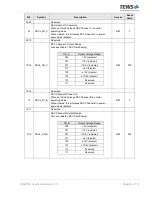
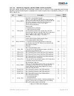
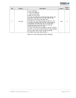
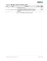
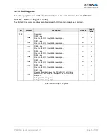
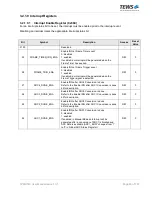
3.2.1.6.7
DMA Buffer Length Register (0x30C)
Bit
Symbol
Description
Access
Reset
Value
31:28
-
Reserved
-
-
27:0
RD_DMA_BUF_LEN
DMA Buffer Length
Byte Length of the provided DMA Buffer in Host RAM.
A write to the DMA Buffer Length Register initiates the
DMA transfer.
The Initiation of DMA transfers is only possible if
RD_DMA_IDLE in the DAC Sequencer Status Register is
‘1’.
R/W
0x0000
0000
Table 3-48: DMA Buffer Length Register


