background image


TPMC533 User Manual Issue 1.0.1 

Page 54 of 107 

3.2.1.7.7 

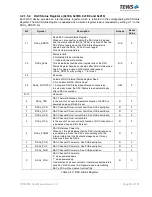
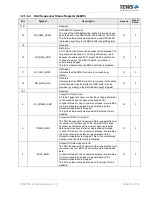
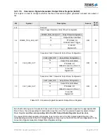
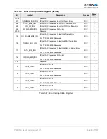
Conversion Signals Source Selection Register (0x344) 

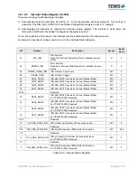
This register is used to select the signal source for the three Conversion Signals. 


Bit 

Symbol 

Description 

Access 

Reset 
Value 

31:6 

Reserved 

5:4 

FRAME_TRIG_SRC 

Frame Trigger Source 
 

FRAME_TRIG_SRC 

Source 

0x 

Frame Trigger Generator


10 

P14 Back I/O 

Global Frame Trigger


11 

Front I/O 

Digital I/O 5 


R/W 

00 

3:2 

CLK2_SRC 

Conversion Clock 2 Source 
 

CLK2_SRC 

Source 

0x 

Conversion Clock 2 

Generator


10 

P14 Back I/O 

Global Conversion Clock 2


11 

Front I/O 

Digital I/O 3 


R/W 

00 

1:0 

CLK1_SRC 

Conversion Clock 1 Source 
 

CLK1_SRC 

Source 

0x 

Conversion Clock 1 

Generator


10 

P14 Back I/O 

Global Conversion Clock 1


11 

Front I/O 

Digital I/O 1 


R/W 

00 

Table 3-56:  Conversion Signals Source Selection Register 


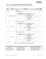
System Configuration 

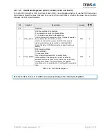
Conversion Signals Generator Output Driver 

Conversion Signals Source Selection 

Single Card 

Output Driver disabled


Conversion Signal Generators


Multiboard Master Card 

P14 Back I/O or Front I/O


P14 Back I/O or Front I/O


Multiboard Target Card 

Output Driver disabled 

P14 Back I/O or Front I/O 

Summary of Contents for TPMC533

Page 1: ...MC533 32x ADC 16x 0x DAC and 8x Digital I O Version 1 0 User Manual Issue 1 0 1 May 2018 TEWS TECHNOLOGIES GmbH Am Bahnhof 7 25469 Halstenbek Germany Phone 49 0 4101 4058 0 Fax 49 0 4101 4058 19 e mail info tews com www tews com ...

Page 2: ...HNOLOGIES GmbH has made any effort to ensure that this manual is accurate and complete However TEWS TECHNOLOGIES GmbH reserves the right to change the product described in this document at any time without notice TEWS TECHNOLOGIES GmbH is not liable for any damage arising out of the application or use of the device described herein Style Conventions Hexadecimal characters are specified with prefix...

Page 3: ...TPMC533 User Manual Issue 1 0 1 Page 3 of 107 Issue Description Date 1 0 0 Initial issue December 2017 1 0 1 Power Requirements revised May 2018 ...

Page 4: ... P14 Back I O 88 4 3 5 DATA CODING 89 ADC 89 5 1 DAC 90 5 2 6 CORRECTION DATA 91 7 OPERATING MODES 92 Manual Mode 92 7 1 7 1 1 DAC Immediate Conversion 92 7 1 2 DAC Controlled Conversion 92 Sequencer Mode 93 7 2 7 2 1 Normal Mode 94 7 2 2 Frame Mode 95 8 SEQUENCER 96 Host RAM Data Buffers 97 8 1 8 1 1 ADC 98 8 1 2 DAC 100 9 CONVERSION SIGNALS 101 Multi board Synchronization 103 9 1 10 PIN ASSIGNME...

Page 5: ...ES 19 TABLE 3 5 GLOBAL ADC CONTROL REGISTER 19 TABLE 3 6 GLOBAL ADC STATUS REGISTER 20 TABLE 3 7 ADC CONFIGURATION REGISTER 21 TABLE 3 8 ADC CORRECTION REGISTER A 22 TABLE 3 9 ADC CORRECTION REGISTER B 22 TABLE 3 10 ADC CORRECTION REGISTER C 22 TABLE 3 11 ADC CORRECTION REGISTER D 22 TABLE 3 12 ADC CORRECTION REGISTER E 22 TABLE 3 13 ADC CORRECTION REGISTER F 23 TABLE 3 14 ADC CORRECTION REGISTER ...

Page 6: ...5 CONVERSION COUNT REGISTER 47 TABLE 3 46 FIFO LEVEL REGISTER 47 TABLE 3 47 DMA BUFFER BASE ADDRESS REGISTER 47 TABLE 3 48 DMA BUFFER LENGTH REGISTER 47 TABLE 3 49 DMA BUFFER NEXT ADDRESS REGISTER 48 TABLE 3 50 CONVERSION CLOCK 1 GENERATOR REGISTER 49 TABLE 3 51 CONVERSION CLOCK 2 GENERATOR REGISTER 50 TABLE 3 52 FRAME TRIGGER GENERATOR REGISTER 1 51 TABLE 3 53 FRAME TRIGGER GENERATOR REGISTER 2 5...

Page 7: ...7 TABLE 4 4 DIGITAL I O AND P14 BACK I O ELECTRICAL INTERFACE 88 TABLE 5 1 ADC DATA CODING EXAMPLE 89 TABLE 5 2 ADC DATA CODING BIPOLAR INPUT RANGE 89 TABLE 5 3 DAC DATA CODING UNIPOLAR OUTPUT RANGE 90 TABLE 5 4 DAC DATA CODING BIPOLAR OUTPUT RANGE 90 TABLE 8 1 HOST RAM DATA BUFFER EXAMPLE I 98 TABLE 8 2 HOST RAM DATA BUFFER EXAMPLE II 99 TABLE 8 3 HOST RAM DATA BUFFER EXAMPLE I 100 TABLE 8 4 HOST...

Page 8: ... temperature dependent errors The TPMC533 provides two Sequencers one for AD Conversions and another one for DA Conversions To perform periodic simultaneous conversions the conversion rates are programmable and can be output to other modules on PMC Back I O Connector P14 or Front I O Connector DIO pins for synchronization purposes The TPMC533 can also operate as a target which means that the conve...

Page 9: ...TPMC533 User Manual Issue 1 0 1 Page 9 of 107 Figure 1 1 Block Diagram ...

Page 10: ...Kbit Serial EEPROM M93C86 W ST ADC Interface Number of ADC Channels 32 Input Type True bipolar differential Input Voltage Ranges 5V and 10V one common setting for all eight channels of each ADC Sample Rate 200kSPS DAC Interface Number of DAC Channels TPMC533 10R 16 TPMC533 20R 0 Output Type Unipolar bipolar single ended Output Voltage Ranges 5V 10V 10 8V 5V 10V and 10 8V individual setting for eac...

Page 11: ...BF values shown are based on calculation according to MIL HDBK 217F and MIL HDBK 217F Notice 2 Environment GB 20 C The MTBF calculation is based on component FIT rates provided by the component suppliers If FIT rates are not available MIL HDBK 217F and MIL HDBK 217F Notice 2 formulas are used for FIT rate calculation Humidity 5 95 non condensing Weight TPMC533 10R 72 8g TPMC533 20R 72 5g Table 2 1...

Page 12: ...33 10R 0x0014 TPMC533 20R Table 3 1 PCI Identifier PCI Base Address Register Configuration 3 2 The two address spaces on the TPMC533 are accessed from the PCI side by addressing two PCI Base Address Registers mapped in the PCI Memory Space PCI Base Address Register Offset in PCI Configuration Space PCI Space Mapping Size Byte Port Width Bit Endian Mode Description 0 0x10 MEM 1024 32 Little Registe...

Page 13: ...ster E 32 0x02C ADC1 Correction Register F 32 0x030 ADC1 Correction Register G 32 0x034 ADC1 Correction Register H 32 0x038 ADC1 Data Register A B 32 0x03C ADC1 Data Register C D 32 0x040 ADC1 Data Register E F 32 0x044 ADC1 Data Register G H 32 0x048 ADC1 Mode Register 32 0x04C Reserved 0x050 Reserved 0x054 ADC2 Configuration Register 32 0x058 Reserved 0x05C ADC2 Correction Register A 32 0x060 AD...

Page 14: ...2 0x0C0 ADC3 Data Register A B 32 0x0C4 ADC3 Data Register C D 32 0x0C8 ADC3 Data Register E F 32 0x0CC ADC3 Data Register G H 32 0x0D0 ADC3 Mode Register 32 0x0D4 Reserved 0x0D8 Reserved 0x0DC ADC4 Configuration Register 32 0x0E0 Reserved 0x0E4 ADC4 Correction Register A 32 0x0E8 ADC4 Correction Register B 32 0x0EC ADC4 Correction Register C 32 0x0F0 ADC4 Correction Register D 32 0x0F4 ADC4 Corre...

Page 15: ...ved DAC Global Registers 0x158 Global DAC Control Register 32 0x15C Global DAC Status Register 32 0x160 Reserved 0x164 Reserved DAC Device Registers 0x168 DAC1 Configuration Register 32 0x16C Reserved 0x170 DAC1 Correction Register A 32 0x174 DAC1 Correction Register B 32 0x178 DAC1 Correction Register C 32 0x17C DAC1 Correction Register D 32 0x180 DAC1 Data Register A B 32 0x184 DAC1 Data Registe...

Page 16: ...e Register 32 0x1F0 Reserved 0x1F4 Reserved 0x1F8 DAC4 Configuration Register 32 0x1FC Reserved 0x200 DAC4 Correction Register A 32 0x204 DAC4 Correction Register B 32 0x208 DAC4 Correction Register C 32 0x20C DAC4 Correction Register D 32 0x210 DAC4 Data Register A B 32 0x214 DAC4 Data Register C D 32 0x218 DAC4 Status Register 32 0x21C DAC4 Mode Register 32 0x220 Reserved 0x224 Reserved 0x228 to...

Page 17: ...Conversion Signals Generator Output Driver Register 32 0x344 Conversion Signals Source Selection Register 32 0x348 Frame Timer Register 32 0x34C Reserved 0x350 Reserved DIO Registers 0x354 DIO Input Register 32 0x358 DIO Input Filter Debounce Register 32 0x35C DIO Output Register 32 0x360 DIO Output Enable Register 32 0x364 Reserved 0x368 Reserved Interrupt Registers 0x36C Interrupt Enable Registe...

Page 18: ...x3A0 P14 Back I O Pull Resistors Register 32 0x3A4 Correction Data EEPROM Control Status Register 32 0x3A8 Temperature Sensor Trigger Register 32 0x3AC Temperature Sensor Data Register 32 0x3B0 to 0x3F8 Reserved 0x3FC Firmware Version Register 32 Table 3 3 Register Space For the TPMC533 20R the DAC Global Registers DAC Device Registers and DAC Sequencer Registers are reserved ...

Page 19: ...ster 0x000 The Global ADC Control Register provides control options for each ADC for all eight ADC Channels of each ADC on board the TPMC533 Bit Symbol Description Access Reset Value 31 4 Reserved 3 ADC4_CONV_REQ ADC4 Conversion Request Refer to the ADC1 Conversion Request bit for description R S 0 2 ADC3_CONV_REQ ADC3 Conversion Request Refer to the ADC1 Conversion Request bit for description R S...

Page 20: ...iption R 0 2 ADC3_BUSY ADC3 Busy Refer to the ADC1 Busy bit for description R 0 1 ADC2_BUSY ADC2 Busy Refer to the ADC1 Busy bit for description R 0 0 ADC1_BUSY ADC1 Busy Set when analog sampling is in progress data is transferred from the ADC If ADC1 Operating Mode is set to Manual Mode in the corresponding ADC Mode Register this bit is set by writing to ADC1_CONV_REQ in the Global ADC Control Re...

Page 21: ...ing is active the ADC takes multiple samples and averages them This improves the signal to noise ratio The ADCx_BUSY high time in the Global ADC Status Register is extended until all samples are taken Note If Oversampling is turned on the maximum AD Sample Rate of the ADC is less than 200kSPS OS Oversampling Ratio 000 No Oversampling 001 2 010 4 011 8 100 16 101 32 110 64 111 Not valid When changi...

Page 22: ...tion is disabled Bit Symbol Description Access Reset Value 31 16 ADCx_GAIN_A Gain Correction Value ADC Channel A R W 0x0000 15 0 ADCx_OFFSET_A Offset Correction Value ADC Channel A R W 0x0000 Table 3 8 ADC Correction Register A Bit Symbol Description Access Reset Value 31 16 ADCx_GAIN_B Gain Correction Value ADC Channel B R W 0x0000 15 0 ADCx_OFFSET_B Offset Correction Value ADC Channel B R W 0x00...

Page 23: ...rection Register F Bit Symbol Description Access Reset Value 31 16 ADCx_GAIN_G Gain Correction Value ADC Channel G R W 0x0000 15 0 ADCx_OFFSET_G Offset Correction Value ADC Channel G R W 0x0000 Table 3 14 ADC Correction Register G Bit Symbol Description Access Reset Value 31 16 ADCx_GAIN_H Gain Correction Value ADC Channel H R W 0x0000 15 0 ADCx_OFFSET_H Offset Correction Value ADC Channel H R W 0...

Page 24: ...1 16 ADCx_DATA_B ADC Data ADC Channel B R W 0x0000 15 0 ADCx_DATA_A ADC Data ADC Channel A R W 0x0000 Table 3 16 ADC Data Register A B Bit Symbol Description Access Reset Value 31 16 ADCx_DATA_D ADC Data ADC Channel D R W 0x0000 15 0 ADCx_DATA_C ADC Data ADC Channel C R W 0x0000 Table 3 17 ADC Data Register C D Bit Symbol Description Access Reset Value 31 16 ADCx_DATA_F ADC Data ADC Channel F R W ...

Page 25: ...from ADC Data Registers Bit Symbol Description Access Reset Value 31 1 Reserved 0 ADCx_MODE ADC Operating Mode 0 Manual Mode 1 Sequencer Mode This bit sets the general ADC Operating Mode In Manual Mode analog sampling is requested by software commands there is no periodic conversion rate In Sequencer Mode analog inputs are sampling periodically at a configurable conversion rate R W 0 Table 3 20 AD...

Page 26: ...bol Description Access Reset Value 31 19 Reserved 18 DMA_STAT_ENA DMA Status Transfer Enable 0 DMA Status Transfer Disabled 1 DMA Status Transfer Enabled If enabled after a DMA Buffer termination event the DMA Status is transferred to the Host RAM location configured in the DMA Status Base Address Register R W 0 17 WR_DMA_RESET DMA Reset Writing 1 to this bit resets the DMA Controller This bit is ...

Page 27: ...is bit to start a conversion process in Normal Mode The FIFO Level may be checked before setting this bit This bit is self clearing R S 0 2 IU_MODE Input Unit Mode 0 Normal Mode 1 Frame Mode In Normal Mode the configured Number of Conversions is performed starting with the next Conversion Clock after the IU_CONV_START bit has been set by software In Frame Mode the configured Number of Conversions ...

Page 28: ...d number of samples configured in the Number of Conversions Register has been written to DMA Buffers Bit 20 Buffer End The end of the DMA Buffer was reached the DMA Buffer is full A new DMA Buffer must be provided R 000 19 Reserved 18 WR_DMA_ERR DMA Error A PCI Master Abort occurred because the addressed PCI Target did not respond or a PCI Target Abort occurred because the addressed PCI Target det...

Page 29: ...ed R 0 4 FIFO_OF Input Unit FIFO Overflow Error The Input Unit wants to write sampled values from the ADCs to the FIFO but the FIFO is full because AD samples could not be written to Host RAM fast enough In case of this error the conversion process is terminated no more conversion pulses are generated and the Input Unit operation is stopped This bit is automatically cleared when the Input Unit is ...

Page 30: ...Conversions per frame has been performed the conversion process is stopped until the next Frame Trigger event occurs and the IU_CONV_ACTIVE bit in the ADC Sequencer Status Register is cleared R W 0x000 0000 Table 3 23 Number of Conversions Register Note that every time the ADC Sequencer triggers a conversion all eight ADC Channels of all ADCs configured to operate in Sequencer Mode are updated sim...

Page 31: ...s written R W 0x0000 0000 Table 3 26 DMA Buffer Base Address Register 3 2 1 3 7 DMA Buffer Length Register 0x144 Bit Symbol Description Access Reset Value 31 28 Reserved 27 0 WR_DMA_BUF_LEN DMA Buffer Length Byte Length of the provided DMA Buffer in Host RAM A write to the DMA Buffer Length Register initiates the DMA transfer The Initiation of DMA transfers is only possible if WR_DMA_IDLE in the A...

Page 32: ...bol Description 31 Reserved 30 28 DMA_TERM_STAT DMA Buffer Termination Status After a DMA Buffer was terminated depending on which bits are set in this array the reason s for the termination are indicated Bit 30 Error The Input Unit operation is stopped before the desired Number of Conversions has been performed because a Conversion Error or a FIFO Overflow occurred Bit 29 Block Frame End The desi...

Page 33: ...Conversion Request bit for description R S 0 2 DAC3_CONV_REQ DAC3 Conversion Request Refer to the DAC1 Conversion Request bit for description R S 0 1 DAC2_CONV_REQ DAC2 Conversion Request Refer to the DAC1 Conversion Request bit for description R S 0 0 DAC1_CONV_REQ DAC1 Conversion Request Write 1 to start the conversion of the four DAC Channels of DAC1 Before requesting DAC1 Conversion software s...

Page 34: ... Clear when DAC1 Channels are stable This is no physical representation of any kind just an internal timer that expires 10µs typical specified settling time after an update of the DAC1 analog outputs R 0 7 4 Reserved 3 DAC4_BUSY DAC4 Busy Refer to the DAC1 Busy bit for description R 0 2 DAC3_BUSY DAC3 Busy Refer to the DAC1 Busy bit for description R 0 1 DAC2_BUSY DAC2 Busy Refer to the DAC1 Busy ...

Page 35: ...power up the DACs should be configured before switching to Sequencer Mode or using the DACs in Manual Mode Each DAC must be configured before it can be used The DAC Channels can only be used when their corresponding PUx bit in the DAC Status Register is set For verification after configuration write the DAC Busy Bit in the Global DAC Status Register should be monitored whether it was cleared again...

Page 36: ...tage Range 000 5V unipolar 001 10V unipolar 010 10 8V unipolar 011 5V bipolar 100 10V bipolar 101 10 8V bipolar 110 Reserved 111 Reserved R W 000 15 14 Reserved 13 DACx_PU_B DAC Channel B Power Up When set this bit places DAC Channel B in normal operating mode When cleared this bit places DAC Channel B in power down mode default R W 0 12 11 Reserved 10 8 DACx_OR_B DAC Channel B Output Range Also s...

Page 37: ...ormal operating mode When cleared this bit places DAC Channel A in power down mode default R W 0 4 3 Reserved 2 0 DACx_OR_A DAC Channel A Output Range Also see chapter DAC Data Coding OR_A Output Voltage Range 000 5V unipolar 001 10V unipolar 010 10 8V unipolar 011 5V bipolar 100 10V bipolar 101 10 8V bipolar 110 Reserved 111 Reserved R W 000 Table 3 33 DAC Configuration Register ...

Page 38: ...rs unmodified at their Reset Value means that DAC Correction is disabled Bit Symbol Description Access Reset Value 31 16 DACx_GAIN_A Gain Correction Value DAC Channel A R W 0x0000 15 0 DACx_OFFSET_A Offset Correction Value DAC Channel A R W 0x0000 Table 3 34 DAC Correction Register A Bit Symbol Description Access Reset Value 31 16 DACx_GAIN_B Gain Correction Value DAC Channel B R W 0x0000 15 0 DAC...

Page 39: ... If not already set because of ongoing communication with the DAC the DAC Busy bit in the Global DAC Status Register is set and remains set until the configuration data transfer to the DAC is done For verification after data write the DAC Busy Bit in the Global DAC Status Register should be monitored whether it was cleared again Bit Symbol Description Access Reset Value 31 16 DACx_DATA_B DAC Data ...

Page 40: ...Status Read after each conversion In automatic mode the DAC Status is read automatically after a DAC conversion R W 0 27 10 Reserved 9 DACx_TSD DAC Thermal Shutdown Alert In the event of an over temperature situation the DAC is powered down and this bit is set R 0 8 DACx_OCD DAC Channel D Over current Alert See OCA description R 0 7 DACx_OCC DAC Channel C Over current Alert See OCA description R 0...

Page 41: ... Mode If set to Immediate Conversion a DAC Channel is updated immediately after a DAC Data transfer If set to Controlled Conversion the DAC Channels are updated simultaneously by a write to the Global DAC Control Register DAC Data must have been transferred before R W 0 0 DACx_MODE DAC Operating Mode 0 Manual Mode 1 Sequencer Mode This bit sets the general DAC Operating Mode In Manual Mode the ana...

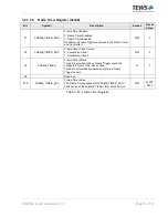
Page 42: ...red by a Frame Trigger at a configurable Frame Trigger Rate These Registers are Reserved on TPMC533 20R 3 2 1 6 1 DAC Sequencer Control Register 0x2E8 Bit Symbol Description Access Reset Value 31 18 Reserved 17 RD_DMA_RESET DMA Reset Writing 1 to this bit resets the DMA Controller This bit is self clearing R S 0 16 RD_DMA_ENA DMA Enable 0 DMA Controller Disabled 1 DMA Controller Enabled Enables th...

Page 43: ...e OU_CONV_ERR bit in the DAC Sequencer Status Register is set R W 0 4 PRELOAD_CLEAR Output Unit Pre Load Clear Setting this bit marks the DACs operating in Sequencer Mode as being un loaded The DACs are automatically pre loaded again when DAC Data is becomes available in the DAC Sequencer s internal FIFO This bit is self clearing R S 0 3 OU_CONV_START Output Unit Start Conversion Normal Mode Set t...

Page 44: ... Rate generation While the DACs operating in Sequencer Mode are not completely pre loaded with DAC Data these values are automatically transferred from the FIFO to the DACs internal registers to pre load them for the first next conversion except in an error case The Output Unit operation is stopped in case of an Output Unit Error In this case the DAC Sequencer Status Register must be read and the ...

Page 45: ...egister R 0 15 7 Reserved 6 OU_FRAME_ERR Output Unit Frame Error A Frame Trigger event occurs but the configured Number of Conversions has not been processed so far In case of this error the conversion process is terminated no more conversion pulses are generated and the Output Unit operation is stopped This bit is automatically cleared when the Output Unit is disabled R 0 5 TIMING_ERR Output Unit...

Page 46: ... of Conversions Register 0x2F4 Bit Symbol Description Access Reset Value 31 28 Reserved 27 0 DAC_SEQ_NUM_CONV Number of Conversions to be performed Set to 0 for continuous digital to analog conversions Normal Mode Number of conversions after OU_CONV_START was set per requested block of digital to analog conversions When the configured Number of Conversions has been performed the conversion process...

Page 47: ...ernal FIFO It is measured in number of bytes a DAC Data value consists of two bytes R 0x0000 0000 Table 3 46 FIFO Level Register 3 2 1 6 6 DMA Buffer Base Address Register 0x308 Bit Symbol Description Access Reset Value 31 0 RD_DMA_BUF_ADDR DMA Buffer Base Address PCI memory mapped base address of the DMA Buffer in Host RAM that provides DAC Data The DMA Buffer Base Address is latched when the DMA...

Page 48: ...ption Access Reset Value 31 0 RD_DMA_NEXT_ADDR DMA Buffer Next Address This register holds the PCI address of the address location in Host RAM the next DAC Data is read from It can be used to determine how much information is left in the provided DMA Buffer R 0x0000 0000 Table 3 49 DMA Buffer Next Address Register ...

Page 49: ...ion Clock 1 generation is started in the Conversion Signals Generator Enable Register Bit Symbol Description Access Reset Value 31 Reserved 30 29 CLK1_GEN_SRC Internal Clock Source CLK1_GEN_SRC Internal Clock Source 00 20 MHz 01 22 05 MHz 10 60 MHz 11 Reserved R W 00 28 Reserved 27 0 CLK1_GEN_DIV Clock Divider These bits set the divider for the selected Internal Clock Source R W 0xFFF FFFF Table 3...

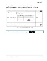
Page 50: ... Enable Register Bit Symbol Description Access Reset Value 31 Reserved 30 29 CLK2_GEN_SRC Internal Clock Source CLK2_GEN_SRC Internal Clock Source 00 20 MHz 01 22 05 MHz 10 60 MHz 11 Reserved R W 00 28 Reserved 27 0 CLK2_GEN_DIV Clock Divider These bits set the divider for the selected Internal Clock Source R W 0xFFF FFFF Table 3 51 Conversion Clock 2 Generator Register The frequency of the Conver...

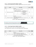
Page 51: ...version Clock Generator output R W 0xFFF FFFF Table 3 52 Frame Trigger Generator Register 1 The frequency of the Frame Trigger Generator output is FRAME_TRIG_GEN_SRC FRAME_TRIG_GEN_DIV 1 3 2 1 7 4 Frame Trigger Generator Register 2 0x330 This register determines the number of Frame Triggers generated on board Frame Trigger generation is started in the Conversion Signals Generator Enable Register B...

Page 52: ...is generated starting with the next rising edge of the associated Conversion Clock Generator output The Frame Trigger is output at the configured Frame Trigger frequency but of course requires a running Conversion Clock Generator Clock Source signal If disabled the Frame Trigger output is 1 R W 0 7 2 Reserved 1 CLK2_GEN_ENA Conversion Clock 2 Generation Enable 0 Conversion Clock 2 Generation Disab...

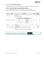
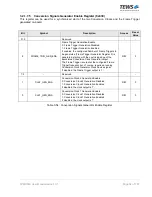
Page 53: ... 11 Front I O Digital I O 3 R W 00 1 0 CLK1_GEN_OUT Conversion Clock 1 Generator Output Driver Configuration CLK1_GEN_OUT Output Driver Configuration 0x Output Driver disabled 10 P14 Back I O Global Conversion Clock 1 11 Front I O Digital I O 1 R W 00 Table 3 55 Conversion Signals Generator Output Driver Register Note that for driving out a Conversion Clock and or Frame Trigger generator signal on...

Page 54: ...2_SRC Source 0x Conversion Clock 2 Generator 10 P14 Back I O Global Conversion Clock 2 11 Front I O Digital I O 3 R W 00 1 0 CLK1_SRC Conversion Clock 1 Source CLK1_SRC Source 0x Conversion Clock 1 Generator 10 P14 Back I O Global Conversion Clock 1 11 Front I O Digital I O 1 R W 00 Table 3 56 Conversion Signals Source Selection Register System Configuration Conversion Signals Generator Output Dri...

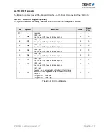
Page 55: ...0 30 FRAME_TIMER_SRC Frame Timer Clock Source 0 Conversion Clock 1 1 Conversion Clock 2 R W 0 29 FRAME_TIMER Frame Timer Status This bit is set when after a Frame Trigger event the configured Frame Timer has expired This bit is automatically cleared every time a Frame Trigger occurs R 0 28 Reserved 27 0 FRAME_TIMER_VAL Frame Timer Value The Frame Timer expires after FRAME_TIMER_VAL 1 clock cycles ...

Page 56: ...DIO7 Input Refer to the DIO1 Input bit for description R 0 5 IN6 DIO6 Input Refer to the DIO1 Input bit for description R 0 4 IN5 DIO5 Input Refer to the DIO1 Input bit for description R 0 3 IN4 DIO4 Input Refer to the DIO1 Input bit for description R 0 2 IN3 DIO3 Input Refer to the DIO1 Input bit for description R 0 1 IN2 DIO2 Input Refer to the DIO1 Input bit for description R 0 0 IN1 DIO1 Input...

Page 57: ...duration smaller than TREJECT are filtered and are not passed on to the internal logic Please note that pulses with a duration between TPASS and TREJECT may or may not be filtered TPASS DEB 1 75ns 1 5 TREJECT The pass time can be configured from 75ns to 4 9152ms Pulses with a duration greater than TPASS are not filtered and are passed on to the internal logic After an input pin performs a rising o...

Page 58: ...0 4 OUT5 DIO5 Output Refer to the DIO1 Output bit for description R W 0 3 OUT4 DIO4 Output Refer to the DIO1 Output bit for description R W 0 2 OUT3 DIO3 Output Refer to the DIO1 Output bit for description R W 0 1 OUT2 DIO2 Output Refer to the DIO1 Output bit for description R W 0 0 OUT1 DIO1 Output Sets the output state of Digital I O 1 If DIO1 is configured as input in the DIO Direction Register...

Page 59: ...tion R W 0 6 OE7 DIO7 Output Enable Refer to the DIO1 Output Enable bit for description R W 0 5 OE6 DIO6 Output Enable Refer to the DIO1 Output Enable bit for description R W 0 4 OE5 DIO5 Output Enable Refer to the DIO1 Output Enable bit for description R W 0 3 OE4 DIO4 Output Enable Refer to the DIO1 Output Enable bit for description R W 0 2 OE3 DIO3 Output Enable Refer to the DIO1 Output Enable ...

Page 60: ...If enabled an interrupt will be generated when the Frame Trigger signal is detected R W 0 27 ADC4_DONE_ENA Enable IRQ after ADC4 Conversion is done Refer to the Enable IRQ after ADC1 Conversion is done bit for description R W 0 26 ADC3_DONE_ENA Enable IRQ after ADC3 Conversion is done Refer to the Enable IRQ after ADC1 Conversion is done bit for description R W 0 25 ADC2_DONE_ENA Enable IRQ after ...

Page 61: ...one Refer to the Enable IRQ after DAC1 Conversion is done bit for description For TPMC533 20R Reserved R W 0 17 DAC2_DONE_ENA Enable IRQ after DAC2 Conversion is done Refer to the Enable IRQ after DAC1 Conversion is done bit for description For TPMC533 20R Reserved R W 0 16 DAC1_DONE_ENA Enable IRQ after DAC1 Conversion is done 0 disabled 1 enabled If enabled in Manual Mode an interrupt will be ge...

Page 62: ...ntroller of the ADC Sequencer terminates its provided DMA Buffer The interrupt status bits indicate the reason for the termination R W 0 7 5 Reserved 4 OU_CONV_DONE_IRQ_ENA Enable IRQ at Output Unit Number of Conversions done 0 disabled 1 enabled If enabled an interrupt is asserted when the configured Number of DAC Conversions have been performed For TPMC533 20R Reserved R W 0 3 1 Reserved 0 RD_DM...

Page 63: ...f enabled an interrupt is asserted when the Sequencer Conversion Clock Source requests the next conversion but the ADCs are still busy performing the conversion process of the previous conversion R W 0 25 FIFO_OF_IRQ_ENA Enable IRQ at ADC Sequencer Input Unit FIFO Overflow Error 0 disabled 1 enabled If enabled an interrupt is asserted when the Input Unit wants to write sampled values from the ADCs...

Page 64: ...f enabled an interrupt is asserted when the DAC Sequencer s Conversion Rate requests the next conversion but at least one of the involved DACs is still busy For TPMC533 20R Reserved R W 0 17 DATA_ERR_IRQ_ENA Enable IRQ at DAC Sequencer Output Unit Data Underrun Error 0 disabled 1 enabled If enabled an interrupt is asserted when the Output Unit wants to perform a DAC Conversion but the DAC channels...

Page 65: ...to the Enable IRQ at DAC1 Alert bit for description For TPMC533 20R Reserved R W 0 1 DAC2_ALERT_ENA Enable IRQ at DAC2 Alert Refer to the Enable IRQ at DAC1 Alert bit for description For TPMC533 20R Reserved R W 0 0 DAC1_ALERT_ENA Enable IRQ at DAC1 Alert 0 disabled 1 enabled If enabled an interrupt is asserted when the DAC1 status is read and any of the over current bits or the thermal shutdown b...

Page 66: ... bit for description R W 0 4 DIO5_RISE Enable IRQ at DIO 5 Rising Edge See the Enable IRQ at DIO 1 Rising Edge bit for description R W 0 3 DIO4_RISE Enable IRQ at DIO 4 Rising Edge See the Enable IRQ at DIO 1 Rising Edge bit for description R W 0 2 DIO3_RISE Enable IRQ at DIO 3 Rising Edge See the Enable IRQ at DIO 1 Rising Edge bit for description R W 0 1 DIO2_RISE Enable IRQ at DIO 2 Rising Edge...

Page 67: ...it for description R W 0 4 DIO5_FALL Enable IRQ at DIO 5 Falling Edge See the Enable IRQ at DIO 1 Falling Edge bit for description R W 0 3 DIO4_FALL Enable IRQ at DIO 4 Falling Edge See the Enable IRQ at DIO 1 Falling Edge bit for description R W 0 2 DIO3_FALL Enable IRQ at DIO 3 Falling Edge See the Enable IRQ at DIO 1 Falling Edge bit for description R W 0 1 DIO2_FALL Enable IRQ at DIO 2 Falling...

Page 68: ...IRQ at Frame Timer event R C 0 28 FRAME_TRIG IRQ at Frame Trigger R C 0 27 ADC4_DONE IRQ after ADC4 Conversion is done Manual Mode R C 0 26 ADC3_DONE IRQ after ADC3 Conversion is done Manual Mode R C 0 25 ADC2_DONE IRQ after ADC2 Conversion is done Manual Mode R C 0 24 ADC1_DONE IRQ after ADC1 Conversion is done Manual Mode R C 0 23 20 Reserved 19 DAC4_DONE IRQ after DAC4 Conversion is done Manual...

Page 69: ...RQ at DAC Sequencer Output Unit Frame Error For TPMC533 20R Reserved R C 0 18 TIMING_ERR_IRQ IRQ at DAC Sequencer Output Unit DAC Timing Error For TPMC533 20R Reserved R C 0 17 DATA_ERR_IRQ IRQ at DAC Sequencer Output Unit Data Underrun Error For TPMC533 20R Reserved R C 0 16 RD_DMA_ERR_IRQ IRQ at DAC Sequencer DMA Error For TPMC533 20R Reserved R C 0 15 4 Reserved 3 DAC4_ALERT IRQ at DAC4 Alert F...

Page 70: ... 4 DIO5 IRQ at Digital I O 5 Refer to the IRQ at Digital I O 1 bit for description R C 0 3 DIO4 IRQ at Digital I O 4 Refer to the IRQ at Digital I O 1 bit for description R C 0 2 DIO3 IRQ at Digital I O 3 Refer to the IRQ at Digital I O 1 bit for description R C 0 1 DIO2 IRQ at Digital I O 2 Refer to the IRQ at Digital I O 1 bit for description R C 0 0 DIO1 IRQ at Digital I O 1 Indicates a rising ...

Page 71: ...ed by writing 1 to the appropriate bit in the Interrupt Status Register 1 Interrupts are cleared when the Interrupt Status Register is read R W 0 0 DMA_ENDIAN_CONF DMA Endian Configuration Sets the Endian Mode for DMA access to Host RAM 0 Little Endian Mode 16bit digital values are stored in Little Endian format in Host RAM 1 Big Endian Mode 16bit digital values are stored in Big Endian format in ...

Page 72: ...hat the default configuration for the Digital I O Pull Resistors is floating 3 2 1 10 3 P14 Back I O Pull Resistors Register 0x3A0 All P14 Back I O Signals Global Conversion Clock 1 Global Conversion Clock 2 and Global Frame Trigger are connected to 4 7kΩ pull resistors The voltage the pull resistors are connected to is programmable and can be configured to 3 3V 5V GND or floating level Bit Symbol...

Page 73: ...om the EEPROM Software should check that the EEBSY bit is 0 before reading data from the Correction Data ROM space R 0 15 0 EELOCK Correction Data EEPROM Lock This nibble must be set to the value 0xABCD to allow write accesses to the Correction Data ROM Writes to the Correction Data ROM are ignored while this nibble is not 0xABCD When the value of this nibble is changed from 0xABCD to a different ...

Page 74: ...utomatically when the data is valid in the Temperature Sensor Data Register R S 0 Table 3 73 Temperature Sensor Trigger Register 3 2 1 10 6 Temperature Sensor Data Register 0x3AC This register holds the measured 13bit two s complement data of the on board SE95 temperature sensor Bit Symbol Description Access Reset Value 31 0 TEMP Measured data of the on board temperature sensor The measured value ...

Page 75: ... Status Register can be polled Offset to BAR1 Description Size Bit Input Voltage Range 5 V 0x000 ADC1 Channel A OffsetCORR 16 0x002 ADC1 Channel A GainCORR 16 0x004 ADC1 Channel B OffsetCORR 16 0x006 ADC1 Channel B GainCORR 16 0x008 ADC1 Channel C OffsetCORR 16 0x00A ADC1 Channel C GainCORR 16 0x00C ADC1 Channel D OffsetCORR 16 0x00E ADC1 Channel D GainCORR 16 0x010 ADC1 Channel E OffsetCORR 16 0x...

Page 76: ...CORR 16 0x052 ADC3 Channel E GainCORR 16 0x054 ADC3 Channel F OffsetCORR 16 0x056 ADC3 Channel F GainCORR 16 0x058 ADC3 Channel G OffsetCORR 16 0x05A ADC3 Channel G GainCORR 16 0x05C ADC3 Channel H OffsetCORR 16 0x05E ADC3 Channel H GainCORR 16 0x060 ADC4 Channel A OffsetCORR 16 0x062 ADC4 Channel A GainCORR 16 0x064 ADC4 Channel B OffsetCORR 16 0x066 ADC4 Channel B GainCORR 16 0x068 ADC4 Channel ...

Page 77: ...16 0x09E ADC1 Channel H GainCORR 16 0x0A0 ADC2 Channel A OffsetCORR 16 0x0A2 ADC2 Channel A GainCORR 16 0x0A4 ADC2 Channel B OffsetCORR 16 0x0A6 ADC2 Channel B GainCORR 16 0x0A8 ADC2 Channel C OffsetCORR 16 0x0AA ADC2 Channel C GainCORR 16 0x0AC ADC2 Channel D OffsetCORR 16 0x0AE ADC2 Channel D GainCORR 16 0x0B0 ADC2 Channel E OffsetCORR 16 0x0B2 ADC2 Channel E GainCORR 16 0x0B4 ADC2 Channel F Off...

Page 78: ... Channel H GainCORR 16 0x0E0 ADC4 Channel A OffsetCORR 16 0x0E2 ADC4 Channel A GainCORR 16 0x0E4 ADC4 Channel B OffsetCORR 16 0x0E6 ADC4 Channel B GainCORR 16 0x0E8 ADC4 Channel C OffsetCORR 16 0x0EA ADC4 Channel C GainCORR 16 0x0EC ADC4 Channel D OffsetCORR 16 0x0EE ADC4 Channel D GainCORR 16 0x0F0 ADC4 Channel E OffsetCORR 16 0x0F2 ADC4 Channel E GainCORR 16 0x0F4 ADC4 Channel F OffsetCORR 16 0x...

Page 79: ...ORR 16 0x118 DAC2 Channel C OffsetCORR 16 0x11A DAC2 Channel C GainCORR 16 0x11C DAC2 Channel D OffsetCORR 16 0x11E DAC2 Channel D GainCORR 16 0x120 DAC3 Channel A OffsetCORR 16 0x122 DAC3 Channel A GainCORR 16 0x124 DAC3 Channel B OffsetCORR 16 0x126 DAC3 Channel B GainCORR 16 0x128 DAC3 Channel C OffsetCORR 16 0x12A DAC3 Channel C GainCORR 16 0x12C DAC3 Channel D OffsetCORR 16 0x12E DAC3 Channel...

Page 80: ...CORR 16 0x198 DAC2 Channel C OffsetCORR 16 0x19A DAC2 Channel C GainCORR 16 0x19C DAC2 Channel D OffsetCORR 16 0x19E DAC2 Channel D GainCORR 16 0x1A0 DAC3 Channel A OffsetCORR 16 0x1A2 DAC3 Channel A GainCORR 16 0x1A4 DAC3 Channel B OffsetCORR 16 0x1A6 DAC3 Channel B GainCORR 16 0x1A8 DAC3 Channel C OffsetCORR 16 0x1AA DAC3 Channel C GainCORR 16 0x1AC DAC3 Channel D OffsetCORR 16 0x1AE DAC3 Channe...

Page 81: ...nCORR 16 0x218 DAC2 Channel C OffsetCORR 16 0x21A DAC2 Channel C GainCORR 16 0x21C DAC2 Channel D OffsetCORR 16 0x21E DAC2 Channel D GainCORR 16 0x220 DAC3 Channel A OffsetCORR 16 0x222 DAC3 Channel A GainCORR 16 0x224 DAC3 Channel B OffsetCORR 16 0x226 DAC3 Channel B GainCORR 16 0x228 DAC3 Channel C OffsetCORR 16 0x22A DAC3 Channel C GainCORR 16 0x22C DAC3 Channel D OffsetCORR 16 0x22E DAC3 Chann...

Page 82: ...ORR 16 0x298 DAC2 Channel C OffsetCORR 16 0x29A DAC2 Channel C GainCORR 16 0x29C DAC2 Channel D OffsetCORR 16 0x29E DAC2 Channel D GainCORR 16 0x2A0 DAC3 Channel A OffsetCORR 16 0x2A2 DAC3 Channel A GainCORR 16 0x2A4 DAC3 Channel B OffsetCORR 16 0x2A6 DAC3 Channel B GainCORR 16 0x2A8 DAC3 Channel C OffsetCORR 16 0x2AA DAC3 Channel C GainCORR 16 0x2AC DAC3 Channel D OffsetCORR 16 0x2AE DAC3 Channel...

Page 83: ...CORR 16 0x318 DAC2 Channel C OffsetCORR 16 0x31A DAC2 Channel C GainCORR 16 0x31C DAC2 Channel D OffsetCORR 16 0x31E DAC2 Channel D GainCORR 16 0x320 DAC3 Channel A OffsetCORR 16 0x322 DAC3 Channel A GainCORR 16 0x324 DAC3 Channel B OffsetCORR 16 0x326 DAC3 Channel B GainCORR 16 0x328 DAC3 Channel C OffsetCORR 16 0x32A DAC3 Channel C GainCORR 16 0x32C DAC3 Channel D OffsetCORR 16 0x32E DAC3 Channe...

Page 84: ...nCORR 16 0x398 DAC2 Channel C OffsetCORR 16 0x39A DAC2 Channel C GainCORR 16 0x39C DAC2 Channel D OffsetCORR 16 0x39E DAC2 Channel D GainCORR 16 0x3A0 DAC3 Channel A OffsetCORR 16 0x3A2 DAC3 Channel A GainCORR 16 0x3A4 DAC3 Channel B OffsetCORR 16 0x3A6 DAC3 Channel B GainCORR 16 0x3A8 DAC3 Channel C OffsetCORR 16 0x3AA DAC3 Channel C GainCORR 16 0x3AC DAC3 Channel D OffsetCORR 16 0x3AE DAC3 Chann...

Page 85: ... 1 Page 85 of 107 Offset to BAR1 Description Size Bit Serial Number 0x7FC Serial Number High Word 16 0x7FE Serial Number Low Word 16 Table 3 76 Correction Data ROM For the TPMC533 20R the correction values for the DACs are reserved ...

Page 86: ...ction 7kV ESD rating 16 5V Overvoltage Clamp Protection Input Type True bipolar differential Input Impedance 1MΩ Input Capacitance 5pF Maximum Ground related Input Voltage 5V and 10V Full Scale Range 10V and 20V Common Mode Input Range 4V Sample Rate 200kSPS Table 4 1 ADC Electrical Interface Differential with Ground Reference Differential without Ground Reference Table 4 2 ADC Input Schemes If si...

Page 87: ...t limit Output Type unipolar bipolar single ended Output Voltage Ranges 5V 10V 10 8V 5V 10V and 10 8V DC Output Impedance 0 5Ω Maximum Load 2kΩ Capacitive Load 4000pF Settling Time 10µs Table 4 3 DAC Electrical Interface The TPMC533 provides an Automatic Channel Power Down feature for the DACs In case of a DAC Channel overcurrent condition the DAC Channel is powered down and its output is clamped ...

Page 88: ...e pull resistors are left floating but they are still connected to each other and have to be configured by software whether to operate as pull downs to GND or as pull ups to 3 3V or 5V This pull resistor setting can be configured individually for DIO Front I O and for P14 Back I O The receiver function is always available and may be used to monitor the Digital I O line level even when the line is ...

Page 89: ...ntial voltages we get the following results ADCx Channel X ground related input voltage ADCx Channel X ground related input voltage ADC Input Value differential input voltage 10 V 10 V 20 V 10 V 10 V 20 V Table 5 1 ADC Data Coding Example The example shows that the range of differential ADC input values is 20 V to 20 V which results in a Full Scale Range of 40 V for the 10 V Input Voltage Range se...

Page 90: ...FFF FSR 1LSB 76 295 μV 152 59 μV 164 79 µV 0x0001 Full Scale neg 0 V 0 V 0 V 0x0000 Table 5 3 DAC Data Coding Unipolar Output Range For bipolar output ranges the data coding is two s complement Description 5 V 10 V 10 8 V Digital Code Full Scale Range 5 V 10 V 10 8 V Least Significant Bit 152 59 μV 305 18 μV 329 59 µV Full Scale pos 4 999847 V 9 999695 V 10 79967 V 0x7FFF FSR 1LSB 4 999695 V 9 999...

Page 91: ...nd DAC Channels were ideal Data_Corrected is the corrected digital value that has to be used with the real ADC Channels and DAC Channels GainCORR and OffsetCORR are the correction values from the Correction Data ROM The correction values are stored as two s complement 16bit wide values in the range from 32768 to 32767 For higher accuracy they are scaled to LSB No correction is performed for GainCO...

Page 92: ...diate Conversion a DAC Channel is updated immediately after a DAC Data transfer Writing to the DAC Data Registers transfers the data to the DACs and also initiates the analog output update afterwards The DACx Busy bits in the Global DAC Status Register may be used as an indication whether the analog output update is already completed Immediate Conversion is the most simple conversion mode However ...

Page 93: ...onversions simultaneously For each conversion all eight ADC Channels of each ADC assigned to the ADC Sequencer and all four DAC Channels of each DAC assigned to the DAC Sequencer are sampled The ADC Sequencer periodically writes ADC Data which has just been sampled into Host RAM and the DAC Sequencer periodically reads DAC Data which shall be converted from Host RAM The ADC Sequencer and the DAC S...

Page 94: ...DAC Sequencer has been set by software Setting the Number of Conversions to 0 results in continuous conversions The IU_CONV_START and OU_CONV_START bits are synchronized internally to the Sequencer s selected Conversion Clock They may be set while the Conversion Clock is already running illustrated in the following figure or before the Conversion Clock generation is enabled in the Conversion Signa...

Page 95: ...k 1 or Conversion Clock 2 for Frame Trigger creation and additionally defining how many of the selected Conversions Clocks shall occur between two Frame Triggers The Frame Trigger Generator Register 2 defines the number of Frame Triggers that shall be generated The Conversion Signals Generator Enable Register starts the creation of Frame Triggers and Conversion Clocks Alternatively the Frame Trigg...

Page 96: ...an Input Output Unit a FIFO and a DMA Controller Figure 8 1 ADC Sequencer The Input Unit or Output Unit sets the Sequencer s Conversion Rate the rate at which analog to digital conversions or digital to analog conversions are performed by selecting one of the two Conversion Clocks The on board FIFOs buffer ADC Data and DAC Data to make sure delays in DMA bus accesses don t affect ADC or DAC operat...

Page 97: ...size of the Host RAM Data Buffer to the DMA Buffer Length register while the DMA Engine is in Idle state as indicated in the ADC Sequencer Status Register or DAC Sequencer Status Register When the current Host RAM Data Buffer is terminated the reason for the termination can be read from the ADC Sequencer Status Register or DAC Sequencer Status Register To provide the next Host RAM Data Buffer soft...

Page 98: ...0x08 16bit ADC Data for ADC1 Channel E DMA Buffer Base Address 0x0A 16bit ADC Data for ADC1 Channel F DMA Buffer Base Address 0x0C 16bit ADC Data for ADC1 Channel G DMA Buffer Base Address 0x0E 16bit ADC Data for ADC1 Channel H 2 DMA Buffer Base Address 0x10 16bit ADC Data for ADC1 Channel A DMA Buffer Base Address 0x12 16bit ADC Data for ADC1 Channel B DMA Buffer Base Address 0x14 16bit ADC Data ...

Page 99: ... 0x1A 16bit ADC Data for ADC2 Channel F DMA Buffer Base Address 0x1C 16bit ADC Data for ADC2 Channel G DMA Buffer Base Address 0x1E 16bit ADC Data for ADC2 Channel H 2 DMA Buffer Base Address 0x20 16bit ADC Data for ADC1 Channel A DMA Buffer Base Address 0x22 16bit ADC Data for ADC1 Channel B DMA Buffer Base Address 0x24 16bit ADC Data for ADC1 Channel C DMA Buffer Base Address 0x26 16bit ADC Data...

Page 100: ...encer DAC3 and DAC4 are not assigned to the DAC Sequencer Conversion Data Set Host RAM Address DAC Data 1 DMA Buffer Base Address 16bit DAC Data for DAC1 Channel A DMA Buffer Base Address 0x02 16bit DAC Data for DAC1 Channel B DMA Buffer Base Address 0x04 16bit DAC Data for DAC1 Channel C DMA Buffer Base Address 0x06 16bit DAC Data for DAC1 Channel D DMA Buffer Base Address 0x08 16bit DAC Data for...

Page 101: ...TPMC533 User Manual Issue 1 0 1 Page 101 of 107 9 Conversion Signals There are three conversion signals Conversion Clock 1 Conversion Clock 2 Frame Trigger Figure 9 1 Conversion Signals ...

Page 102: ... output or to the Conversion Clock 2 Generator output Each of these three Conversion Signals can either be generated on board or can be generated by an external device and input via Front I O or P14 Back I O If generated on board all three Conversion Signals may optionally be driven out on either Front I O or Back I O If a Global Frame Trigger and a Global Conversion Clock are input via Front I O ...

Page 103: ... Clock must be connected to the Global Frame Trigger and Global Conversion Clock Front I O or P14 Back I O pins of all target cards in the multi board application All cards involved in the multi board application including the master card must use the Front I O or P14 Back I O pin input signals as the signal source for both the Frame Trigger signal and the Conversion Clock signal Conversion Signal...

Page 104: ...72 ADC3 Channel E ADC3 Channel D 23 73 ADC3 Channel D ADC3 Channel C 24 74 ADC3 Channel C ADC3 Channel B 25 75 ADC3 Channel B ADC3 Channel A 26 76 ADC3 Channel A GND 27 77 GND ADC4 Channel H 28 78 ADC4 Channel H ADC4 Channel G 29 79 ADC4 Channel G ADC4 Channel F 30 80 ADC4 Channel F ADC4 Channel E 31 81 ADC4 Channel E ADC4 Channel D 32 82 ADC4 Channel D ADC4 Channel C 33 83 ADC4 Channel C ADC4 Cha...

Page 105: ...7 58 P14 GPIO 55 56 GND 53 54 51 52 49 50 47 48 45 46 43 44 41 42 GND 39 40 Global Frame Trigger 37 38 GND 35 36 33 34 31 32 29 30 27 28 25 26 23 24 GND 21 22 Global Conversion Clock 2 19 20 GND 17 18 15 16 13 14 11 12 9 10 7 8 5 6 GND 3 4 Global Conversion Clock 1 1 2 GND Table 10 2 Pin Assignment P14 Back I O ...

Page 106: ...annel E ADC1 Channel D 30 5 ADC1 Channel D ADC1 Channel C 31 6 ADC1 Channel C ADC1 Channel B 32 7 ADC1 Channel B ADC1 Channel A 33 8 ADC1 Channel A GND 34 9 GND ADC2 Channel H 35 10 ADC2 Channel H ADC2 Channel G 36 11 ADC2 Channel G ADC2 Channel F 37 12 ADC2 Channel F ADC2 Channel E 38 13 ADC2 Channel E ADC2 Channel D 39 14 ADC2 Channel D ADC2 Channel C 40 15 ADC2 Channel C ADC2 Channel B 41 16 AD...

Page 107: ...DC4 Channel B 34 9 ADC4 Channel B ADC4 Channel A 35 10 ADC4 Channel A GND 36 11 GND DAC2 Channel A 37 12 DAC1 Channel A DAC2 Channel B 38 13 DAC1 Channel B DAC2 Channel C 39 14 DAC1 Channel C DAC2 Channel D 40 15 DAC1 Channel D GND 41 16 GND DAC4 Channel A 42 17 DAC3 Channel A DAC4 Channel B 43 18 DAC3 Channel B DAC4 Channel C 44 19 DAC3 Channel C DAC4 Channel D 45 20 DAC3 Channel D GND 46 21 GND ...

Reviews: