TPMC533 User Manual Issue 1.0.1
Page 19 of 107
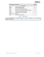
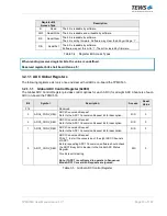
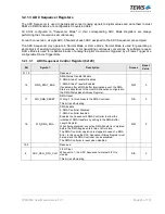
Register Bit
Access Type
Description
R
Read
The bit is readable by software.
R/W
Read/Write
The bit is readable and writeable by software.
R/C
Read/Clear
The bit is readable by software.
The bit is set by firmware. Software may clear the bit by writing a ‘1’.
R/S
Read/Set
The bit is readable by software.
Software may set this bit to ‘1’. The bit is cleared by firmware.
Table 3-4 : Register Bit Access Types
When reading reserved register bits, the value is undefined.
Reserved register bits shall be written as '0'.
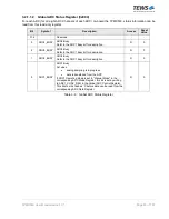
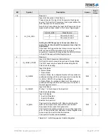
3.2.1.1 ADC Global Registers
The following registers exist only once and deal with all ADCs on-board the TPMC533.
3.2.1.1.1
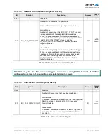
Global ADC Control Register (0x000)
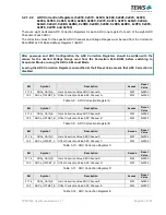
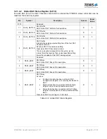
The Global ADC Control Register provides control options for each ADC (for all eight ADC Channels of each
ADC) on-board the TPMC533.
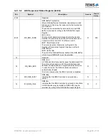
Bit
Symbol
Description
Access
Reset
Value
31:4
-
Reserved
-
-
3
ADC4_CONV_REQ
ADC4 Conversion Request
Refer to the ADC1 Conversion Request bit for description.
R/S
0
2
ADC3_CONV_REQ
ADC3 Conversion Request
Refer to the ADC1 Conversion Request bit for description.
R/S
0
1
ADC2_CONV_REQ
ADC2 Conversion Request
Refer to the ADC1 Conversion Request bit for description.
R/S
0
0
ADC1_CONV_REQ
ADC1 Conversion Request
Write ‘1’ to start the conversion of the eight ADC Channels
of ADC1.
Before requesting ADC1 Conversion, software should check
the ADC1 Busy Bit to be clear in the Global ADC Status
Register.
This bit is self-clearing.
Note: If ADC1 is configured to operate in Sequencer
Mode ADC1 Conversion Requests are ignored.
R/S
0
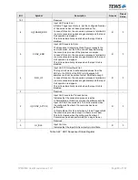
Table 3-5 : Global ADC Control Register

