Circuit descriptions and abbreviation list
GB 84
EM1A
9.
voltage polarity at the secondary winding is negative
(due to different winding direction), meaning that diode D
will block. Capacitor C will discharge via RL, UOUT will
decrease.
•
Opening switch 'S' will generate a counter-e.m.f. in the
primary winding, trying to maintain current ID. Through
this the polarity of the secondary voltage will inverse. The
magnetic energy, stored in the coil, will now be
transformed to the secondary side. Diode D will now
conduct, capacitor C will be charged and UOUT will
increase.
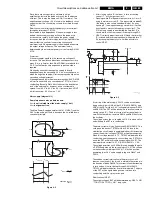
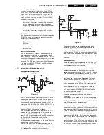
Figure 9-4
To apply this on the EM1A (diagram A2): replace Switch 'S'
by FET TS7102, coil L by L5101, diode D by D6107//D6111
and C by C2104.
Time interval t0 - t1:
After switching on the set, the gate of MOSFET TS7102 will
be high (max. 15 V due to zenerdiode D6105). This will drive
the FET into saturation (UDS = 0 V). The DC-voltage
UMAINS will be transposed across the primary winding of
L5101 (3, 5) resulting in a linear increasing current through
this coil.
The voltage across the co-coupled coil (1, 2) is also positive
and will keep the FET into conductivity via C2101, R3103,
R3105, R3102 and R3117 for some time. The slope of the
primary current is determined by the self-induction of the coil
and on the magnitude of the supply voltage (+375 V).
The maximum current is determined by the time the FET
stays into conductance (t0 - t1). This time is directly
determined by the voltage across R3108//R3118. This
voltage is a measure of the current and if it exceeds 1.4 V,
TS7101 will be driven into conductivity and consequently
connect the gate of TS7102 to earth; the FET will block. The
current will be: 1.4 V/(10//4.7 ohm) = 0.43 A.
The voltage across the secondary winding (8, 9) will be
negative, diodes D6111 and D6107 will block.
Time interval t1 - t2:
The sudden current interruption in the primary coil, will
induce a counter-e.m.f. that wants to maintain the current.
The voltage on the drain of the FET will increase. The
secondary voltage (8, 9) will become positive and will charge
C2104 via D6107 and D6111. All energy that was stored in
L5101 during t0 - t1 will be transferred into the load. Due to
the transformer principle, a voltage will now be induced in the
primary winding (3, 5) and the co-coupled winding (1, 2). This
voltage will be: N * USEC (N = winding ratio).
The voltage across the co-coupled coil will be negative,
keeping the FET blocked.
Time t2:
At t2, the current through the secondary coil will be reduced
to zero, as C2104 is no longer charged. As a consequence,
the voltages will decay and will change polarity. The gate of
the FET will be again made positive, is driven into
conductivity and the cycle starts again.
Feedback, stabilisation:
The Standby Power Supply always oscillates at maximum
power; the only limiting factor is the maximum primary
current that has been pre-set with R3108//3118.
UOUT is determined by R3114, R3124 and zenerdiode
D6122. If the voltage across R3114 exceeds the threshold
voltage of the diode of the optocoupler 7104 (
±
1 V) or, in
other words, UOUT exceeds 5.2 V the transistor of the
optocoupler will conduct.
Transistor TS7100 will be driven and a negative voltage will
be transposed to the emitter of TS7101. When TS7101
conducts, the gate of the FET is at earth potential forcing the
oscillator stop. Due to the load, the secondary voltage UOUT
will decrease. At a certain voltage, optocoupler TS7103/04
will block and the oscillator will start again.
CL 96532156_021.eps
250100
3103
1K
3113
15R
3124
6122
68R
3V9
RL
7101
6105
15V
3102
1K
3117
47R
3126
10K
3125
15R
7100
3104
47R
3101
6M8
3127
5K6
3120
10R
3106
2K2
3107
2K2
2101
2n2
5102
-20V
6107
6103
U
MAINS
U
OUT
2104
2
µ
2
D
S
G
6106
20V
3114
220R
6108
3108
//3118
+5V2
8
9
HOT
COLD
2109
330N
6111
GND-STB
GND-STB
2
1
3
5
2114
7102
10n
2102
10
µ
+
U
A
U
A
U
D
U
D
U
MAIN
I
SEC
I
PRIM
I
PRIM
I
SEC
7103/04
t
t
t
t
N.Usec
ON
OFF
t
0
t
1
t
2
5101
3110
10R
+375V

