Circuit descriptions and abbreviation list
GB 89
EM1A
9.
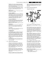
During the 1st frame, 3 pulses are generated to adjust the
cut-off voltage at a current of 8
µ
A. With this measurement
the black level at the RGB-outputs is adjusted. So at start-up
there is no monitor pulse anymore.
At start-up, the HOP measures the pulses, which come back
via pin 44. The RGB-outputs have to be between 1.5 V and
3.5 V. If one of the outputs is higher than 3.5 V or one of them
lower then 1.5 V, the RGB-outputs will be blanked.
Geometry control
All geometry control is done via I2C and the data is stored in
the NVM (IC7012) of the SSB.
Line drive (LINEDRIVE1).
Line drive is derived from an internal VCO. As a reference an
external resonator is used (1301). The internal VCO is locked
with the HD100-pulse, which comes from the PICNIC. The
'PHI-2' part in the HOP receives the HFB_X-RAY_PROT (pin
13) to correct the phase of the line drive. The EHT-info is
supplied to pin 14 (DYN-PHASE-CORR) to compensate
picture breathing depending on the beam current.
Frame drive (FRA).
The VD100 signal from the PICNIC will be extended for 16.5
lines by the circuit around TS7309 and 7311. The resulting
signal (VDHOP) will drive TS7310. This will result in the
(asymmetric) FRA signal.
Note: The Frame outputs (pins 1/2) of the HOP are not used!
East/West drive.
At pin 3 the E/W-drive is available. Pin 4 is a feedback input
for the EHT-info and is used to prevent pumping of the
picture. EHT varies also dependent of the beam current.
Frame rotation.
For frame rotation a control voltage is used from pin 25 of the
HOP. This voltage can vary from 0.4 till 4 V.
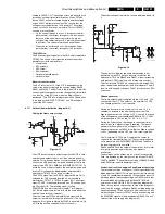
Guarding protections:
•
Flash detection:
When a flash occurs, the EHT-info will become negative very
fast. Via D6303/D6304/R3316, TS7303 starts to conduct.
This makes pin 5 of HOP high. When pin 5 of HOP is high,
then the output (pin 8) is immediately stopped. If the H-drive
stops, then also pin 5 will be low again, which will reset the
flash detection. A bit (FLS) will be set in an output status
register, so via the Painter it can be seen when there was a
flash. This FLS-bit will be reset when the Painter has read
that register.
•
HFB protection:
If the HFB is not present then this will be detected via the
HOP. The Painter puts the TV into protection and an error
code will be generated.
9.1.9
Synchronisation (diagram B3 & B4)
The HIP video processor provides vertical and horizontal
sync pulses V
A
and H
A
, which are synchronised with the
incoming CVBS signal. These pulses are fed to the PICNIC
where they are doubled to be synchronous with the 100 Hz
picture. The outgoing pulses, V
D100
and H
D100
are fed to the
HOP that supplies the vertical and horizontal drive pulses
and the 2f
H
sandcastle pulse.
The VD100 pulse from the PICNIC is only one line long.
Therefore this pulse is converted into a VDHOP signal by a
530
µ
s monostable oscillator (extended by 16.5 lines). This
signal is on block function level equal to VSYNC and
FRA.
The Painter is synchronised on the HD100 pulse from the
FBX and on the VSYNC for the synchronisation of TXT/OSD.
When no CVBS is offered to the video processor, the VA and
HA pulses are switched off by the HIP, and the VD and HD
pulses are then generated by the PICNIC. This to assure a
stable OSD.
9.1.10 Horizontal (line) deflection (diagram A3)
Driving the line output stage
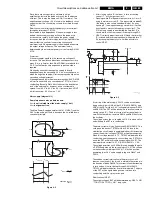
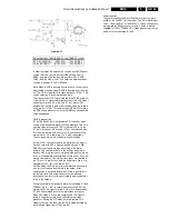
Figure 9-8
The HOP (located on the SSB) generates the line-drive
pulses (LINEDRIVE1), which have a frequency of 31250 Hz
(T = 32
µ
s).
When the LINEDRIVE1 signal is high, TS7409 and TS7408
will conduct. A constant DC voltage will be applied across
L5410, causing a linear increasing current through this coil.
The secondary voltage of L5410 has a negative polarity so
that TS7421 will block. When switching on the set, the
current through L5410 is supplied by the 5V2 Standby supply
(via D6407), and taken over by the +11D voltage (via D6408)
of the main supply.
When the LINEDRIVE1 signal becomes low, TS7409 and
TS7408 will block. The voltage polarity across the primary
winding of L5410 will invert. The positive voltage on the
secondary winding will now drive TS7421 into conductivity.
Because of the storage time of the line transistor (TS7421),
L5410 cannot transfer its energy immediately to the
secondary side. This may result in high voltage peaks on the
collector of TS7409 and TS7408. To prevent that these
peaks will damage the transistors, a 'snubber' circuit (C2414,
C2412 and R3411) will suppress them.
When the LINEDRIVE1 signal is high again, the above-
described sequence starts again. Circuit L5411 and R3409
will increase the switch-off time of the line transistor.
The line stage will be started via the 'slow start' principle.
During start-up, the HOP generates line drive pulses with a
small TON and a high frequency (50 kHz); TOFF will be
constant and TON will be gradually increased until the duty-
cycle is 50 % (normal condition). The time interval from start
to normal condition takes about 150 ms. When switching off,
the same procedure is followed, but now in reverse order.
Operation of the line output stage
To explain the operation of the line output stage, we use the
following start conditions:
•
C2433 is charged to max. 141 V (VBAT)
•
TS7421 is driven into conductivity.
CL 96532156_013.eps
260100
3481
6480
2426
6422
2421
7480
3414
2415
3406
3485
3431
5421
2431
6481
2480
3483
141V
141V
7482
3418
HOT
COLD
2425
6423
2432//33//34
6408
6407
3409
5411
2414
5410
3411
2412
7408
+8V
7409
MAIN 11D
STANDBY 5V2
2402
T
ON
T
OFF
3407
3487
2420
7421
5430
2417
3417
3486
3484
7481
3404
LINEDRIVE 1
(HOP)
EW_DRIVE
(HOP)
ST
AR
T
NORMAL
T7421 conducting
1
2
5
1
2
1
4
3
LINE DEFL. COIL.
LINEARITY
COIL.
5422
Caused by
serial losses in
the line output stage
Linearity Correction
S-correction
X
Y
X
Deflection centre
X > Y
(
*
1)
*
2
(
*
2)
*
1


