Circuit descriptions and abbreviation list
GB 86
EM1A
9.
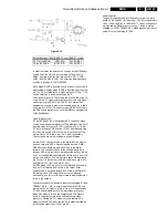
To stabilise the output voltage, a feedback loop is
implemented, which will reduce TON when VBAT increases
and vice versa.
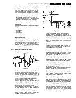
Via a voltage divider, excisting of (1 %) resistors R3507,
R3510 and R3527, a voltage of 2.5 V (when VBAT = 141 V)
is fed to the input of precision shunt regulator 7506. This
regulator will conduct, a current will flow through R3524 and
TS7505 will be driven into conductivity. The base of TS7502
will now be set at a certain positive voltage. As this transistor
switches the FET TS7504 on and off, this circuit can
determine the dutycycle.
E.g. when the load increases, VBAT will decrease. As a
consequence, the input-voltage of regulator 7506 will
decrease, resulting in a lower current. Through that, the
emitter-base voltage of TS7505 will diminish.
The current through R3504 will decline, changing the base-
voltage of TS7502 and through that the TON (will increase)
of the FET. The output voltage VBAT will rise.
If the load continues to increase, the regulator will block at a
certain moment, the collector-current of TS7505 will now be
zero. If there flows no current through R3504, TON will now
be maximum (IMAX = 1.4 A). This is the point where VBAT
will be below 141 V, and at further increasing load will be
switched off (The voltage across the co-coupled coil (4, 5) will
decrease due to the increasing load. Therefore the voltage
on the gate of TS7504 comes below the threshold voltage.
The supply switches off and an audible hiccuping can be
heard).
On the other hand when the load decreases, VBAT will rise.
As a consequence, the input-voltage of 7506 will also rise
resulting in a higher current. The current through R3504 will
rise, changing the base-voltage of TS7502 and through that
the TON (will decrease) of the FET. The output voltage VBAT
will be reduced.
If, for instance, VIN will decrease (e.g. UMAINS is 180 V i.s.o.
240 V), the slope of the drain-current will be flattened,
through which the FET will be longer into conductance,
keeping VOUT constant.
If, for any reason, the stabilisation circuit might fail, the output
voltage VBAT can never exceed 200 V (via D6514). D6514
will form a shortcircuit, VBAT will drop and the set will switch
off (this will result in an audible hick-uping of the supply).
Set to 'STANDBY" (via RC):
When the set is switched to 'STANDBY' via the Remote
Control, the Main supply will be switched off.
This is done by the circuit around TS7529 (see diagram A1):
During 'ON'-state the Main supply is fed with line pulses via
the STANDBY line. They are rectified and smoothed via
D6517, D6516 and C2530 and fed to TS7529. Because they
are less than -20 V, this transistor will be blocked.
When these pulses are stopped (STANDBY), TS7529 will be
saturated and TS7502 will be switched off. This will switch off
the Main supply.
Set to 'ON' (via 'STANDBY'):
At the moment the set is switched 'ON', the HOP is not
working (as much as possible IC's are made voltageless
during 'STANDBY'). Therefore it is impossible that the
STANDBY line carries line-pulses, so the main supply cannot
start up. This problem is solved via the 'low power start-up'
possibility of the HOP.
Via pin 22, the HOP receives, via the STANDBY_INFO line
from the Painter, a voltage of 5.2 V coming from the Standby
supply. The result will be that the HOP will generate pulses
with a nominal TOFF and TON growing from 0 to 30 % of the
nominal value.
This signal is unchanged until the Main supply is switched
'ON' and the HOP the correct I
2
C-command POR-bit) has
received.
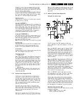
Guarding circuit:
The negative pulses on the secondary winding of L5506 are
rectified by D6520 and smoothed by C2535. The resulting
negative DC-voltage will keep TS7510 blocked, even as
TS7511.
When something happens in the Main supply through which
these pulses will decrease, the DC-voltage will increase.
TS7510 starts to conduct, even as TS7511. Via R3541 and
D6522 this situation will be maintained (thyristor principle).
The collector of TS7511 drives via R3538 a positive pulse
back to the Painter (named STANDBY(POR)). The Painter
will now switch off the Main supply via the STANDBY_INFO
signal.
SSB
There are 3 voltages used for the SSB: +8 V, +5.2 V and +5
V.
+5.2 V is the Standby voltage; it should always be present.
The 8 V is derived from the 11D V with stabiliser 7906 (on
LSP). This 11D voltage is only present when the line-drive
pulses start the deflection.
The 8 V is used to switch the +5.2 V with transistor 7905 to
supply the +5 V.
9.1.4
Control & Teletext (diagram B7)
Painter
The SAA5667 (IC7001) is called the Painter (OSD, TXT and
Control). In this IC, the microprocessor and the TXT-decoder
(level 2.5) are integrated.
Some of its functions are:
•
Set control.
•
TXT/OSD acquisition.
•
RGB-outputs to the HOP
•
Menu blending; for blending the contrast is software
controlled.
•
I/O-ports for I2C, RC5, LED, and service modes.
•
Error code generation.
The software for EM1A can be 192 kB.
For TXT-data 100 pages can be stored in IC7011.
The Non Volatile Memory IC7011 is a 4-kb version M24C32.
All ICs in this part are supplied with 3V3. For this voltage a
3V3 stabiliser is used (IC7005).
When the 3.3 V is available, a POR is generated with
TS7003/7004 to wake up the Painter. During the reset all I/O
pins are high. When a POR is generated the TV-set is in
Standby mode.
The horizontal (HD100) and vertical (VSYNC) sync pulses
are also fed to the Painter for stable OSD and TXT.
Teletext
The TXT-decoder in the Painter gets its video signal directly
on pin 31 (from the HIP).
The RGB-outputs are available on pins 46/47/48. Fast
blanking is realised via pen 52.
A separate memory is used to store the TXT information
(IC7011).
I
2222
C
In the EM1A-chassis with Painter-processor there are two
I
2
C-busses used:
•
Slow (max. 100 kHz) hardware I
2
C-bus (called I
2
C1),
used for all IC communication.
•
Separate short bus (called I
2
C3) for the Non Volatile
Memory (NVM) to avoid data corruption.


