OEM6 Family Installation and Operation User Manual Rev 7
131
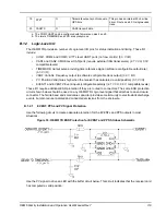
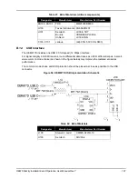
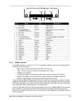
Figure 62: Top-view, P1502 Expansion 16-Pin Header
C.1.2
CMOS Level I/O
The OEM628 provides a number of 2.7 V (3.3 V-compatible) CMOS level I/O pins for status indication
and timing. These I/O include:
•
PPS: Pulse-Per-Second (software configurable to other rates)
•
VARF: Variable Frequency (a software configurable clock output)
•
ERROR: Error indication
•
PV: Position Valid (used to indicate when the receiver has calculated a valid position)
•
EVENT1 and EVENT2: Event inputs (active high by default with configurable polarity)
•
USERIO1 and USERIO2: User GPIO (available through NovAtel’s API)
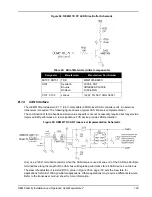
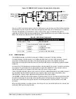
These I/O require additional ESD protection if they are routed to connectors. Some users may require
additional drive strength on the PPS signal. The figure below shows a suitable buffer that may be used.
R103 in the schematic may be used to limit the drive strength of the PPS output if required. This buffer
has a propagation delay of approximately 5 to 6 nanoseconds.
The same ESD protection circuit shown below should be used on any OEM628 CMOS level signal that
will be routed to an enclosure connector. The ferrite bead and small value capacitor provide some
immunity to electrostatic discharge events, but also serve to reduce radiated and conducted emissions
from the enclosure.
Pin
Signal
Type
Description
1
ETH_RD-
Input
Ethernet Rx-
2
Input
Ethernet Rx+
3
3V3 (for Ethernet
magnetics center tap)
Output
Rx centre tap power for Ethernet
magnetics
4
Output
Ethernet Tx+
5
ETH_TD-
Output
Ethernet Tx-
6
3V3 (for Ethernet
magnetics center tap)
Output
Tx center tap power for Ethernet
magnetics
7
LED_A
Output
Activity/Link
8
LED_B
Output
100 BT
9
GND
REF
GND
10
CAN1TX
Output
CAN1TX
11
CAN1RX
Input
CAN1RX
12
CAN2TX
Output
CAN2TX
13
CAN2RX
Input
CAN2RX
14
Reserved
Input
UID
15
VBUS
Input
VBUS
16
GND
REF
GND
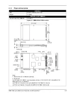
Pin 2
Pin 1
Pin 24
Pin 23
Pin 2
Pin 16
Pin 15
Pin 1


