OEM6 Family Installation and Operation User Manual Rev 7
107
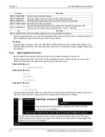
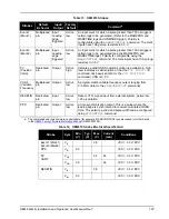
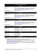
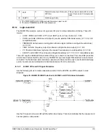
Table 13: OEM615 Strobes
Table 14: OEM615 Strobe Electrical Specification
Strobes
Default
Behavior
Input/
Output
Factory
Default
Comment
a
Event1
(Mark 1)
Multiplexed
pin
Input
Leading
edge
triggered
Active
low
An input mark for which a pulse greater than 150 ns triggers
certain logs to be generated. (Refer to the MARKPOS and
MARKTIME logs and ONMARK trigger.) Polarity is
configurable using the
MARKCONTROL
command. The mark
inputs have 10K pull-up resistors to 3.3 V
Event2
(Mark 2)
Multiplexed
pin
Input
Leading
edge
triggered
Active
low
An input mark for which a pulse greater than 150 ns triggers
certain logs to be generated (see the MARK2POS and
MARK2TIME logs). Polarity is configurable using the
MARKCONTROL
command. The mark inputs have 10K pull-up
resistors to 3.3 V
PV
(Position
Valid)
Dedicated
pin
Output
Active
high
Indicates a valid GNSS position solution is available. A high
level indicates a valid solution or that the
FIX POSITION
command has been set (refer to the
FIX POSITION
command). VDD is 3.3 V
VARF
(Variable
Frequency
)
Multiplexed
pin
Output
Active
low
A programmable variable frequency output ranging from
0 -5 MHz (refer to the
FREQUENCYOUT
command)
RESETIN
Dedicated
pin
Input
Active
low
Reset LVTTL signal input from external system; active low,
>
20 µs duration
PPS
Dedicated
pin
Output
Active
low
A time synchronization output. This is a pulse where the
leading edge is synchronized to receiver-calculated GNSS
Time. The polarity, period and pulse width can be configured
using
PPSCONTROL
command
a. The commands and logs shown in capital letters (for example, MARKCONTROL) are discussed in further detail
in the
OEM6 Family Firmware Reference Manual
(OM-20000129).
Strobe
Sym
Min
(V)
Typ
(V)
Max
(V)
Current
(mA)
Conditions
Event1 (Mark 1)
Event2 (Mark2)
PPS
V
IL
0.8
VCC = 3.3 V; 85
C
V
IH
2.0
VCC = 3.3 V; 85
C
PV
VARF
V
OL
0.4
24
VCC = 3.3 V; 85
C
V
OH
3.0
24
VCC = 3.3 V; 85
C
RESETIN
V
IL
0.8
VCC = 3.3 V; 85
C
V
IH
2.3
VCC = 3.3 V; 85
C


