OEM6 Family Installation and Operation User Manual Rev 7
157
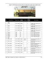
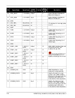
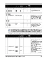
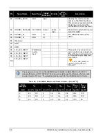
Figure 79: J4101 Expansion Header Pinout and Signal Description (odd numbered pins)
Pin
Signal Name
Signal Type
Signal
Direction Polarity
Drive
Strength
(mA)
Description
1
GND
-
-
3
TXD4
3.3V CMOS Output
-
2
COM4 UART Signaling (3.3 V
CMOS logic)
5
RXD4
3.3V CMOS Input
-
-
COM4 UART Signaling (3.3 V
CMOS logic)
7
RTS4
3.3V CMOS Output
-
2
COM4 UART Signaling (3.3 V
CMOS logic)
9
CTS4
3.3V CMOS Input
-
-
COM4 UART Signaling (3.3 V
CMOS logic)
11
CAN1+
CAN
IO
-
-
CAN1+ Differential Signal
13
CAN1-
CAN
IO
-
-
CAN1- Differential Signal
15
CAN2+
CAN
IO
-
-
CAN2+ Differential Signal
17
CAN2-
CAN
IO
-
-
CAN2- Differential Signal
19
GND
-
-
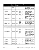
21
SPI1_nCS0
3.3V CMOS Output
Active
Low
2
Serial Peripheral Interface #1,
Chip Select 0.
23
SPI1_SCLK
3.3V CMOS Output
-
2
Serial Peripheral Interface #1,
Serial Clock.
25
SPI1_MOSI
3.3V CMOS Output
-
2
Serial Peripheral Interface #1,
Master Out / Slave In
27
SPI1_MISO
3.3V CMOS Input
-
-
Serial Peripheral Interface #1,
Master In / Slave Out
29
SPI1_nCS1
3.3V CMOS Output
Active
Low
2
Serial Peripheral Interface #1,
Chip Select 1.
31
SPI4_nCS0
3.3V CMOS Output
Active
Low
2
Serial Peripheral Interface #4,
Chip Select 0.
33
SPI4_SCLK
3.3V CMOS Output
-
2
Serial Peripheral Interface #4,
Serial Clock.


