OEM6 Family Installation and Operation User Manual Rev 7
118
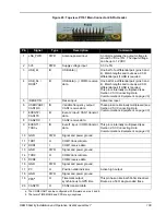
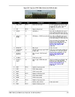
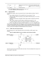
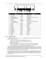
Figure 52: Top-view, P1101 Main Connector 20-Pin Header
Pin
Signal
Type
Description
Comments
1
LNA_PWR
PWR
Antenna power input
An LDO regulates the output voltage
to around 5 VDC ±10%. The input
voltage can be up to 12 VDC
2
3V3
PWR
Supply voltage input
3.3 V ±5%
3
USB_D-
IO
USB data (-)
One-half of a differential pair (pins 3
and 4). Match lengths and route as a
90
Ω
differential pair if USB is required
4
USB_D+ /
RXD3
a
IO
USB data (+) / COM3 receive data One-half of a differential pair (pins 3
and 4). Match lengths and route as a
90
Ω
differential pair if USB is required
This pin is internally multiplexed. See
Section 2.5.3 Connecting Data
Communications Equipment in the
(OM-
20000128).
5
RESETIN
I
Reset input
Active low reset
6
USERVARF /
CAN1RX
IO
Variable frequency output / CAN1
receive data
These pins are internally multiplexed.
See Section 2.5.3 Connecting Data
Communications Equipment in the
(OM-
20000128).
7
EVENT2 /
CAN1TX
IO
Event 2 Input / CAN1 transmit
data
8
CAN2RX
I
CAN2 receive data
9
EVENT1 /
TXD3
a
IO
Event1 input / COM3 transmit
data
This pin is internally multiplexed. See
Section 2.5.3 Connecting Data
Communications Equipment in the
(OM-
20000128).
10
GND
PWR
Signal and power ground
11
TXD1
O
COM1 transmit data
12
RXD1
I
COM1 receive data
13
GND
PWR
Signal and power ground
14
TXD2
O
COM2 transmit data
15
RXD2
I
COM2 receive data
16
GND
PWR
Signal and power ground
17
PV
O
Position valid indicator
Active high output
18
GND
PWR
Signal and power ground

