


OEM6 Family Installation and Operation User Manual Rev 7
153
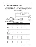
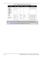
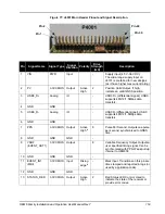
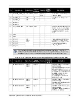
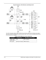
Figure 77: J4001 Main Header Pinout and Signal Description
Pin 2
Pin 1
Pin 40
Pin 39
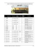
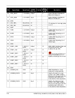
Pin
Signal Name
Signal Type
Signal
Direction Polarity
Drive
Strength
(mA)
Description
1
VIN
PWR
Input
-
Supply Input (4.5 V-36 VDC).
The wide-range supply input on
J4101 is preferred for new designs
(as it has a higher max current rating).
2
PV
3.3V CMOS Output
Active
High
2
Position Valid Output. If high,
indicates a valid GNSS position.
3
Analog
IO
-
USB0 D+ (differential signal). USB0
supports 480/12/1.5Mbps data
transfers.
4
GND
GND
-
5
USB0_D-
Analog
IO
-
USB0 D-(differential signal). USB0
supports 480/12/1.5Mbps data
transfers.
6
GND
GND
-
7
PPS
3.3V CMOS Output
Active
High
b
8
Pulse Per Second. Outputs one pulse
per second, synchronized to GNSS
time.
8
GND
GND
GND
-
9
VARF
(EVENT_OUT1)
3.3V CMOS Output
8
Variable Frequency Output. Outputs a
user specified timing signal. Can be
synchronized with PPS. Weak pull up
internal to OEM638
10
GND
GND
GND
-
11
EVENT_IN1
(MKI)
3.3V CMOS Input
Rising
edge
b
-
Mark Input. Transitions on this pin are
time stamped and reported in logs (or
used by application code).
12
GND
GND
GND
-
13
STATUS_RED
3.3V CMOS Output
Active
High
2
Red Status LED Control. Used to
indicate the state of the receiver or
provide error codes.