OEM6 Family Installation and Operation User Manual Rev 7
163
E.1.2
Power Supply
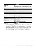
The OEM638 receiver can operate from either:
•
3.3 V +5%/-3% at up to 2.0 A
or
•
4.5 V to 36 VDC input supply at up to 1.5 A
Power consumption will vary greatly, depending on which features are active.
The OEM638 has integrated reverse voltage protection (to -10 VDC) on its 3.3 V supply input port. The
Wide-Range supply port is reverse protected to -40 VDC.
If operating from the 3.3 V supply input, bulk supply bypassing (approximately 50 uF) and high frequency
bypassing (0.1 uF and 220 pF) near the 3.3 V supply pin is recommended for optimal performance. If
operating from the Wide-Range supply, high-frequency bypassing (0.1 uF and 220 pF) is recommended.
E.1.3
Antenna Power Output
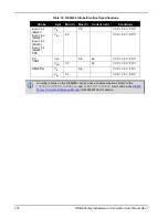
The OEM638 card supplies a software-selectable 3.3 V or 5 V to the center pin of the MMCX RF
connector to power an external antenna (the return is the outer conductor of the coax). There is also the
option to provide an external voltage to the LNA (up to 18 VDC).
This port is capable of providing up to 200 mA to a connected antenna. The typical current draw for a
NovAtel antenna is 25-40 mA.
The internally-generated 3.3 V and 5 V supplies are over current protected. If the external LNA supply is
used, the supply
must
self-limit to 125 mA max to avoid damage to the OEM638 receiver. (There is no
over current protection on the external LNA supply input.)
E.1.4
Logic-Level I/O
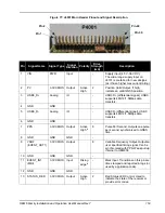
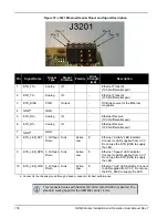
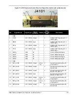
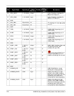
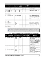
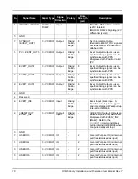
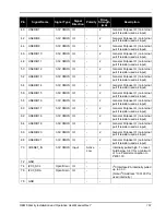
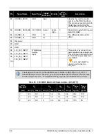
The OEM638 provides a number of 3.3 V Logic-level I/O pins for status indication, communication and
timing:
•
PPS:
Pulse-Per-Second
•
VARF:
Variable Frequency (a software-configurable clock output)
•
ERROR:
Error indication
•
PV:
Position Valid (Used to indicate when the receiver has calculated a valid position)
•
STATUS_RED / STATUS_GRN:
Receiver status indicators (used to control external LEDs)
•
COM3 / COM4 / COM5:
UARTs (including RTS/CTS flow control)
•
EVENT_IN(1,2,3,4):
Event Inputs
•
EVENT_OUT(1-6) + SYNCOUT (EVENT_OUT7):
Event Outputs
•
USERIO(0-21) 2xI2C, 2xSPI:
User GPIO and additional interfaces (available through NovAtel’s
UserApp API)
These I/O require additional ESD protection if they are to be routed to connectors.
Some users may require additional drive strength on the PPS signal. The
a suitable buffer that may be used. R222 may be used to limit the drive strength of the PPS output buffer
(if desired). This buffer has a propagation delay of approximately 5-6 nanoseconds.
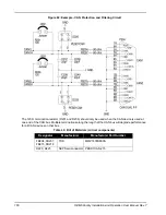
A similar ESD protection circuit to the one shown below should be used on any OEM638 Logic-level
signal that will be routed to an enclosure connector. (If an EVENT_IN or EVENT_OUT line is routed to an
enclosure connector the capacitance must be minimized—these signals may require buffering in some
applications.)


