background image

Chapter 4

Chapter 6

Memory and I/O Usage

Appendix A

Appendix C

Pr
eface

Chapter 4Chapter 5

LS PRO HARDWARE TECHNICAL REFERENCE  5/15

Ethernet controller

The Ethernet controller on the LS Pro system board uses a block of 17 I/O ports from

0300h to 0310h.

Port

Function

300

82596 PORT address

0301-0303

reserved

304

82596 CA address

0305-0307

reserved

0308-030F

Ethernet ID PROM

310

Ethernet status register

82596 PORT

This is a 16-bit write only port. The data definition of this port is given in the

address

manufacturers data book.

82596 CA

This is a 16-bit write only port that has no data associated with it. An access to this

address

port activates the CA control signal. A definition of the operation of this port is

given in the manufacturers data book.

Ethernet ID

The lower six bytes of the ID PROM contain the six byte Ethernet ID.

PROM

Port

ID byte

308

0

309

1

030A

2

030B

3

030C

4

030D

5

030Eh is reserved, and 030Fh contains a checksum for the other seven bytes.

Ethernet status

This port has different functions in read and write cycles.

register

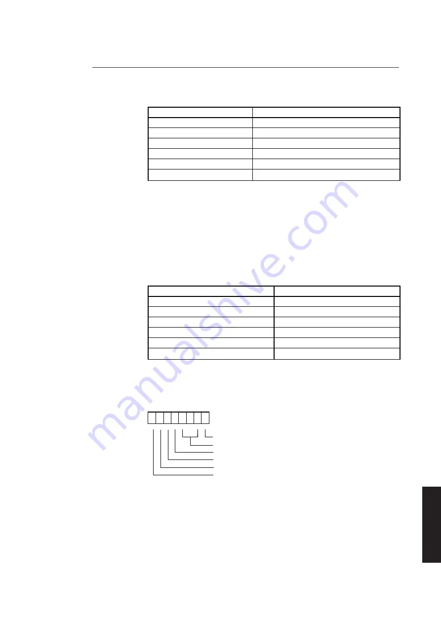
7      6      5      4     3     2     1      0

596IRQ

reserved

LAN ID0

LAN ID1

revision

speed

Bit 0

This bit returns the current state of the IRQ line from the 82596

Ethernet coprocessor.

Bits 1-3

Reserved.

Summary of Contents for Apricot LS Pro

Page 1: ...apricot HARDWARE TECHNICAL REFERENCE MITSUBISHI ELECTRIC LS Pro ...

Page 2: ...HARDWARE TECHNICAL REFERENCE ...

Page 3: ...itment on the part of Apricot Computers Limited The software described in this manual is furnished under a license agreement The software may be used or copied only in accordance with the terms of this agreement It is against the law to copy any disk supplied for any purpose other than the purchaser s personal use All rights reserved no use or disclosure without written consent Copyright Apricot C...

Page 4: ...e rear of the system unit 3 System Board This section provides an overview of the function of the system board and more detailed descriptions of the processor and interface circuitry Sub sections provide a description of each area of the board 4 Peripheral This section describes each of the system components which attach to either the Items system board e g floppy disk drive or system unit e g key...

Page 5: ...hnical Reference Manual The following manufacturers data sheets give information on specific devices Intel 80386SX 80387SX 8042 Keyboard controller 82077 Floppy disk controller 8237 DMA controller 8254 System timers 8259 Interrupt controllers 82596 Ethernet coprocessor VLSI VL82C311 SCAMP AT chipset Cyrix 486SLC Cirrus CL GD542X video controller National Semiconductor NS16450 Serial communications...

Page 6: ...CONTENTS ...

Page 7: ...4 General 3 14 3 6 Floppy disk controller 3 15 General 3 15 Drive formats 3 15 3 7 Hard disk interface 3 16 General 3 16 Interface signal descriptions 3 16 3 8 Peripherals controller 3 17 Serial ports 3 17 Parallel port 3 18 3 9 Keyboard mouse controller 3 18 General 3 18 Keyboard password security 3 18 3 10 LOC Technology 3 19 3 11 Ethernet port 3 19 General 3 19 3 12 Apricot Business Audio 3 21 ...

Page 8: ...e 5 2 5 3 I O space 5 4 DMA I O address map 5 5 Interrupt controllers 5 6 System timers 5 6 Keyboard controller 5 6 Port B 5 8 RTC RAM NMI mask 5 9 SCAMP registers 5 10 Apricot ports 5 11 Hard disk drive controller registers 5 14 Serial port controller registers 5 14 Ethernet controller 5 15 Business audio 5 17 Floppy disk controller 5 17 Parallel port controller 5 18 Video DAC 5 19 VGA registers ...

Page 9: ...Chapter 1 INTRODUCTION ...

Page 10: ...apter 6 Contents Chapter 3 Chapter 5 Introduction Chapter 3 Chapter 1 LS PRO HARDWARE TECHNICAL REFERENCE 1 1 Contents 1 INTRODUCTION General 1 2 Variants 1 2 System unit 1 3 Keyboard 1 3 Monitors 1 3 Expansion 1 4 ...

Page 11: ...IBM compatible parallel port Ethernet port Token Ring port optional PS 2 compatible mouse port Floppy disk controller on system board Hard disk connector on system board Full IBM functional compatibility On board VGA On board high resolution video Internal power supply LOC Technology security sub system Socket for 80387SX Windows 3 1 compatible Business Audio subsystem Variants The basic system un...

Page 12: ...ts of the system and identifies functions implemented on the system board Keyboard The keyboard is a full QWERTY typewriter keyboard and numeric keypad together with editing keys The layout of the 102 key UK keyboard is compatible with the IBM AT enhanced keyboard The keyboard is fitted with a PS 2 style miniature DIN connector and any fully compatible keyboard can be plugged into the system unit ...

Page 13: ...sor is fitted on the system board MONITOR POWER SUPPLY FLOPPY DISK DRIVE HARD DISK DRIVE SYSTEM BOARD including PROCESSOR MEMORY VIDEO ADAPTER ETHERNET CONTROLLER SERIAL PORT PARALLEL PORT LOC TECHNOLOGY SECURITY FLOPPY DISK CONTROLLER HARD DISK CONNECTOR KEYBOARD AND MOUSE PORTS BUSINESS AUDIO MOUSE KEYBOARD FAN AC INLET AC OUTLET PARALLEL PORT NETWORK PORTS VIDEO PORT SERIAL PORTS MOUSE PORT KEY...

Page 14: ...Chapter 2 SYSTEM UNIT ...

Page 15: ...work 2 6 Removing the floppy drive 2 7 Removing the power supply metalwork 2 8 Removing the hard disk drive 2 9 Removing the fan 2 10 Removing the power supply 2 11 Removing a Token Ring module 2 11 Removing a parallel port cable 2 13 Removing a thick wire Ethernet assembly 2 13 Removing the system board 2 13 Removing an escutcheon plate 2 14 Removing the power switch linkage 2 14 RFI screening tr...

Page 16: ...R detector for the security card The right side panel contains the keyboard and mouse ports and the audio input and output sockets POWER SWITCH INFRARED SENSOR FLOPPY DISK DRIVE POWER INDICATOR LAN INDICATOR FLOPPY DISK INDICATOR HARD DISK INDICATOR MOUSE KEYBOARD AUDIO IN AUDIO OUT The floppy drive bezel is on the right side of the system unit The rear panel contains the following connectors main...

Page 17: ...o install add ons Dismantling and re assembly The LS Pro range has been designed to meet international EMI and safety standards Warnings and To ensure safety and continued compliance with these standards observe the cautions following precautions It is recommended that modifications are carried out by an authorized dealer Unqualified users should not normally dismantle the equipment Replacementpar...

Page 18: ...th point an earthed bench or bench mat an earthed wrist strap Equipment The following tools are required to dismantle the system unit required Philips screwdriver Flat bladed screwdriver Nut spanner set thin nosed pliers System board Many of the dismantling reassembly procedures which follow involve the connectors disconnection and reconnection of system board plugs and sockets The following table...

Page 19: ... ASSEMBLY SW 1 BATTERY POWER JUMPER HARD DISK SIGNAL FLOPPY DISK HARD DISK POWER LOUDSPEAKER Removing the A keylock on the rear panel of the system unit locks the top cover in place The system unit cover cannot be removed unless this is unlocked The cover is located by a ledge at top cover the front and lugs on the sides and at the rear Two thumbscrews in the rear panel secure the cover ...

Page 20: ... millimetres and lift it clear 5 Replacing the top cover is simply the reverse of removal Check that the keylock is in the unlocked position Make sure that the top cover is properly aligned during replacement and do not force it into position Note It is not necessary to remove cables other than the mains power cable to remove the system unit top cover However in order to remove some of the interna...

Page 21: ...ot to strain the cable or its connectors 6 Lift the system board metalwork clear of the computer 7 Invert the system board metalwork and rest it on a flat surface 8 Replacement is simply the reverse of removal Take care to ensure that the metalwork engages correctly Do not use undue force Route the loudspeaker cable between the front of the system unit and the LEDs Removing the The floppy drive is...

Page 22: ...e top of the system unit fan The system metalwork board metalwork uses the power supply metalwork for location The power supply metalwork is secured by two screws and a number of lugs SECURING LUGS SECURING SCREW SECURING LUGS EARTH BOND SCREW FAN LOCATION SLOT 1 Remove the system board metalwork 2 Remove the earth bond screw which secures the system board escutcheon plate to the power supply meta...

Page 23: ...m right of the metalwork are properly engaged and that the metalwork does not foul on the fan The fan rests on a flexible foam pad which is compressed when the power supply metalwork is in place A slot is provided in the metalwork to allow a small blunt instrument flat bladed screwdriver to push the fan down during the replacement of the metalwork Do not force the power supply metalwork into posit...

Page 24: ...placement ensure that the drive select jumpers are in the same positions as those on the old drive Warning 1 Reconnect the power and signal cables to the drive before putting the drive in position 2 Ensure that the screws which you use to secure the drive are the ones which you removed If you use longer screws you will damage the drive Removing the fan The cooling fan rests on a flexible foam pad ...

Page 25: ...fan 4 Remove the four screws securing the power supply 5 Lift the power supply clear of the system unit 6 Replacement is simply the reverse of removal Ensure that the voltage range selection jumper is in the correct position for the mains supply available The jumper is identified in section 4 of this manual Removing a The Token Ring module is secured to three standoff pillars inside the system uni...

Page 26: ...e Token Ring module the pin assemblies will probably come out with the Token Ring module although they may remain in the system board When the Token Ring module is in position the plate that surrounds the Token Ring connector is between the system unit base and the escutcheon plate The two standoff pillars by the connector nearest the power supply protrude through corresponding holes in the Token ...

Page 27: ...e Ethernet assembly to the escutcheon plate unplug the assembly cable from the system board and lift the assembly clear of the system unit 3 Replacement is simply the reverse of removal Removing the The system board is secured to the base of the system unit by seven screws through system board the system board and four screwlocks through the escutcheon plate The following illustration identifies t...

Page 28: ... 2 Remove the system board 3 Remove the screw that secures the escutcheon plate to the power supply metalwork 4 Remove the three screws that secure the escutcheon plate to the system unit and lift the escutcheon plate clear 5 Replacement is simply the reverse of removal Removing the The power switch linkage mechanically links the system ON OFF switch on the front power switch of the system unit to...

Page 29: ...ystem unit Note There should be no resistance to this movement If there is resistance you have not pushed the linkage far enough back 6 Slide the linkage back through the slot and lift it clear 7 Replacementissimplythereverseofremovalexceptthatgentleinwardpressure must be exerted to the front of the linkage to allow it to pass the front rib Do not force the linkage into place RFI screening tray Th...

Page 30: ...nstalling add ons Memory During manufacture 2 or 4 Mbytes of RAM can be soldered to the system board upgrades System board memory can be expanded to a maximum capacity of 16 Mbytes by fitting SIMMs in sockets provided on the system board When 4 Mbytes of RAM is installed during manufacture four SIMM sockets are fitted When 2 Mbytes of RAM is installed six SIMM sockets are fitted SIMMs must be inst...

Page 31: ... Removing SIMMs If you wish to install an upgrade in a pair of SIMM sockets which are already occupied you must first remove the existing SIMMs Starting with the SIMM nearest the rear of the system unit and working towards the front 1 Lever the metal clips on each side of the socket gently away from the SIMM using your thumbnails When the clips are far enough apart the top edge of the SIMM will mo...

Page 32: ...or strip nearest the system board 2 Position the SIMM above the socket at an angle of about 15 3 Lower the SIMM towards the socket The right edge of the SIMM will be prevented from reaching the connector by the securing clip 4 Allow the left edge of the SIMM to drop into the connector 5 Push the SIMM gently to the right and lower the right edge into the connector 6 Ensure that the SIMM is properly...

Page 33: ...etalwork 3 Locate the 80387SX socket from the following illustration PIN 1 80387SX SOCKET 4 The 80387SX has a positioning guide in the form of a circular recess Insert the 80387SX in the socket with the positioning guide at pin 1 making sure that you do not bend or otherwise damage the pins Note The 80387SX only fits in one orientation Do not use excessive force or damage may occur 5 Reassemble th...

Page 34: ...NA Green rtn Mono rtn Green rtn 8 NA Blue rtn No pin Blue rtn 9 NA Plug No pin No pin 10 NA Digital Gnd Digital Gnd Digital Gnd 11 NA Reserved No pin Digital Gnd 12 NA Reserved Digital Gnd No pin 13 O Hsync Hsync Hsync 14 O Vsync Vsync Vsync 15 NA Reserved No pin No pin Ethernet Thick The thick Ethernet connector is a 15 pin female D shell 1 8 9 15 which uses a slide to hold the male and female co...

Page 35: ...ta 7 Not used 8 Not used Serial The serial port uses a male 25 pin D shell 1 13 14 25 connector Pin I O Signal name 2 O Transmit data COM1 3 I Receive data COM1 4 O Request to send COM1 5 I Clear to send COM1 6 I Data set ready COM1 7 NA Signal ground 8 I Data carrier detect COM1 12 I Data carrier detect COM2 13 I Clear to send COM2 14 O Transmit data COM2 16 I Receive data COM2 19 O Request to se...

Page 36: ...15 I Error 3 I O Data bit 1 16 O Init 4 I O Data bit 2 17 O Slct In 5 I O Data bit 3 18 NA Ground 6 I O Data bit 4 19 NA Ground 7 I O Data bit 5 20 NA Ground 8 I O Data bit 6 21 NA Ground 9 I O Data bit 7 22 NA Ground 10 I Ack 23 NA Ground 11 I Busy 24 NA Ground 12 I PE 25 NA Ground 13 I SLCT Keyboard mouse The keyboard and mouse connectors are miniature 6 pin 6 4 2 1 3 5 connectors DIN connectors...

Page 37: ...Chapter 3 SYSTEM BOARD ...

Page 38: ...System memory 3 10 General 3 10 Read only memory ROM 3 10 Random access memory RAM 3 10 Real time clock RTC RAM 3 11 Contents of RTC RAM 3 11 3 5 Video adapter 3 14 General 3 14 Video controllers 3 15 3 6 Floppy disk controller 3 15 General 3 15 Drive formats 3 15 3 7 Hard disk interface 3 16 General 3 16 Interface signal descriptions 3 16 3 8 Peripherals controller 3 17 Serial ports 3 17 Programm...

Page 39: ...Under certain circumstances the system may display a prompt asking for the SIN to be entered If this happens refer to the Owner s Handbook and associated documentation If Apricot s LOC Technology software is in use refer to the documentation supplied with the software Major The following list of major components on the system board identifies the custom chips components and briefly details their f...

Page 40: ... in the following illustration TOKEN RING MODULE CONNECTOR PARALLEL PORT SOCKET PERIPHERALS CONTROLLER KEYBOARD CONTROLLER TOKEN RING MODULE CONNECTOR THICK ETHERNET SOCKET POWER CONNECTOR SIMM SOCKETS R A M 80387SX SOCKET ETHERNET CONTROLLER SCAMP AUDIO PROCESSOR FLOPPY CONTROLLER HARD DISK DRIVE CONNECTOR FLOPPY CONNECTOR ROM BIOS BATTERY VIDEO CONTROLLER ...

Page 41: ...o a 16 bit local bus running at 33MHz Control logic for the local bus is integrated in SCAMP Memory addresses are generated by SCAMP and are routed to system memory on a dedicated memory address bus Memory data uses the local data bus The 82596 based Ethernet interface connects directly to the local bus allowing fast transfers to and from system memory The BIOS ROM is addressed from the system bus...

Page 42: ... addressable I O space of the processor is 64 Kbytes Section 5 shows how it is used and details the I O ports used by various devices Software compatibility Existing software which has been written for the 8086 8088 80286 will be executed at greater speed on the 80386SX 486SLC even higher performance will be achieved with new software which takes advantage of the 80386SX or 486SLC architecture and...

Page 43: ... Page mode operation and interleaving maximise system performance Full LIM 4 0 support is included with 36 mapping registers ROM shadowing is supported from 640k to 1M System control Port B is located at I O location 0061h The port may be used for gate timer 2 speaker port B speaker data RAM parity check enable enable I O channel check refresh detect timer 2 out I O channel check RAM parity check ...

Page 44: ...NTA INT INTA D0 to D7 RD WR A0 List of hardware The interrupts are allocated to hardware functions in the priorities shown in the interrupts following table IRQ0 is the highest priority Interrupt level Function IRQ0 Timer IRQ1 Keyboard IRQ2 Slave controller input IRQ8 Real time clock IRQ9 Token ring module IRQ10 Ethernet port IRQ11 Security IRQ12 Mouse IRQ13 Coprocessor exception IRQ14 Hard disk c...

Page 45: ...controller is functionally equivalent to two 8237A DMA controllers The DMA controller may be programmed by the system microprocessor The DMA registers are programmed or read by the system processor addressing the DMA controller in the ranges shown below hex 0000 to 001F hex 0081 to 008F hex 00C0 to 00DF Details on the effect and usage of these addresses is given in section 5 The two 8237A compatib...

Page 46: ...n in section 5 Operation The clock input to the timer is 1 193 MHz This is obtained by dividing the14 31818 MHz system oscillator OSC by twelve The output frequency of each timer is then separately programmed by loading the associated count register System timer BIOS loads the counter 0 registers with a value of 65536 which results in a system timer frequency of approximately 18 2Hz The output of ...

Page 47: ... used only during the boot process If shadow RAM is enabled this lower 64 Kbyte address space E0000 EFFFF is available for use as RAM If shadowing is disabled the top 128 Kbytes of the first and last Mbytes are used by the system ROM Random access memory RAM Four Megabytes of RAM are soldered directly to the system board Additional RAM is plugged into SIMM sockets on the system board Upgrades are ...

Page 48: ...ck data 16 Base memory high byte 00h seconds 17 Expected expanded memory low byte 01h alarm seconds 18 Expected expanded memory high byte 02h minutes 19 Drive type for hard drive 0 03h alarm minutes 1A 1E Reserved 04h hours 1F shadow BIOS 05h alarm hours 20 27 Reserved 06h day of week 28 Apricot sound volume 07h date 29 Apricot options 08h month 2A Apricot boot type 09h year 2B Apricot cache disab...

Page 49: ... 40 67h 06h JMP to 40 67h without an EOI 07h Return to INT 15h function AH 87h block move 08h Return to POST memory test 09h Return to INT 15h function AH 87h block move 0Ah JMP to 40 67h without an EOI 10 7 4 Drive type of diskette drive 0 Diskette 0000 No drive drive type 0001 Not used 360k 0010 Not used 1 2MB 0011 Not used 720k 0100 1 44MB 0101 1111 are Reserved 3 0 Reserved no second drive 12 ...

Page 50: ... Bus width see 36h bit 1 Boot type 1 16 bit 0 8 bit 6 Token Ring data rate 0 16 Mbits sec 1 4 Mbits sec 5 1 Token Ring present 4 3 Reserved 2 0 Remote Boot type 000 None 001 Ethernet RPL 010 Token Ring RPL 100 Optional ROM at C000 2B 7 0 00h Cache enabled Cache disable CDh Cache disabled see 34h 33 7 1 memory exceeds 512K RAM exceeds 6 5 Reserved 512K 387 status 4 Save 387 status 1 present 0 not p...

Page 51: ...aracter Cell Pixels 0 1 Text 16 256K 40x25 9x16 360x400 2 3 Text 16 256K 80x25 9x16 720x400 4 5 Graphics 4 256K 40x25 8x8 320x200 6 Graphics 2 256K 80x25 8x8 640x200 7 Text 80x25 9x16 720x400 D Graphics 16 256K 40x25 8x8 320x200 E Graphics 16 256K 80x25 8x8 640x200 F Graphics 80x25 8x14 640x350 10 Graphics 16 256K 80x25 8x14 640x350 11 Graphics 2 256K 80x30 8x16 640x480 12 Graphics 16 256K 80x30 8...

Page 52: ...In addition the GD5426 includes a hardware BitBLT which accelerates video performance under GUIs 3 6 FLOPPY DISK CONTROLLER General The diskette drive controller fitted on the system board is an Intel 82077 chip This single chip provides a complete IBM compatible floppy disk controller including data separator on a single chip The controller has several internal registers which are accessible by t...

Page 53: ...rd and the drive Host I O channel ready This line allows the drive to lengthen I O read and write cycles by generating system board wait states The signal is normally high and is driven low by the drive if an I O cycle is to be lengthened Host IOW Write strobe This signal clocks data from the system board to the drive on the data bus Host IOR Read strobe This signal clocks data from the drive to t...

Page 54: ...ontrol signals of COM2 do not appear on the serial port at the rear of the system unit COM1 is connected to the system address and data busses using IRQ4 while COM2 uses IRQ3 The controllers occupy a group of eight consecutive I O ports COM1 at 03F8 03FFh and COM2 at 02F8 02FFh The ports have the following significance Location Significance 0 Transmit Data Receive Data Baud Rate Generator Divisor ...

Page 55: ...rd on an Intel 8042 chip The keyboard connector on the system unit is dedicated to that function the mouse connector can be used for any auxiliary device with a serial interface compatible with the 8042 Illustrations and pinouts of these connectors are at the rear of section 2 The 8042 receives the serial data checks the parity translates the keyboard scan codes and presents the data to the system...

Page 56: ...he number of times the password may be changed No command is available to verify the installed password The 8042 accepts no commands when keyboard security is active 3 10 LOC TECHNOLOGY The system board is fitted with a LOC Technology security subsystem This subsystem allows Apricot LOC Technology software to control access to data and facilities When Apricot LOC Technology is not in use the secur...

Page 57: ...enerates a hardware interrupt if it has modified the SCB The host can communicate with the 82596 via a single port PORT This allows the host to amongst other things reset the 82596 Full details on the 82596 and its operation are given in the manufacturers data sheets 82C503 dual The 82503 dual serial transceiver DST incorporates all the active circuitry necessary serial transceiver to interface th...

Page 58: ...o channel 0 and DMA channel 3 for audio channel 1 The YMZ263 occupies a block of eight ports from 388 38Fh A description of the operation of this block of ports is included section 5 3 13 SYSTEM BOARD CONNECTORS Hard disk drive connectors Control Connector Pin Function Pin Function 1 host reset 21 2 ground 22 ground 3 host data 7 23 host IOW 4 host data 8 24 ground 5 host data 6 25 host IOR 6 host...

Page 59: ... other pins are connected to 0 Volts 2 1 34 33 System board power connector Pin Function 1 12V 2 12V 3 5V 4 5V 5 0V 6 0V 7 0V 8 0V 9 12V 10 Power good Battery jumper A two position jumper is provided alongside the system board battery With the jumper in the position away from the power supply metalwork the battery provides power to the system board maintaining the contents of CMOS RAM and powering...

Page 60: ...Chapter 4 PERIPHERAL ITEMS ...

Page 61: ...ters 4 9 Quantum ProDrive ELS 4 9 Jumpers 4 10 Drive formats 4 10 Discache 4 10 Maxtor 7213A 4 11 Jumpers 4 11 Drive format 4 11 Cache 4 12 Quantum ProDrive LPS240AT 4 12 Jumpers 4 12 Drive format 4 12 Discache 4 13 Quantum LPS525A 4 13 Jumpers 4 13 Drive format 4 14 Discache 4 14 IDE interface 4 15 Interface signals 4 15 Connectors 4 16 4 4 Floppy drive 4 17 Description 4 17 Drive select switch 4...

Page 62: ... unit fan Warning The auxiliary AC outlet must only be used to power monitors approved by Apricot The power supply on off switch acts as the system on off switch and is operated from the front panel via a mechanical linkage The unit generates an active high Power good signal which is only taken high after the DC outputs are stabilised The signal goes low at least 1mS before the DC outputs fall out...

Page 63: ...roduction Apricot supplies 14 colour SVGA and 14 and 17 colour EVGA monitors All Apricot SVGA and EVGA monitors described here are low emission monitors which are compliant with the MPR2 radiation legislation These monitors are fully compatible with the adapter on the system board and may be used in any standard VGA display mode Standard VGA display modes include 640 pixel x 480 line VGA mode 640 ...

Page 64: ...ly dry before it is reconnected and turned on To clean the screen Turn the monitor off Wet a soft cloth with water wring the cloth almost dry and wipe the screen To prevent streaking do not wipe the screen dry allow it to dry naturally To clean the cabinet Turn the monitor off Clean the cabinet with a soft cloth and a small amount of mild detergent solution Rinse the cloth with clean water and the...

Page 65: ...the average intensity of illumination of the display and should be set to give the required level of brightness Note Avoid setting the brightness and contrast controls for an excessively bright display If such a display is left on the screen for an extended period the screen phosphor may be damaged Width This control adjusts the overall width of the on screen image Vertical centre This control adj...

Page 66: ...g illustration shows the controls on the front of the monitor BRIGHTNESS CONTROL CONTRAST CONTROL Power switch Select the O position to turn the monitor off Select the I position to turn the monitor on Brightness This control varies the average intensity of illumination of the display and should be set to give the required level of brightness Contrast This control varies the difference in intensit...

Page 67: ...play area Vertical size This control adjusts the overall height of the on screen image Vertical position This control adjusts the vertical position of the display area HiVision Low Emission 17 colour The HiVision 17 Low Emission colour monitor supports four horizontal sync 31 5 35 38 48 and 57 kHz and three vertical sync frequencies 60 70 and 72 Hz All VGA display modes are supported plus 800x600 ...

Page 68: ...ess and contrast controls for an excessively bright display If such a display is left on the screen for an extended period the screen phosphor may be damaged On the left side of the monitor are horizontal and vertical size and position controls The following illustration shows the controls on the left side of the monitor VERTICAL POSITION VERTICAL SIZE HORIZONTAL POSITION HORIZONTAL SIZE Horizonta...

Page 69: ...e drive is a Quantum LPS240A and the 525 Mbyte drive is a Quantum LPS 525A Drives connect to the system board hard disk drive connector via a 40 way ribbon cable Power is supplied via a separate power connector linked to the system board Registers The system board accesses hard disk drives in I O space via registers in locations 01F0h to 01F9h The function of these registers and their bit signific...

Page 70: ...ing programs can only reduce the performance of the drive Warning Do not attempt to perform a low level format on a ProDrive this can only adversely affect the performance of your drive If you do try to format your drive most standard low level formatting programs will return a Drive formatted message very quickly In fact the drive has not been formatted Discache The Quantum ProDrive ELS drives ar...

Page 71: ...jumpers are labelled J16 to J20 and J22 to J25 In the LS Pro application only J20 should be fitted If J20 is not fitted or if any of the other jumpers are fitted the drive is unlikely to operate correctly Drive format The drive has two disks and four data surfaces and features a Universal Translate Mode which allows it to be configured with any combination of cylinders heads and sectors within the...

Page 72: ...nd a hard disk controller A preamplifier for the read write circuitry and an optical encoder are located underneath the drive cover The drives feature an on board media defect and error recovery scheme which is fully user transparent Jumpers Four jumpers on the drive circuit are used to configure the drive These are shown properly configured in the following illustration The jumpers are labelled C...

Page 73: ...is accessed from RAM rather than from the disk thus considerably reducing access times Cache performance benefits tend to be application dependent Discache has a number of alterable parameters which allow the cache to be configured for maximum performance benefit in any given application Full information on configuring Discache is given in the Quantum specification Quantum LPS525A The 525 Mbyte ha...

Page 74: ...erformance of the drive Warning Do not attempt to perform a low level format on a ProDrive this can only adversely affect the performance of your drive If you do try to format your drive most standard low level formatting programs will return a Drive formatted message very quickly In fact the drive has not been formatted Discache The ProDrive LPS 525AT drive is fitted with 512kbytes of RAM and loo...

Page 75: ...s signal clocks data from the system board to the drive on the data bus Host IOR Read strobe This signal clocks data from the drive to the system board on the data bus Host ALE System board Address Latch Enable This signal is not used by the drive it is provided for compatibility Host IRQ14 This is the interrupt signal to the system board This signal is active high when the drive is selected and t...

Page 76: ... IOR 6 host data 9 26 ground 7 host data 5 27 host I O channel ready 8 host data 10 28 host ALE 9 host data 4 29 reserved 10 host data 11 30 ground 11 host data 3 31 host IRQ14 12 host data 12 32 host IOCS16 13 host data 2 33 host ADDR1 14 host data 13 34 15 host data 1 35 host ADDR0 16 host data 14 36 host ADDR2 17 host data 0 37 18 host data 15 38 19 ground 39 20 key 40 ground The pin layout of ...

Page 77: ...with 80 tracks per side and a track density of 135 tracks per inch Drive select The drive select switch is set to identify the drive to the system The switch is located switch at the rear of the drive on the right hand side The switch is set to 0 The drive select switch is shown below DRIVE SELECT SWITCH Disk format 1 44 Mbyte disks have a hole in the disk in the opposite corner to the write prote...

Page 78: ...s are used to enable and disable the other input output lines When a select input is low the drive is active and the input output lines are enabled When a select input is high all outputs from the drive are disabled and all inputs are ignored Index When the drive is selected this line is pulsed low for each revolution of the disk drive spindle Motor on When this input is taken low and a disk is in...

Page 79: ...nput selects the read write head If low head 1 is selected if high head 0 is selected Disk change This output is low whenever a disk is removed from the drive It remains low until a disk is inserted and the disk change reset signal has been received 4 5 KEYBOARD Introduction The keyboard has 102 keys in the same layout as the IBM AT enhanced keyboard It provides the full range of QWERTY typewriter...

Page 80: ...unit is pulling the line low If the line has been pulled low the code being transmitted is saved and the keyboard enters the receive mode Commands to The keyboard sends data and command codes to the system unit The commands that the system unit the keyboard can send are described in the following table Command Function FEh resend FCh self test failure FAh acknowledge EEh echo response AAh self tes...

Page 81: ...arity bit and transmits the data serially to the keyboard No further transmission is sent to the keyboard until the keyboard acknowledges receipt of the data byte The command bytes which the keyboard recognises are listed below Command Description EDh Set reset LED indicators EEh Echo EFh No operation F0h Select alternate scan codes F1h No operation F2h Read ID F3h Set typematic rate delay F4h Ena...

Page 82: ...nds to this command by sending an echo response EEh and then continues with normal operation Set typematic rate delay F3h The keyboard responds with an ACK stops scanning and waits for the rate delay byte from the system unit The format of the byte is as follows 7 6 5 4 3 2 1 0 rate delay reserved always 0 Rate Parameter The typematic rate number of make codes per second is from 2 make codes per s...

Page 83: ... be the type specified typematic FBh make break FCh and make only FDh The command is first sent the keyboard acknowledges the command and waits for the key scan code to be sent One or more key codes can be sent The keyboard then waits for an ENABLE F4h before resuming scanning Resend FEh The keyboard resends the last code sent to the system unit Reset FFh The keyboard responds with an ACK performs...

Page 84: ...e Break Code Key Number Make Code Break Code 1 29 A9 44 2A AA 2 02 82 45 56 D6 3 03 83 46 2C AC 4 04 84 47 2D AD 5 05 85 48 2E AE 6 06 86 49 2F AF 7 07 87 50 30 B0 8 08 88 51 31 B1 9 09 89 52 32 B2 10 0A 8A 53 33 B3 11 0B 8B 54 34 B4 12 0C 8C 55 35 B5 13 0D 8D 57 36 B6 15 0E 8E 58 1D 9D 16 0F 8F 60 38 B8 17 10 90 61 39 B9 18 11 91 62 E0 38 E0 B8 19 12 92 64 E0 1D E0 9D 20 13 93 90 45 C5 21 14 94 9...

Page 85: ...E0 51 E0 D1 E0 AA 126 E1 D1 45 This key 89 E0 2A E0 4D E0 CD E0 AA E1 9D C5 does not Ctrl or Shift keys active have a 124 E0 37 E0 B7 break code Alt key active Lower case or Shift and Num Lock keys active 124 54 D4 75 E0 52 E0 D2 Ctrl key active 76 E0 53 E0 D3 126 E0 46 E0 C6 This key 79 E0 4B E0 CB does not 80 E0 47 E0 C7 have a 81 E0 4F E0 CF break code 83 E0 48 E0 C8 84 E0 50 E0 D0 85 E0 49 E0 ...

Page 86: ...2 F0 22 6 2E F0 2E 48 21 F0 21 7 36 F0 36 49 2A F0 2A 8 3D F0 3D 50 32 F0 32 9 3E F0 3E 51 31 F0 32 10 46 F0 46 52 3A F0 3A 11 45 F0 45 53 41 F0 41 12 4E F0 4E 54 49 F0 49 13 55 F0 55 55 4A F0 4A 15 66 F0 66 57 59 F0 59 16 0D F0 0D 58 14 F0 14 17 15 F0 15 60 11 F0 11 18 1D F0 1D 61 29 F0 29 19 24 F0 24 62 E0 11 E0 F0 11 20 2D F0 2D 64 E0 14 E0 F0 14 21 2C F0 2C 90 77 F0 77 22 35 F0 35 91 6C F0 6C ...

Page 87: ...2 89 E0 F0 12 E0 74 E0 F0 74 E0 12 125 7E F0 7E 95 E0 F0 12 4A E0 12 F0 4A 126 E1 14 77 E1 This key Num Lock key active F0 14 F0 77 does not 75 E0 12 E0 70 E0 F0 70 E0 F0 12 have a 76 E0 12 E0 71 E0 F0 71 E0 F0 12 break code 79 E0 12 E0 6B E0 F0 6B E0 F0 12 Lower case or Shift and Num Lock keys active 80 E0 12 E0 6C E0 F0 6C E0 F0 12 75 E0 70 E0 F0 70 81 E0 12 E0 69 E0 F0 69 E0 F0 12 76 E0 71 E0 F...

Page 88: ...0 46 F0 46 Typematic 50 32 F0 32 Typematic 11 45 F0 45 Typematic 51 31 F0 31 Typematic 12 4E F0 4E Typematic 52 3A F0 3A Typematic 13 55 F0 55 Typematic 53 41 F0 41 Typematic 15 66 F0 66 Typematic 54 49 F0 49 Typematic 16 0D F0 0D Typematic 55 4A F0 4A Typematic 17 15 F0 15 Typematic 57 59 F0 59 Make break 18 1D F0 1D Typematic 58 11 F0 11 Make break 19 24 F0 24 Typematic 60 19 F0 19 Make break 20...

Page 89: ...ake only 119 3F F0 3F Make only 104 71 F0 71 Make only 120 47 F0 47 Make only 105 84 F0 84 Make only 121 4F F0 4F Make only 106 7C F0 7C Typematic 122 56 F0 56 Make only 108 79 F0 79 Make only 123 5E F0 5E Make only 110 08 F0 08 Make only 124 57 F0 57 Make only 112 07 F0 07 Make only 125 5F F0 5F Make only 113 0F F0 0F Make only 126 62 F0 62 Make only 114 17 F0 17 Make only Connector Thekeyboardis...

Page 90: ...ay be opened in order to replace the batteries this is done by sliding the two halves apart The batteries should be replaced with Duracell 389 or equivalent and should be placed in the holder positive pole upwards Note Take care not to touch the surfaces of the batteries during installation BATTERIES The circuit board contains a small 4 bit microprocessor system a switch and an infra red transmitt...

Page 91: ...Chapter 5 MEMORY AND I O USAGE ...

Page 92: ... General registers 5 21 Sequencer registers 5 21 CRT Controller registers 5 22 Graphics controller registers 5 23 Attribute controller registers 5 23 CL GD542X Extension registers 5 25 5 MEMORY AND I O USAGE 5 1 Introduction 5 2 5 2 Memory usage 5 2 Shadowing disabled 5 3 Shadowing enabled 5 3 5 3 I O space 5 4 DMA I O address map 5 5 Interrupt controllers 5 6 System timers 5 6 Keyboard controller...

Page 93: ...etails the addressing of system board memory SYSTEM BOARD ROM EXPANSION RAM VIDEO RAM SYSTEM BOARD RAM FFFFFFh FE0000h 100000h 0F0000h 0C0000h 0A0000h 000000h 0 640k 768k 960k 1M 16M 128k 16M 0E0000h 896k BIOS BUS MEMORY Note The SETUP utility allows BIOS shadowing to be enabled or disabled If shadowing is enabled the BIOS on the system board is copied into RAM where it can be accessed faster A mo...

Page 94: ... RAM buffer size and base address are configured by the adapter driver The video BIOS graphical boot and SETUP 82596 RPL and security and system BIOS code are all in the main 128kbyte system ROM After boot is completed only the video BIOS and system BIOS code is required Shadowing With shadowing disabled and the option ROM socket empty the regions from C0000 disabled to E0000 and from E8000 to F40...

Page 95: ... 0043 System timers 0060 Keyboard controller 0061 Port B PPI control port 0064 Keyboard controller 0070 0071 RTC RAM NMI mask 0080 008F DMA page registers 00A0 00A1 Slave interrupt controller 00C0 00DF Slave DMA controller 00E8 00FE SCAMP 0120 012F Apricot ports 01F0 01F7 Hard disk drive 02F8 02FF Serial port 2 0300 030F Ethernet controller 0388 038F Business audio 03B4 03B5 03BA VGA 03BC 03BE Par...

Page 96: ...nter write 000D Master clear write 000E Channel 0 3 Clear mask register write 000F Channel 0 3 Write mask register 0080 Diagnostic checkpoint port 0081 Channel 2 Page table address register 0082 Channel 3 Page table address register 0083 Channel 1 Page table address register 0087 Channel 0 Page table address register 0089 Channel 6 Page table address register 008A Channel 7 Page table address regi...

Page 97: ...043h The following table identifies the function of each port Address Function 0040h Counter 0 count 0041h Counter 1 count 0042h Counter 2 count 0043h Control register A full description of programming 8254 timers is included in the manufacturers specification and is not repeated here Keyboard controller The 8042 keyboard controller has two ports which are in I O space at locations 0060h and 0064h...

Page 98: ... output buffer Bit 1 Reserved Bit 2 The system flag bit in the keyboard controller status register reflects the state of this bit Bit 3 Reserved Bit 4 When this bit is set to 1 the keyboard interface is disabled Bit 5 Reserved Bit 6 When this bit is set to 1 the incoming scan codes are translated to scan code set 1 listed in section 4 When this bit is set to 0 the incoming scan codes are passed on...

Page 99: ...g a system reset Bits 4 7 Reserved Read operations 7 6 5 4 3 2 1 0 speaker gate speaker data enable parity check enable I O check refresh detect timer 2 output I O check parity check Bit 0 A read operation returns the result of the last write operation to this bit Bit 1 A read operation returns the result of the last write operation to this bit Bit 2 A read operation returns the result of the last...

Page 100: ...0 The RT CMOS RAM has a data port at I O location 0071h the following table lists the contents of the CMOS RAM Address Function Real time clock data 00h seconds 01h alarm seconds 02h minutes 03h alarm minutes 04h hours 05h alarm hours 06h day of week 07h date 08h month 09h year 0Ah status register A 0Bh status register B 0Ch status register C 0Dh status register D 0Eh Diagnostic status 0Fh Shut do...

Page 101: ...ta port high byte EC Configuration index register ED Configuration data register EE Fast A20 EF Fast reset F0 Coprocessor busy clear F1 Coprocessor reset F4 Slow CPU F5 Fast CPU F8 Coprocessor F9 Configuration disable FA Coprocessor FB Configuration enable FC Coprocessor FE Coprocessor Note Ports which are not specifically mentioned in the table are not used by the chipset EMS index The SCAMP chip...

Page 102: ... 7 Clock control 0A Reserved 0B EMS configuration 1 0C EMS configuration 2 0E A0000 BFFFFh segment access control 0F C0000 CFFFFh segment access control 10 D0000 DFFFFh segment access control 11 E0000 FFFFFh segment access control 13 Reserved 14 Miscellaneous control 15 ROM and DMA control 16 Bus control Apricot ports A block of 16 ports between 0120h and 012Fh are reserved for Apricot specific fu...

Page 103: ...nation of bit 0 of ports 0123h and 0124h 0124h 0123h Start address 0 0 0000h 0 1 4000h 1 0 8000h 1 1 C000h Token ring daughterboard 7 6 5 4 3 2 1 0 reset 4Mbps bus width size AIP page reserved Bit 0 This bit is used to reset the Token Ring daughterboard The values written to bits 1 to 4 become active only after a reset A reset casuses all data and register settings to be lost The steps necessary t...

Page 104: ...t should normally be set to the same value as the bus width bit bit 2 Bits 6 7 Reserved Microphone level control 7 6 5 4 3 2 1 0 reserved VOL0 mono diagnostic LED reserved VOL1 Bits 0 1 Reserved Bits 2 3 These two bits control the sensitivity of the microphone input Bit Input level rms 3 2 0 0 7 75mV 0 1 77 5mV 1 0 0 775V 1 1 2V Bits 4 When this bit is low default the audio subsystem operates in s...

Page 105: ...l input register These ports are defined in ANSI specification ATA AT attachment X3T9 2 9 143 Serial port controller registers Each serial port controller has several accessible registers which are for control and data transfer The following table shows where each register is located in I O space for each port COM1 COM2 R W Register 03F8 02F8 W Transmit data register DLAB 0 03F8 02F8 R Receive dat...

Page 106: ...acturers data book 82596 CA This is a 16 bit write only port that has no data associated with it An access to this address port activates the CA control signal A definition of the operation of this port is given in the manufacturers data book Ethernet ID The lower six bytes of the ID PROM contain the six byte Ethernet ID PROM Port ID byte 308 0 309 1 030A 2 030B 3 030C 4 030D 5 030Eh is reserved a...

Page 107: ...sion level of the system board Revision C boards return a 0 revision D boards return a 1 Bit 7 This bit indicates the speed of the processor fitted to the system board Returns a 1 when a 33MHz processor is fitted A 0 indicates a 25MHz processor Write cycles 7 6 5 4 3 2 1 0 596reset reserved Bit 0 This bit is used to reset the 82596 Ethernet coprocessor To reset the 82596 the following sequence mus...

Page 108: ...r channels 0 and 1 The value written to 038Ch is a pointer to a location accessed at 038Dh or 038Fh Read When read the address port returns status information Data ports Each channel has a data port associated with it The ports provide access to a group of locations The address port is used to index these locations Floppy disk controller The floppy disk controller has a variety of registers which ...

Page 109: ...pins as shown below An interrupt is pending when the interrupt status bit is set to 0 7 6 5 4 3 2 1 0 reserved Error SLCT PE ACK BUSY Bits 0 2 Reserved Bit 3 This bit represents the current state of the printer ERROR Signal When this bit is set to 0 the printer has encountered an error condition Bit 4 This bit represents the current state of the select SLCT signal When this bit is set to 1 the pri...

Page 110: ...r Bit 1 This bit controls the automatic feed XT AUTO FEED XT signal When this bit is set to 1 the printer will automatically line feed after each line is printed Bit 2 This bit controls the initialize printer INIT signal When this bit is set to 0 the printer is selected Bit 3 This bit controls the select in SLCT IN signal When this bit is set to 1 the printer is selected Bit 4 This bit enables the...

Page 111: ...ters Sequencer index registers RWMC 03C4h Sequencer data registers RWMC 03C5h CRT controller registers Index register RWM 03B4h RWC 03D4h CRT controller data register RWM 03B5h RWC 03D5h Graphics controller registers Index register RWMC 03CEh Other graphic registers RWMC 03CFh Attribute controller registers Index register RWMC 03C0h Attribute controller data registers WMC 03C0h RMC 03C1h DAC regis...

Page 112: ... WM 03DAh WC 03CAh RWMC R read W Write M monochrome C colour TheseregistersarestandardVGAregistersandarenotdescribedinfurtherdetailhere Sequencer The sequencer register controls memory plane selection and shift register timing registers functions The registers are accessed by using index and data registers To access a register first write to the index register with the index of the register to be ...

Page 113: ...ome C colour The following table shows the index and the registers which can be accessed via the index Register Index Horizontal total 00h Horizontal display enable end 01h Start horizontal blanking 02h End horizontal blanking 03h Start horizontal retrace pulse 04h End horizontal retrace 05h Vertical total 06h Overflow 07h Preset row scan 08h Maximum scan line 09h Cursor start 0Ah Cursor end 0Bh S...

Page 114: ...index and the registers which can be accessed via the index Register Index Set reset 00h Enable set reset 01h Colour compare 02h Data rotate 03h Read map select 04h Graphics mode 05h Miscellaneous 06h Colour don t care 07h Bit mask 08h These are standard VGA registers and are not described in further detail here Attribute These registers control the screen attributes In text mode these are the col...

Page 115: ...nate writes are to the index and then the data register Register Address Attribute controller index register 03C0h RWMC Attribute controller data register 03C0h WMC 03C1h RMC R read W write M monochrome C colour The following table shows the index values and the registers that are accessed by them Register Index Palette 00h to 0Fh Attribute mode control 10h Overscan control 11h Colour plane enable...

Page 116: ... 03D4h and 03D5h Register Index Interlace end 19 Interlace control 1A Extended display controls 1B Part status 25 ID register 27 The table below lists the Sequencer register extensions accessed at 03C4h and 03C5h Register Index Unlock all extensions 6 Extended sequencer mode 7 EEPROM control 8 Scratch pad 0 9 Scratch pad 1 A VCLK numerators 0 3 B E DRAM control F Graphics cursor Y position 10 Grap...

Page 117: ...8 BLT destination start mid 29 BLT destination start high 2A BLT source start low 2C BLT source start mid 2D BLT source start high 2E BLT mode 30 BLT start status 31 BLT raster operation 32 Transparent colour select low 34 Transparent colour select high 35 Source transparent colour mask low 38 Source transparent colour mask high 39 indicates that the register is present in the CL GD5426 but not th...

Page 118: ...Appendix A SPECIFICATIONS ...

Page 119: ...colour monitor Width 351 mm Height 327 mm Depth 384 mm Weight 11 5 kg Resolution 800x600 non interlaced maximum 1024x768 interlaced maximum CRT Size 14 Pitch 0 28 mm HiVision 14 Low Emission multi sync Width 351 mm Height 354 mm Depth 400 mm Weight 14 5 kg Resolution 1024x768 maximum CRT Size 14 Viewable 13 Pitch 0 26mm HiVision 17 Low Emission multi sync Width 405 mm Height 370 mm Depth 480 mm We...

Page 120: ...age Current Tolerance Ripple pk to pk 5V 5 Amps 0 1V 150mV 12V 1 Amp 0 4V 100mV 12V nominal 12 1V actual 200mA 0 6V 150mV Note The 12V output has a rated surge capacity of 2A for 10 seconds MTBF 50000 hours Input to output isolation withstand minimum of 3750V RMS for 1 minute Input to output resistance minimum of 100Mohms 500V input Input to earth isolation withstand minimum of 1275V RMS for 1 min...

Page 121: ...erating 0 to 50 C Non operating 40 to 65 C Humidity Operating 8 to 85 RH noncondensing Non operating 5 to 95 RH noncondensing Shock Operating 10G with 11ms pulse width half sine Non operating 70G with 11ms pulse width half sine MTBF 250 000 power on hours Power 5V 5 ripple 50mV Current 0 23A typical 12V 10 ripple 100mV Current 0 17A typical 0 76A max Error rates Recovered data error rate 1 per 101...

Page 122: ...ating 8 to 80 RH noncondensing Non operating 8 to 80 RH noncondensing Shock Operating 10G with 11ms pulse width half sine Non operating 70G with 11ms pulse width half sine MTBF 150 000 power on hours Power 5V 5 ripple 100mV Current 0 3A typical 12V 8 ripple 100mV Current 0 25A typical 0 70A max Error rates Hard read errors 1 per 1013 bits read Physical Rotation speed 3551rpm Recording density 4270...

Page 123: ... Idle 3 9 Watts 40 seek 4 9 Watts Error rates Unrecoverable error rate 1 per 1014 bits read Seek error rate 1 per 106 seeks Physical Rotation speed 4306rpm Recording density 38 000 bpi Track density 1900 tpi Disks 2 Tracks per surface 1800 Heads 4 Capacity formatted 245 Mbytes Seek time ms Average 16 Track to track 4 Full stroke 30 Maximum data transfer rates Buffer to AT bus 5 0 Mbytes second Dis...

Page 124: ...ing 60G with 11ms pulse width half sine MFBT 250 000 power on hours Power 5V Current 0 64A average 0 72A maximum Power 3 2W average 12V Current 0 70A average 2 0A maximum Power 8 4W average Error rates Unrecoverable error rate 1 per 1012 bits read Seek error rate 1 per 1014 seeks Physical Rotation speed 4500rpm Recording density 36 700 fci Track density 2 670 tpi Cylinders 2234 Disks 3 Tracks 14 6...

Page 125: ...Appendix B REVISION C SYSTEM BOARD ...

Page 126: ...n of system board is fitted in the system unit identification when you have obtained access to the system board is to refer to the identification label at the front left of the system board Both revisions of board are labelled PC223 Revision C boards are labelled PC223 C PC223 C1 or PC223 C2 Revision D boards are labelled PC223 D2 Differences There were two major changes between revision C and rev...

Page 127: ...hanced video modes Seven enhanced modes are supported in the BIOS The video modes available are given in the following table Mode Type Colours Displayed Chars Character Cell Pixels Note 0 1 Text 16 256K 40x25 9x16 360x400 2 3 Text 16 256K 80x25 9x16 720x400 4 5 Graphics 4 256K 40x25 8x8 320x200 6 Graphics 2 256K 80x25 8x8 640x200 7 Text 80x25 9x16 720x400 D Graphics 16 256K 40x25 8x8 320x200 E Gra...

Page 128: ...gh AE Alternate extension decode low AF Reserved B0 B9 Scratch register 5 0 BA BF Attribute and graphics control C0 Cursor attributes C1 Graphics controller memory latches 0 3 C2 C5 Reserved C6 C7 RAMDAC controls C8 Graphics and attribute test C9 Reserved CA DF Memory map 100000 F0000 E4000 E0000 C4000 C0000 BIOS and 5410 BIOS GRAPHICAL BOOT SETUP and SECURITY 82596 RPL BUS MEMORY NOTE 1 1M 960K 8...

Page 129: ...e an additional option ROM socket When 4 Mbytes of RAM is installed during manufacture four SIMM sockets are fitted When 2 Mbytes of RAM is installed six SIMM sockets are fitted SIMMs must be installed in pairs upgrades of 2 and 8 Mbytes are available The 2 Mbyte upgrade contains two 60nS 1Mx9 SIMMs the 8 Mbyte upgrade contains two 60nS 4Mx9 SIMMs The following table identifies the valid upgrade c...

Page 130: ...ERROR BEEP CODES Appendix C ...

Page 131: ... system configuration video system real time clock system timer correct boot disk If all the tests are completed sucessfully one short beep will be heard from the loudspeaker in the system unit If a failure is encountered one or more of the following responses will be obtained a blank screen no beep or more than one beep an error message If a blank screen is obtained check that power is applied to...

Page 132: ...Fail safe timer test in progress 1 4 4 Software NMI port test in progress 2 1 1 1st 64k RAM data line failure bit 0 2 1 2 1st 64k RAM data line failure bit 1 2 1 3 1st 64k RAM data line failure bit 2 2 1 4 1st 64k RAM data line failure bit 3 2 2 1 1st 64k RAM data line failure bit 4 2 2 2 1st 64k RAM data line failure bit 5 2 2 3 1st 64k RAM data line failure bit 6 2 2 4 1st 64k RAM data line fail...

Page 133: ...ideo BIOS on the revision D system board can return the following two error codes 1 2 Old video adapter failed 1 3 Checksum failure DAC failure RAM error Error messages which appear on the screen are in text form not error codes The appropriate action can then be taken For example Error message Not a boot diskette strike F1 to retry boot Action Insert correct disk and reboot ...

Page 134: ...INDEX ...

Page 135: ...compare register 5 23 don t care register 5 23 key registers 5 26 plane enable register 5 24 select register 5 24 COM1 2 21 3 17 COM2 2 21 3 17 compatibility software 3 5 configuration data 5 9 1 6 Mbyte floppy 5 11 5 12 10BASEX 3 19 127 Mbyte hard disk drive 4 9 146818A RTC 3 2 3 11 16 bit pixel colour registers 5 26 16C451 B 1 16C452 3 2 3 17 B 1 170 Mbyte hard disk drive 4 9 486SLC features 3 5...

Page 136: ...iagnostic checkpoint port 5 5 digital output register 5 17 Direct Memory Access 3 8 Discache 4 10 4 12 4 14 disk format floppy 4 17 divisor latch registers 5 14 DMA 3 8 channel allocation 3 8 I O addresses 5 5 DRAM control register 5 25 drive floppy 4 27 formats floppy 3 15 formats hard disk 4 10 4 11 4 12 4 14 hard disk 2 3 select switch floppy 4 17 DS jumper 4 10 4 12 4 14 DSR 3 17 dual serial t...

Page 137: ...disk 4 10 4 11 4 12 4 13 F fan location slot 2 8 fan removing 2 10 feature control register 5 21 fixed floppy digital input register 5 17 floppy drive 4 17 connector 4 18 connector system board 2 4 3 22 disk controller 1 2 3 15 disk controller registers 5 17 disk drive 2 2 disk indicator 2 2 interface 4 18 removing 2 7 formats floppy drive 3 15 fuse 4 2 G general registers VGA 5 20 5 21 generator ...

Page 138: ...l control 5 11 5 13 miscellaneous register 5 23 output register 5 21 modem control register 3 17 5 14 status register 3 17 5 14 modes processor 3 5 monitors 1 3 4 3 mouse connector 2 2 2 22 port 1 2 3 2 MPR2 legislation 4 3 N NMI logic 3 6 mask 5 9 non interlaced 4 4 Non Maskable Interrupts 3 8 NS16450 3 17 O offset registers 5 22 5 26 option ROM page 5 11 5 12 outlet AC 4 2 overflow register 5 22...

Page 139: ...rrupt controller 5 6 interrupt enable 5 14 interrupt ID 5 14 interrupt identification 3 17 keyboard controller 5 6 line compare 5 22 line control 3 17 5 14 line status 3 17 5 14 main status 5 17 map mask 5 21 maximum scan line 5 22 memory mode 5 21 miscellaneous 5 23 power switch 2 2 EVGA 4 6 4 8 linkage removing 2 14 SVGA 4 5 preset row scan register 5 22 processor modes 3 5 ProDrive ELS 4 9 LPS ...

Page 140: ... removing escutcheon plate 2 14 fan 2 10 floppy drive 2 7 hard disk drive 2 9 insulation sheet 2 15 parallel port cable 2 13 power supply 2 11 power supply metalwork 2 8 power switch linkage 2 14 RFI screening tray 2 15 removing continued SIMMs 2 17 system board 2 13 system board metalwork 2 6 thick wire Ethernet assembly 2 13 Token Ring module 2 11 top cover 2 5 reset register 5 21 system 3 4 rev...

Page 141: ...ker data 5 8 gate 5 8 special handling area 2 4 start registers 5 22 status address 5 18 STROBE 5 19 SuperVGA 4 4 SVGA 1 2 colour monitor 4 3 4 4 sync horizontal vertical 4 6 4 7 system board connectors 2 4 3 21 description 3 4 metalwork 2 3 metalwork removing 2 6 memory 5 2 power connector 2 4 4 3 removing 2 13 revision B 1 System Identification Number see SIN system memory 3 10 B 4 reset 3 4 tim...

Page 142: ...apricot APRICOT COMPUTERS LIMITED 3500 PARKSIDE BIRMINGHAM BUSINESS PARK BIRMINGHAM B37 7YS MITSUBISHI ELECTRIC Part No 15050131 Revision No 01 ...

Reviews: