


38
ECP5 and ECP5-5G sysCLOCK
PLL/DLL Design and Usage Guide
For the PLL, Clarity Designer sets attributes in the HDL module that are specific to the data rate selected. Although
these attributes can be easily changed, they should only be modified by re-running the GUI so that the perfor-
mance of the PLL is maintained. After the MAP stage in the design flow, FREQUENCY preferences will be included
in the preference file to automatically constrain the clocks produced by the PLL. For a step by step guide to using
Clarity Designer, refer to the Clarity Designer User Manual.
PLL Reference Clock Switch Primitive (PLLREFCS)
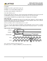
The ECP5 and ECP5-5G PLL contains an input mux to dynamically switch between two input reference clocks.
This mux is modeled by the PLLREFCS component. This mux may allow glitches and runt pulses through depend-
ing on when the clock is switched. It is expected that the input clocks have the same frequency. Table 22 defines
the I/O ports of the PLLREFCS block.
This component is instantiated in the PLL wrapper when the “Enable Clock Select” option is checked in the Clarity
Designer GUI. It can also be directly instantiated and software will automatically assign it to an unused PLL in
bypass mode and route the output to the CLKOP port.
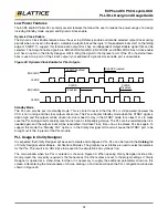
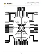
Figure 34. PLLREFCS Component Symbol
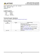
Table 21. PLLREFCS Component Port Definition
PLLREFCS Usage in VHDL
Component Declaration
COMPONENT PLLREFCS
PORT (
CLK0 : IN STD_LOGIC;
CLK1 : IN STD_LOGIC;
SEL : IN STD_LOGIC;
PLLCSOUT : OUT STD_LOGIC);
END COMPONENT;
PLLREFCS Instantiation
PLLREFCSInst0 : PLLREFCS
PORT MAP (
CLK0 => CLK_0
,CLK1 => CLK_1
,SEL => SELECT
,PLLCSOUT => CLK_OUT);
PLLREFCS Usage in Verilog
Component and Attribute Declaration
Port Name
Description
CLK0
CLK0
CLK1
CLK1
SEL
SEL = ‘0’, CLK0 is selected
SEL = ‘1’, CLK1 is selected
PLLCSOUT
PLLCSOUT
PLLREFCS
CLK0
CLK1
SEL
PLLCSOUT


