


ML610471/472/473/Q471/Q472/Q473 User's Manual
Chapter 17 RC Oscillation Type A/D Converter
17-15
(b)
32.768 kHz
c
Base clock
BSCLK
01H
RADMOD
(bits 4–0)
f
01H (ERAD=1)
RADCON
(bit 0)
g
(c)
00H
j
k
00H
(f)
12H
CR oscillating
state
(CROSC1)
Stop
Stop
Oscillates with RS1
Stop
(Counter A reference mode)
(Counter B reference mode)
0.366 sec
nA0·t
BSCLK
=nB0·t
RCCLK
(RS1)
nB0·tRCCLK(RT1)=nA1·t
BSCLK
(Increments by BSCLK)
CNTA2–0
0000H
(
Increments by BSCLK
)
nA1
0FB50H
d
(Increments by
RCCLK (RS1))
CNTB2–0
0000H
0000H
e
nB0
(Increments by
RCCLK (RT1))
10000H
−
nB0
INT generated
(a)
(d)
RC-ADC interrupt request
RADINT
(e)
l
h
HLT
Overflow
i
INT generated
<First Step>
<Second Step>
Note) nA0=4B0H, t
SYSCLK
=1/32768 Hz;
c
to
l
: Software processing; (a) to (f): Hardware processing
Overflow
00H
01H (ERAD=1)
Oscillates with RS1
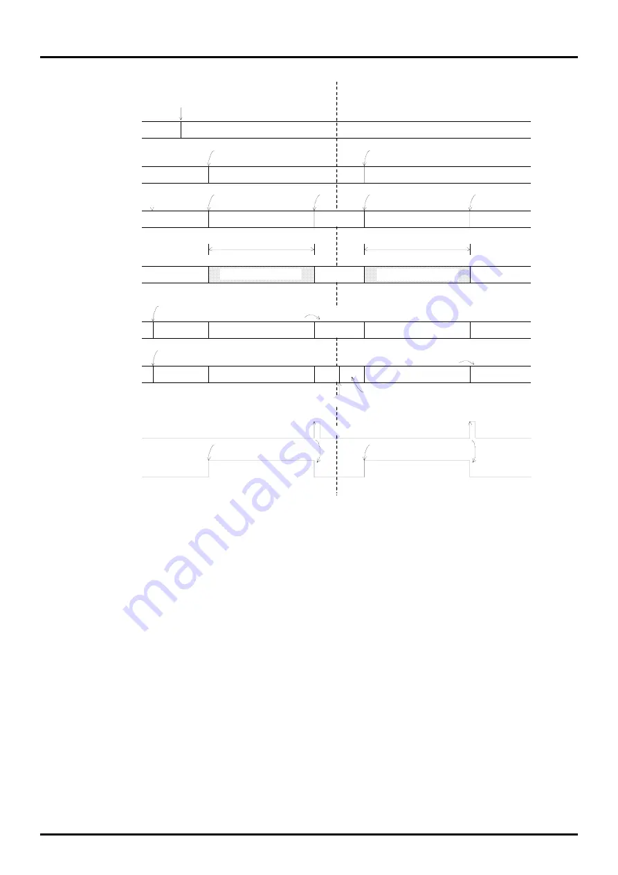
Figure 17-11 Timing Chart for 1 Cycle of A/D Conversion (Example)
<First step>
c
Set the base clock to 32.768 kHz. (Write “00H” in FCON0.)
d
Preset “10000H – nA0” in Counter A.
e
Preset “0000H” in Counter B.
f
Write “01H” in RADMOD to select Counter A reference mode and the oscillation mode that uses reference
resistance RS1.
g
Write “01H” in RADCON to start A/D conversion operation.
h
Write “1” in the HLT bit of SBYCON to set the device to HALT mode.
Note:
In this example, nA0 is set to 4B0H because the gate time “nA0 x t
BSCLK
” in oscillation mode with reference resistor RS1 is set to
0.366 second. The value of nA0 is related to how much the margin of the quantization error of the A/D conversion is: the greater
the nA0 value is, the smaller the margin of error becomes.
To reduce noise contamination to the RC oscillator circuit caused by CPU operation, it is recommended to constantly put the
device into HALT mode during operation of RC oscillation.
From this point of time, the RC oscillator circuit (RCOSC1) continues oscillation for about 0.366 second with the
reference resistance RS1. Then, when Counter A overflows, the RADINT signal is set to “1” and an RC-ADC interrupt
CNTA1-0
CNTB1-0
Summary of Contents for ML610471
Page 12: ...Chapter 1 Overview...
Page 38: ...Chapter 2 CPU and Memory Space...
Page 44: ...Chapter 3 Reset Function...
Page 48: ...Chapter 4 MCU Control Function...
Page 62: ...Chapter 5 Interrupts...
Page 82: ...Chapter 6 Clock Generation Circuit...
Page 94: ...Chapter 7 Time Base Counter...
Page 105: ...Chapter 8 Capture...
Page 114: ...Chapter 9 Timer...
Page 133: ...Chapter 10 Watchdog Timer...
Page 141: ...Chapter 11 UART...
Page 164: ...Chapter 12 Port 0...
Page 173: ...Chapter 13 Port 2...
Page 180: ...Chapter 14 Port 3...
Page 188: ...Chapter 15 Port 4...
Page 199: ...Chapter 16 Port 6...
Page 205: ...Chapter 17 RC Oscillation Type A D Converter...
Page 225: ...Chapter 18 LCD Drivers...
Page 243: ...Chapter 19 Power Supply Circuit...
Page 245: ...Chapter 20 uEASE Flash Writer System...
Page 249: ...Chapter 21 Software Development...
Page 258: ...Appendixes...
Page 280: ...Revision History...