4-1
4
4
Theory of Operation
4.1
INTRODUCTION
This section describes the theory of operation of the 4809A, 4819A, 4829A
and 4899A GPIB<->Modbus Controllers. The models are similar and have
a similar block diagram. Wherever the text refers to the Model 4899A, it
applies equally to the other models unless otherwise noted.
The Model 4819A and 4829A have some additional features and is covered
separately.
4.2
4899A AND 4809A BLOCK DIAGRAM DESCRIPTION
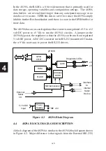
A block diagram of the 4899A is shown in Figure 4-1. The 4899A is a mi-
croprocessor based device that transparently passes data between the GPIB
(IEEE 488) bus and a Modbus slave device over a serial link. The 4899A
is made up of seven major elements, most of which are interconnected to
the microprocessor by a common data, address and control signal bus. The
4809A's block diagram is similar to the 4899A.
Incoming GPIB bus data and commands are received by the GPIB controller
chip. Each received character interrupts the microprocessor to place the
characters in the GPIB received data buffer. When a complete message
has been received, the parser checks the message for a valid command and
then acts upon it. Invalid messages cause a bit to be set in the unit's Event
Status Register and turn on the ERR LED.
If the message is a Modbus command then it is converted into a series of
binary characters to make up the Modbus RTU message packet. The Modbus
Summary of Contents for 4809A
Page 5: ...ii This page left intentionally blank...
Page 51: ...2 30 2 This page left intentionally blank...
Page 89: ...4 8 4 This page intentionally left blank...
Page 99: ...5 10 5 This page left intentionally blank...
Page 125: ...A 26 A3 This page intentionally left blank...
Page 131: ...I Index 6 This page left intentionally blank...

