


VDC for the “BIG STEP” PA Modules; +115 VDC and +60 VDC
for “BINARY” PA Modules; +115 VDC Driver Modules; and
+60 VDC for the Predriver Module.
The supplies then pass through RF chokes L1 and L2 and are
fused by F1 and F2. If a fuse for a half-quad opens (typically,
because of MOSFET failure), the other half-quad will continue
to operate. For modules used in a full-quad configuration, the
module will continue to deliver a reduced RF power level (at half
the peak-to-peak RF voltage across the combiner output trans-
former primary).
The drains of Q1/Q12 and Q2/Q9 are bypassed to ground by C1
and C3, and C2 and C4.
C.3.2
LED Indicators
Red LED indicators DS1 and DS2 illuminate if there is a blown
fuse on the module.
Green LED DS3 illuminates when the amplifier receives a turn-
on signal from the Modulation Encoder. The current for the LED
is derived from the rectified RF controlled by Q7 and Q8.
C.3.3
Cable Interlock
The cable interlock control signal from the Modulation Encoder
loops through the RF amplifier on pins P1-35/36 and P1-37/38.
The open fuse (Blown Fuse) indicators DS1 and DS2 are also
tied to this circuitry through diodes CR11 and CR12. If CR11 or
CR12 short, R16 and CR13 will clamp the supply voltage at +20
VDC.
Refer to SECTION L, Modulation Encoder, for a description of
the Cable Interlock and Blown Fuse Indication circuitry.
C.3.4
RF Drive
RF drive is fed to transformers T1 and T2. One RF drive trans-
former is used for each half-quad. RF drive for section A enters
the module at P1-49/50; RF drive for section B enters at P1-
53/54. Individual coaxial cables from the RF Drive Splitter feed
RF drive to the A and B section of each module so that if one
section fails the drive to the other section will not be affected. A
network in parallel with each RF drive transformer broadbands
the input circuit, so that no component changes are required for
operation at any frequency in the broadcast band. For T1, this
network consists of L3, R3, R22, and L6; for T2, the network
consists of L4, R4, R23, and L7.
Each RF drive transformer has two pairs of secondary windings,
which provide two pairs of drive signals, 180° out of phase, for
the upper and lower MOSFET pairs in each half-quad. On the
schematic diagram, small circles at one end of each transformer
winding indicate RF phasing.
Back-to-back zener diodes CR1, CR2, CR3, and CR4 protect the
MOSFET gates against overvoltages, including possible tran-
sient voltages.
When modules are used in the Power Amplifier stage, RF drive
is provided by the RF Drive Splitter. All RF drive cables are the
same length, so that RF drive phase is the same to all modules.
The RF amplifier schematic diagram indicates proper RF levels.
C.3.5
Control Section
Control signals enter at P1-45/46. Transistors Q5, Q6, Q7, and
Q8 are the ON-OFF control transistors for the module. For
modules used in the Driver stage, a “TTL HIGH” voltage at
P1-45/46 (+4 Volts or more) turns the amplifier OFF. A negative
voltage at P1-45/46 (-2 to -4 Volts) turns the amplifier ON.
For RF amplifiers used in the Power Amplifier stage, control
signals from the Modulation Encoder switch between “TTL
HIGH” and a small negative voltage to turn RF amplifier mod-
ules ON and OFF. The negative voltage is derived from the B-
supply output of the DC Regulator. Because the switching char-
acteristics of the modules change, depending on the number of
modules on at any instant, this voltage will vary with modulation
and change the turn-on and turn-off times of the modules.
For RF amplifiers used in the Driver stage, a fixed -5 VDC control
voltage from the Driver Encoder/Temp Sense Board keeps the
modules ON.
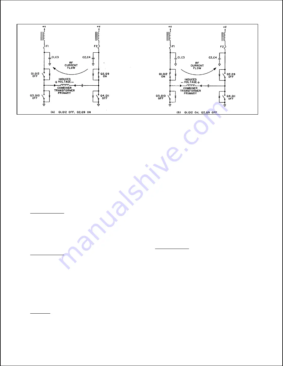
Figure C-5. RF Amplifier Module: Combiner Transformer
Primary Winding Current Flow With Module Off (817 2099 035)
DX-25U
C-4
888-2297-002
WARNING: Disconnect primary power prior to servicing.


