


MPC5553/MPC5554 Microcontroller Reference Manual, Rev. 5
25-62
Freescale Semiconductor
Using the read/write access registers (RWCS/RWA/RWD), memory-mapped e200z6 system bus resources
can be accessed through NZ6C3. The following subsections describe the steps which are required to access
memory-mapped resources.
NOTE
Read/write access can only access memory mapped resources when system
reset is de-asserted.
Misaligned accesses are NOT supported in the e200z6 Nexus3 module.
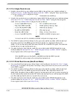
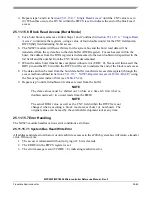
25.11.15.1 Single Write Access
1. Initialize the read/write access address register (RWA) through the access method outlined in
Section 25.11.10, “ NZ6C3 Register Access via JTAG / OnCE
” using the Nexus register index of
0x9 (see
). Configure as follows:
– Write Address
->
0xnnnnnnnn (write address)
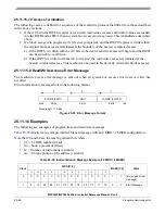
2. Initialize the read/write access control/status register (RWCS) through the access method outlined
Section 25.11.10, “ NZ6C3 Register Access via JTAG / OnCE
,” using the Nexus Register
). Configure the bits as follows:
– Access Control RWCS[AC]
–>
0b1 (to indicate start access)
– Map Select RWCS[MAP]
–>
0b000 (primary memory map)
– Access Priority RWCS[PR]
–>
0b00 (lowest priority)
– Read/Write RWCS[RW]
–>
0b1 (write access)
– Word Size RWCS[SZ]
–>
0b0xx (32-bit, 16-bit, 8-bit)
– Access Count RWCS[CNT]
–>
0x0000 or 0x0001 (single access)
NOTE
Access count RWCS[CNT] of 0x0000 or 0x0001 will perform a single
access.
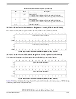
3. Initialize the read/write access data register (RWD) through the access method outlined in
Section 25.11.10, “ NZ6C3 Register Access via JTAG / OnCE
,” using the Nexus register index
– Write Data
->
0xnnnnnnnn (write data)
4. The NZ6C3 module will then arbitrate for the system bus and transfer the data value from the data
buffer RWD register to the memory mapped address in the read/write access address register
(RWA). When the access has completed without error (ERR=1’b0), NZ6C3 asserts the RDY
pin
and clears the DV bit in the RWCS register. This indicates that the device is ready for the next
access.
NOTE
Only the RDY pin as well as the DV and ERR bits within the RWCS provide
read/write access status to the external development tool.
Summary of Contents for MPC5553
Page 5: ...MPC5553 MPC5554 Microcontroller Reference Manual Rev 5 2 Freescale Semiconductor...
Page 21: ...MPC5553 MPC5554 Microcontroller Reference Manual Rev 5 xvi Freescale Semiconductor...
Page 47: ...MPC5553 MPC5554 Microcontroller Reference Manual Rev 5 1 26 Freescale Semiconductor...
Page 163: ...MPC5553 MPC5554 Microcontroller Reference Manual Rev 5 4 20 Freescale Semiconductor...
Page 179: ...MPC5553 MPC5554 Microcontroller Reference Manual Rev 5 5 16 Freescale Semiconductor...
Page 561: ...MPC5553 MPC5554 Microcontroller Reference Manual Rev 5 13 38 Freescale Semiconductor...
Page 615: ...MPC5553 MPC5554 Microcontroller Reference Manual Rev 5 14 54 Freescale Semiconductor...
Page 707: ...MPC5553 MPC5554 Microcontroller Reference Manual Rev 5 17 68 Freescale Semiconductor...
Page 755: ...MPC5553 MPC5554 Microcontroller Reference Manual Rev 5 18 48 Freescale Semiconductor...
Page 873: ...MPC5553 MPC5554 Microcontroller Reference Manual Rev 5 19 118 Freescale Semiconductor...
Page 984: ...MPC5553 MPC5554 Microcontroller Reference Manual Rev 5 Freescale Semiconductor 21 41...
Page 985: ...MPC5553 MPC5554 Microcontroller Reference Manual Rev 5 21 42 Freescale Semiconductor...
Page 1019: ...MPC5553 MPC5554 Microcontroller Reference Manual Rev 5 22 34 Freescale Semiconductor...
Page 1129: ...MPC5553 MPC5554 Microcontroller Reference Manual Rev 5 25 90 Freescale Semiconductor...


