background image

135

7679H–CAN–08/08

AT90CAN32/64/128

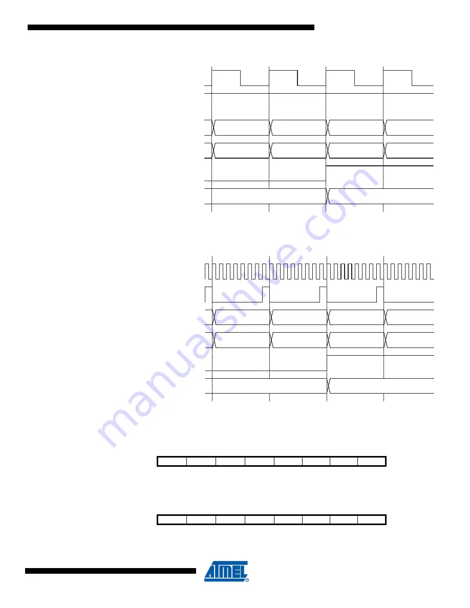
Figure 13-12.

Timer/Counter Timing Diagram, no Prescaling

Figure 13-13

 shows the same timing data, but with the prescaler enabled. 

Figure 13-13.

Timer/Counter Timing Diagram, with Prescaler (f

clk_I/O

/8)

13.11 16-bit Timer/Counter Register Description

13.11.1

Timer/Counter1 Control Register A – TCCR1A

13.11.2

Timer/Counter3 Control Register A – TCCR3A

TOVn 

(FPWM)

and ICFn 

(if used

as TOP)

OCRnx

(Update at TOP)

TCNTn

(CTC and FPWM)

TCNTn

(PC and PFC PWM)

TOP - 1

TOP

TOP - 1

TOP - 2

Old OCRnx Value

New OCRnx Value

TOP - 1

TOP

BOTTOM

1

clk

Tn

(clk

I/O

/1)

clk

I/O

TOVn 

(FPWM)

and ICFn 

(if used

as TOP)

OCRnx

(Update at TOP)

TCNTn

(CTC and FPWM)

TCNTn

(PC and PFC PWM)

TOP - 1

TOP

TOP - 1

TOP - 2

Old OCRnx Value

New OCRnx Value

TOP - 1

TOP

BOTTOM

1

clk

I/O

clk

Tn

(clk

I/O

/8)

Bit

7

6

5

4

3

2

1

0

COM1A1

COM1A0

COM1B1

COM1B0

COM1C1

COM1C0

WGM11

WGM10

TCCR1A

Read/Write

R/W

R/W

R/W

R/W

R/W

R/W

R/W

R/W

Initial Value

0

0

0

0

0

0

0

0

Bit

7

6

5

4

3

2

1

0

COM3A1

COM3A0

COM3B1

COM3B0

COM3C1

COM3C0

WGM31

WGM30

TCCR3A

Read/Write

R/W

R/W

R/W

R/W

R/W

R/W

R/W

R/W

Initial Value

0

0

0

0

0

0

0

0

Summary of Contents for AVR AT90CAN128

Page 1: ...ening Mode Spying or Autobaud Peripheral Features Programmable Watchdog Timer with On chip Oscillator 8 bit Synchronous Timer Counter 0 10 bit Prescaler External Event Counter Output Compare or 8 bit...

Page 2: ...Watchdog Timer with Internal Oscillator an SPI serial port IEEE std 1149 1 compliant JTAG test interface also used for accessing the On chip Debug system and programming and five software selectable...

Page 3: ...pplications The AT90CAN32 64 128 AVR is supported with a full suite of program and system development tools including C compilers macro assemblers program debugger simulators in circuit emula tors and...

Page 4: ...PROM SPI USART0 STATUS REGISTER Z Y X ALU PORTB DRIVERS PORTE DRIVERS PORTA DRIVERS PORTF DRIVERS PORTD DRIVERS PORTC DRIVERS PB7 PB0 PE7 PE0 PA7 PA0 PF7 PF0 RESET VCC AGND GND AREF XTAL1 XTAL2 CONTRO...

Page 5: ...PE6 ICP3 INT7 PE7 SS PB0 SCK PB1 MOSI PB2 MISO PB3 OC2A PB4 OC0A OC1C PB7 TOSC2 PG3 OC1B PB6 TOSC1 PG4 OC1A PB5 PC1 A9 T0 PD7 PC2 A10 PC3 A11 PC4 A12 PC5 A13 PC6 A14 PC7 A15 CLKO PA7 AD7 PG2 ALE PA6 A...

Page 6: ...C4 TCK PF5 ADC5 TMS PF6 ADC6 TDO AREF GND AVCC RXD0 PDI PE0 TXD0 PDO PE1 XCK0 AIN0 PE2 OC3A AIN1 PE3 OC3B INT4 PE4 OC3C INT5 PE5 T3 INT6 PE6 ICP3 INT7 PE7 SS PB0 SCK PB1 MOSI PB2 MISO PB3 OC2A PB4 OC0...

Page 7: ...oth high sink and source capability As inputs Port C pins that are externally pulled low will source current if the pull up resistors are activated The Port C pins are tri stated when a reset conditio...

Page 8: ...he functions of various special features of the AT90CAN32 64 128 as listed on page 88 1 6 10 RESET Reset input A low level on this pin for longer than the minimum pulse length will generate a reset Th...

Page 9: ...parate memories and buses for program and data Instructions in the program memory are executed with a single level pipelining While one instruction is being executed the next instruc tion is pre fetch...

Page 10: ...nter PC is stored on the Stack The Stack is effectively allocated in the general data SRAM and consequently the Stack size is only limited by the total SRAM size and the usage of the SRAM All user pro...

Page 11: ...application with the SEI and CLI instructions as described in the instruction set reference Bit 6 T Bit Copy Storage The Bit Copy instructions BLD Bit LoaD and BST Bit STore use the T bit as source or...

Page 12: ...e direct access to all registers and most of them are single cycle instructions As shown in Figure 3 2 each register is also assigned a data memory address mapping them directly into the first 32 loca...

Page 13: ...ch page in the program memory is accessed when the ELPM SPM instruction is used The different settings of the RAMPZ0 bit have the following effects AT90CAN32 and AT90CAN64 RAMPZ0 exists as register bi...

Page 14: ...tack Pointer is implemented as two 8 bit registers in the I O space The number of bits actually used is implementation dependent Note that the data space in some implementa tions of the AVR architectu...

Page 15: ...Control Register MCUCR Refer to Interrupts on page 60 for more information The Reset Vector can also be moved to the start of the Boot Flash section by programming the BOOTRST Fuse see Boot Loader Sup...

Page 16: ...even if it occurs simultaneously with the CLI instruction The following example shows how this can be used to avoid interrupts during the timed EEPROM write sequence When using the SEI instruction to...

Page 17: ...and this jump takes three clock cycles If an interrupt occurs during execution of a multi cycle instruction this instruction is completed before the interrupt is served If an interrupt occurs when th...

Page 18: ...ra tion of Boot Program section and associated Boot Lock bits for software protection are described in detail in Boot Loader Support Read While Write Self Programming on page 321 Memory Programming on...

Page 19: ...The lower data memory locations address both the Register File the I O memory Extended I O memory and the internal data SRAM The first 32 locations address the Register File the next 64 location the s...

Page 20: ...wait state one byte external access takes two three or four additional clock cycles for one two and three wait states respectively Interrupts subroutine calls and returns will need five seven or nine...

Page 21: ...rformed in two clkCPU cycles as described in Figure 4 3 Figure 4 3 On chip Data SRAM Access Cycles 32 Registers 64 I O Registers Internal SRAM ISRAM size 0x0000 0x001F 0x0020 0x005F XMem start ISRAM e...

Page 22: ...as minimum for the clock frequency used See Preventing EEPROM Corruption on page 26 for details on how to avoid problems in these situations In order to prevent unintentional EEPROM writes a specific...

Page 23: ...Enable The EEPROM Write Enable Signal EEWE is the write strobe to the EEPROM When address and data are correctly set up the EEWE bit must be written to one to write the value into the EEPROM The EEMWE...

Page 24: ...d for two cycles before the next instruction is executed Bit 0 EERE EEPROM Read Enable The EEPROM Read Enable Signal EERE is the read strobe to the EEPROM When the correct address is set up in the EEA...

Page 25: ...any ongoing SPM command to finish Assembly Code Example EEPROM_write Wait for completion of previous write sbic EECR EEWE rjmp EEPROM_write Set up address r18 r17 in address register out EEARH r18 out...

Page 26: ...ion can easily be avoided by following this design recommendation Keep the AVR RESET active low during periods of insufficient power supply voltage This can be done by enabling the internal Brown out...

Page 27: ...evices reserved bits should be written to zero if accessed Reserved I O memory addresses should never be written Some of the status flags are cleared by writing a logical one to them Note that unlike...

Page 28: ...cess is internal or external If the access is external the XMEM interface will output address data and the control signals on the ports according to Fig ure 4 6 this figure shows the wave forms withou...

Page 29: ...apacitive load Figure 4 5 External SRAM Connected to the AVR 4 5 4 Pull up and Bus keeper The pull ups on the AD7 0 ports may be activated if the corresponding Port register is written to one To reduc...

Page 30: ...the following figures are related to the internal system clock The skew between the internal and external clock XTAL1 is not guarantied varies between devices temperature and supply voltage Conse que...

Page 31: ...es the RAM internal or external Figure 4 9 External Data Memory Cycles with SRWn1 1 and SRWn0 1 1 Note 1 SRWn1 SRW11 upper sector or SRW01 lower sector SRWn0 SRW10 upper sector or SRW00 lower sector T...

Page 32: ...e sectors see Table 4 3 and Figure 4 4 By default the SRL2 SRL1 and SRL0 bits are set to zero and the entire external memory address space is treated as one sector When the entire SRAM address space i...

Page 33: ...bus keeper XMBK is not qualified with SRE so even if the XMEM interface is disabled the bus keepers are still activated as long as XMBK is one Bit 6 4 Reserved Bits These are reserved bits and will a...

Page 34: ...AM end for the external memory Addressing above address ISRAM end 0x8000 is not recommended since this will address an external mem ory location that is already accessed by another lower address To th...

Page 35: ...the following code examples Note 1 The example code assumes that the part specific header file is included Care must be exercised using this option as most of the memory is masked away Assembly Code E...

Page 36: ...General Purpose I O Register 0 GPIOR0 4 6 2 General Purpose I O Register 1 GPIOR1 4 6 3 General Purpose I O Register 2 GPIOR2 Bit 7 6 5 4 3 2 1 0 GPIOR07 GPIOR06 GPIOR05 GPIOR04 GPIOR03 GPIOR02 GPIOR...

Page 37: ...y the majority of the I O modules like Timer Counters SPI CAN USART The I O clock is also used by the External Interrupt module but note that some external interrupts are detected by asynchronous logi...

Page 38: ...ing stable Oscillator operation before instruction execution starts When the CPU starts from reset there is an additional delay allowing the power to reach a stable level before starting normal operat...

Page 39: ...tor values given by the manufacturer should be used For more information on how to choose capacitors and other details on Oscillator operation refer to the Multi purpose Oscillator Application Note Fi...

Page 40: ...EL Fuses to 0100 0101 0110 or 0111 The crystal should be connected as shown in Figure 5 3 Figure 5 3 Low frequency Crystal Oscillator Connections 12 22 pF capacitors may be necessary if the parasitic...

Page 41: ...C Oscillator At 5V and 25 C this calibration gives a fre quency within 10 of the nominal frequency Using calibration methods as described in application notes available at www atmel com avr it is poss...

Page 42: ...than 10 above the nominal fre quency Otherwise the EEPROM or Flash write may fail Note that the Oscillator is intended for calibration to 8 0 MHz Tuning to other values is not guaranteed as indicated...

Page 43: ...drive other circuits on the system The clock will be output also during reset and the normal operation of I O pin will be overridden when the fuse is pro grammed Any clock source including internal R...

Page 44: ...written to zero CLKPCE is cleared by hardware four cycles after it is written or when CLKPS bits are written Rewriting the CLKPCE bit within this time out period does neither extend the time out perio...

Page 45: ...gher frequency than the maximum frequency of the device at the present operating conditions The device is shipped with the CKDIV8 Fuse programmed Note The frequency of the asynchronous clock must be l...

Page 46: ...leep If a reset occurs during sleep mode the MCU wakes up and exe cutes from the Reset Vector Figure 5 1 on page 37 presents the different clock systems in the AT90CAN32 64 128 and their distribution...

Page 47: ...rements If the ADC is enabled a conversion starts automatically when this mode is entered Apart from the ADC Conversion Complete interrupt only an External Reset a Watchdog Reset a Brown out Reset a T...

Page 48: ...resonator selected as clock source 2 If AS2 bit in ASSR is set 3 Only INT3 0 or level interrupt INT7 4 6 6 Minimizing Power Consumption There are several issues to consider when trying to minimize the...

Page 49: ...start up time 6 6 5 Watchdog Timer If the Watchdog Timer is not needed in the application the module should be turned off If the Watchdog Timer is enabled it will be enabled in all sleep modes and he...

Page 50: ...pin is left floating when the JTAG interface is enabled while the JTAG TAP controller is not shifting data If the hardware connected to the TDO pin does not pull up the logic level power consumption w...

Page 51: ...er all reset sources have gone inactive a delay counter is invoked stretching the internal reset This allows the power to reach a stable level before normal operation starts The time out period of the...

Page 52: ...on Reset threshold voltage invokes the delay counter which determines how long the device is kept in RESET after MCU Status Register MCUSR Brown out Reset Circuit BODLEVEL 2 0 Delay Counters CKSEL 3...

Page 53: ...xternal Reset An External Reset is generated by a low level on the RESET pin Reset pulses longer than the minimum pulse width see Table 7 1 will generate a reset even if the clock is not running Short...

Page 54: ...ested down to VCC VBOT during the production test This guar antees that a Brown Out Reset will occur before VCC drops to a voltage where correct operation of the microcontroller is no longer guarantee...

Page 55: ...an tBOD given in Table 7 3 Figure 7 5 Brown out Reset During Operation 7 1 6 Watchdog Reset When the Watchdog times out it will generate a short reset pulse of one CK cycle duration On the falling edg...

Page 56: ...use of the Reset flags to identify a reset condition the user should read and then reset the MCUSR as early as possible in the program If the register is cleared before another reset occurs the source...

Page 57: ...the reset period expires without another Watchdog Reset the AT90CAN32 64 128 resets and executes from the Reset Vector For timing details on the Watchdog Reset refer to Table 7 6 on page 58 To prevent...

Page 58: ...c one must be writ ten to WDE even though it is set to one before the disable operation starts 2 Within the next four clock cycles write a logic 0 to WDE This disables the Watchdog In safety level 2 i...

Page 59: ...dure must be followed 1 In the same operation write a logic one to WDCE and WDE A logic one must be writ ten to WDE regardless of the previous value of the WDE bit 2 Within the next four clock cycles...

Page 60: ...0E INT6 External Interrupt Request 6 9 0x0010 INT7 External Interrupt Request 7 10 0x0012 TIMER2 COMP Timer Counter2 Compare Match 11 0x0014 TIMER2 OVF Timer Counter2 Overflow 12 0x0016 TIMER1 CAPT Ti...

Page 61: ...and general program setup for the Reset and Interrupt Vector Addresses in AT90CAN32 64 128 is Address Labels Code Comments 0x0000 jmp RESET Reset Handler 0x0002 jmp EXT_INT0 IRQ0 Handler 0x0004 jmp EX...

Page 62: ...IM3_CAPT Timer3 Capture Handler 0x0038 jmp TIM3_COMPA Timer3 CompareA Handler 0x003A jmp TIM3_COMPB Timer3 CompareB Handler 0x003C jmp TIM3_COMPC Timer3 CompareC Handler 0x003E jmp TIM3_OVF Timer3 Ove...

Page 63: ...h RAMEND Main program start 0x 01 out SPH r16 Set Stack Pointer to top of RAM 0x 02 ldi r16 low RAMEND 0x 03 out SPL r16 0x 04 sei Enable interrupts 0x 05 instr xxx When the BOOTRST Fuse is programmed...

Page 64: ...ge Enable IVCE bit to one 2 Within four cycles write the desired value to IVSEL while writing a zero to IVCE Interrupts will automatically be disabled while this sequence is executed Interrupts are di...

Page 65: ...e interrupts as explained in the IVSEL description above See Code Example below Assembly Code Example Move_interrupts Get MCUCR in r16 MCUCR mov r17 r16 Enable change of Interrupt Vectors ori r16 1 IV...

Page 66: ...the precise form must be used For example PORTB3 for bit no 3 in Port B here documented generally as PORTxn The physical I O Regis ters and bit locations are listed in Register Description for I O Por...

Page 67: ...s at the PINx I O address The DDxn bit in the DDRx Register selects the direction of this pin If DDxn is written logic one Pxn is configured as an output pin If DDxn is written logic zero Pxn is confi...

Page 68: ...ports Switching between input with pull up and output low generates the same problem The user must use either the tri state DDxn PORTxn 0b00 or the output high state DDxn PORTxn 0b11 as an intermedia...

Page 69: ...d by the two arrows tpd max and tpd min a single signal transition on the pin will be delayed between and 1 system clock period depending upon the time of assertion When reading back a software assign...

Page 70: ...power consumption if some input signals are left floating or have an analog signal level close to VCC 2 SLEEP is overridden for port pins enabled as external interrupt pins If the external interrupt r...

Page 71: ...n is to enable the internal pull up In this case the pull up will be disabled during reset If low power consumption during reset is important it is recommended to use an external pull up or pull down...

Page 72: ...ORTx REGISTER RPx READ PORTx PIN PUD PULLUP DISABLE clkI O I O CLOCK RDx READ DDRx D L Q Q SET CLR 0 1 0 1 0 1 DIxn AIOxn DIEOExn PVOVxn PVOExn DDOVxn DDOExn PUOExn PUOVxn PUOExn Pxn PULL UP OVERRIDE...

Page 73: ...e Output Driver is enabled the port value is controlled by the PVOV signal If PVOE is cleared and the Output Driver is enabled the port Value is controlled by the PORTxn Register bit PVOV Port Value O...

Page 74: ...rnal memory interface address 5 and Data 5 AD4 Port A Bit 4 AD4 External memory interface address 4 and Data 4 AD3 Port A Bit 3 AD3 External memory interface address 3 and Data 3 AD2 Port A Bit 2 AD2...

Page 75: ...OE SRE ADA 1 WR SRE ADA 1 WR SRE ADA 1 WR SRE ADA 1 WR PUOV 0 0 0 0 DDOE SRE SRE SRE SRE DDOV WR ADA WR ADA WR ADA WR ADA PVOE SRE SRE SRE SRE PVOV A7 ADA 1 D7 OUTPUT WR A6 ADA 1 D6 OUTPUT WR A5 ADA 1...

Page 76: ...mpare A The pin has to be configured as an output DDB5 set one to serve this function The OC1A pin is also the output pin for the PWM mode timer function OC2A Bit 4 OC2A Output Compare Match A output...

Page 77: ...figured as an input regardless of the setting of DDB0 As a slave the SPI is activated when this pin is driven low When the SPI is enabled as a master the data direction of this pin is controlled by DD...

Page 78: ...Signal Name PB3 MISO PB2 MOSI PB1 SCK PB0 SS PUOE SPE MSTR SPE MSTR SPE MSTR SPE MSTR PUOV PORTB3 PUD PORTB2 PUD PORTB1 PUD PORTB0 PUD DDOE SPE MSTR SPE MSTR SPE MSTR SPE MSTR DDOV 0 0 0 0 PVOE SPE M...

Page 79: ...0 A8 External memory interface address 8 Table 9 10 and Table 9 11 relate the alternate functions of Port C to the overriding signals shown in Figure 9 5 on page 72 Note 1 CKOUT is one if the CKOUT F...

Page 80: ...ctions in PC3 PC0 Signal Name PC3 A11 PC2 A10 PC1 A9 PC0 A8 PUOE SRE XMM 5 SRE XMM 6 SRE XMM 7 SRE XMM 7 PUOV 0 0 0 0 DDOE SRE XMM 5 SRE XMM 6 SRE XMM 7 SRE XMM 7 DDOV 1 1 1 1 PVOE SRE XMM 5 SRE XMM 6...

Page 81: ...ured as an input regardless of the value of DDD2 When the USART forces this pin to be an input the pull up can still be controlled by the PORTD2 bit INT1 SDA Port D Bit 1 INT1 External Interrupt sourc...

Page 82: ...ICP1 PUOE 0 RXCANEN TXCANEN 0 PUOV 0 PORTD6 PUD 0 0 DDOE 0 RXCANEN TXCANEN 0 DDOV 0 0 1 0 PVOE 0 0 TXCANEN UMSEL1 0 PVOV 0 0 XCK1 OUTPUT UMSEL1 TXCANEN TXCAN TXCANEN 0 PTOE 0 0 0 0 DIEOE 0 0 0 0 DIEOV...

Page 83: ...Timer Counter3 Output Compare B The pin has to be configured as an output DDE4 set one to serve this function The OC3B pin is also the output pin for the PWM mode timer function AIN1 OC3A Port E Bit...

Page 84: ...s data input line for the AT90CAN32 64 128 RXD0 USART0 Receive Pin Receive Data Data input pin for the USART0 When the USART0 receiver is enabled this pin is configured as an input regardless of the v...

Page 85: ...it 7 ADC7 Analog to Digital Converter input channel 7 Table 9 17 Overriding Signals for Alternate Functions in PE3 PE0 Signal Name PE3 AIN1 OC3A PE2 AIN0 XCK0 PE1 PDO TXD0 PE0 PDI RXD0 PUOE 0 0 TXEN0...

Page 86: ...alog to Digital Converter input channel 5 TMS JTAG Test mode Select This pin is used for navigating through the TAP controller state machine When the JTAG interface is enabled this pin can not be used...

Page 87: ...GEN JTAGEN JTAGEN JTAGEN DDOV 0 SHIFT_IR SHIFT_DR 0 0 PVOE JTAGEN JTAGEN JTAGEN JTAGEN PVOV 0 TDO 0 0 PTOE 0 0 0 0 DIEOE JTAGEN ADC7D JTAGEN ADC6D JTAGEN ADC5D JTAGEN ADC4D DIEOV JTAGEN 0 JTAGEN JTAGE...

Page 88: ...the AS2 bit in ASSR is set one to enable asyn chronous clocking of Timer Counter2 pin PG3 is disconnected from the port and becomes the inverting output of the Oscillator amplifier In this mode a Crys...

Page 89: ...0 DDOE AS2 DDOV 0 PVOE 0 PVOV 0 PTOE 0 DIEOE AS2 DIEOV EXCLK DI AIO T C2 OSC INPUT Table 9 23 Overriding Signals for Alternate Functions in PG3 0 Signal Name PG3 TOSC2 PG2 ALE PG1 RD PG0 WR PUOE AS2...

Page 90: ...ORTB5 PORTB4 PORTB3 PORTB2 PORTB1 PORTB0 PORTB Read Write R W R W R W R W R W R W R W R W Initial Value 0 0 0 0 0 0 0 0 Bit 7 6 5 4 3 2 1 0 DDB7 DDB6 DDB5 DDB4 DDB3 DDB2 DDB1 DDB0 DDRB Read Write R W...

Page 91: ...PIND4 PIND3 PIND2 PIND1 PIND0 PIND Read Write R W R W R W R W R W R W R W R W Initial Value N A N A N A N A N A N A N A N A Bit 7 6 5 4 3 2 1 0 PORTE7 PORTE6 PORTE5 PORTE4 PORTE3 PORTE2 PORTE1 PORTE0...

Page 92: ...ad Write R W R W R W R W R W R W R W R W Initial Value N A N A N A N A N A N A N A N A Bit 7 6 5 4 3 2 1 0 PORTG4 PORTG3 PORTG2 PORTG1 PORTG0 PORTG Read Write R R R R W R W R W R W R W Initial Value 0...

Page 93: ...of the start up time The start up time is defined by the SUT fuses as described in System Clock on page 37 If the level is sampled twice by the Watchdog Oscillator clock but disappears before the end...

Page 94: ...a level triggered interrupt will generate an interrupt request as long as the pin is held low Note 1 n 7 6 5 or 4 When changing the ISCn1 ISCn0 bits the interrupt must be disabled by clearing its Int...

Page 95: ...T7 0 pin triggers an interrupt request INTF7 0 becomes set one If the I bit in SREG and the corresponding interrupt enable bit INT7 0 in EIMSK are set one the MCU will jump to the interrupt vector The...

Page 96: ...implications for situations where a prescaled clock is used One example of prescaling arti facts occurs when the timer is enabled and clocked by the prescaler 6 CSn2 0 1 The number of system clock cy...

Page 97: ...pling the maximum frequency of an external clock it can detect is half the sampling fre quency Nyquist sampling theorem However due to variation of the system clock frequency and duty cycle caused by...

Page 98: ...without the risk of one of them advancing during con figuration When the TSM bit is written to zero the PSR2 and PSR310 bits are cleared by hardware and the Timer Counters start counting simultaneous...

Page 99: ...ccessing Timer Counter0 counter value and so on A lower case x replaces the Output Compare unit channel in this case A However when using the register or bit defines in a program the precise form must...

Page 100: ...nt will also set the Compare Flag OCF0A which can be used to generate an Output Compare interrupt request 12 2 2 Definitions The following definitions are used extensively throughout the section 12 3...

Page 101: ...es counts and how waveforms are generated on the Output Compare output OC0A For more details about advanced counting sequences and waveform generation see Modes of Operation on page 104 The Timer Coun...

Page 102: ...iting a one to the Force Output Compare FOC0A bit Forcing compare match will not set the OCF0A flag or reload clear the timer but the OC0A pin will be updated as if a real compare match had occurred t...

Page 103: ...n the figure are shown in bold Only the parts of the general I O port control regis ters DDR and PORT that are affected by the COM0A1 0 bits are shown When referring to the OC0A state the reference is...

Page 104: ...ter Timing Diagrams on page 108 12 7 1 Normal Mode The simplest mode of operation is the Normal mode WGM01 0 0 In this mode the counting direction is always up incrementing and no counter clear is per...

Page 105: ...of operation the TOV0 flag is set in the same timer clock cycle that the counter counts from MAX to 0x00 12 7 3 Fast PWM Mode The fast Pulse Width Modulation or fast PWM mode WGM01 0 3 provides a hig...

Page 106: ...k cycle the counter is cleared changes from MAX to BOTTOM The PWM frequency for the output can be calculated by the following equation The N variable represents the prescale factor 1 8 64 256 or 1024...

Page 107: ...the phase correct PWM mode is shown on Figure 12 7 The TCNT0 value is in the timing diagram shown as a histogram for illustrating the dual slope operation The diagram includes non inverted and inverte...

Page 108: ...te logic values 12 8 Timer Counter Timing Diagrams The Timer Counter is a synchronous design and the timer clock clkT0 is therefore shown as a clock enable signal in the following figures The figures...

Page 109: ...be set to zero when TCCR0A is written when operating in PWM mode When writing a logical one to the FOC0A bit an immediate com pare match is forced on the Waveform Generation unit The OC0A output is ch...

Page 110: ...R bit corresponding to the OC0A pin must be set in order to enable the output driver When OC0A is connected to the pin the function of the COM0A1 0 bits depends on the WGM01 0 bit setting Table 12 2 s...

Page 111: ...access both for read and write operations to the Timer Counter unit 8 bit counter Writing to the TCNT0 Register blocks removes the compare match on the following timer clock Modifying the counter TCNT...

Page 112: ...r TIFR0 12 9 5 Timer Counter0 Interrupt Flag Register TIFR0 Bit 1 OCF0A Output Compare Flag 0 A The OCF0A bit is set one when a compare match occurs between the Timer Counter0 and the data in OCR0A Ou...

Page 113: ...13 2 Overview Many register and bit references in this section are written in general form A lower case n replaces the Timer Counter number in this case 1 or 3 However when using the register or bit...

Page 114: ...terrupt requests abbreviated to Int Req in the figure signals are all visible in the Timer Interrupt Flag Register TIFRn All interrupts are individually masked with the Timer Interrupt Mask Register T...

Page 115: ...this case be double buffered allowing the TOP value to be changed in run time If a fixed TOP value is required the ICRn Register can be used as an alternative freeing the OCRnA to be used as PWM outpu...

Page 116: ...single 8 bit register for temporary storing of the high byte of the 16 bit access The same temporary register is shared between all 16 bit registers within each 16 bit timer Accessing the low byte tr...

Page 117: ...at accessing 16 bit registers are atomic operations If an interrupt occurs between the two instructions accessing the 16 bit register and the interrupt code updates the temporary register by accessing...

Page 118: ...embly code example returns the TCNTn value in the r17 r16 register pair Assembly Code Example 1 TIM16_ReadTCNTn Save global interrupt flag in r18 SREG Disable interrupts cli Read TCNTn into r17 r16 ld...

Page 119: ...omic operation described previously also applies in this case 13 4 Timer Counter Clock Sources The Timer Counter can be clocked by an internal or an external clock source The clock source is selected...

Page 120: ...value within one clock cycle via the 8 bit data bus It is important to notice that there are special cases of writing to the TCNTn Register when the counter is counting that will give unpredictable re...

Page 121: ...tly a part of the Input Capture unit are gray shaded Figure 13 3 Input Capture Unit Block Diagram Note The Analog Comparator Output ACO can only trigger the Timer Counter1 IC Unit not Timer Counter3 W...

Page 122: ...ator output ACO inputs are sampled using the same technique as for the Tn pin Figure 11 1 on page 97 The edge detector is also identical However when the noise canceler is enabled additional logic is...

Page 123: ...signals a match A match will set the Output Compare Flag OCFnx at the next timer clock cycle If enabled OCIEnx 1 the Output Com pare Flag generates an Output Compare interrupt The OCFnx flag is autom...

Page 124: ...od practice to read the low byte first as when accessing other 16 bit registers Writing the OCRnx Registers must be done via the TEMP Reg ister since the compare of all 16 bits is done continuously Th...

Page 125: ...Similarly do not write the TCNTn value equal to BOTTOM when the counter is downcounting The setup of the OCnx should be performed before setting the Data Direction Register for the port pin to output...

Page 126: ...bits have no effect on the Input Capture unit 13 8 2 Compare Output Mode and Waveform Generation The Waveform Generator uses the COMnx1 0 bits differently in normal CTC and PWM modes For all modes se...

Page 127: ...nytime The Input Capture unit is easy to use in Normal mode However observe that the maximum interval between the external events must not exceed the resolution of the counter If the interval between...

Page 128: ...the TOVn flag is set in the same timer clock cycle that the counter counts from MAX to 0x0000 13 9 3 Fast PWM Mode The fast Pulse Width Modulation or fast PWM mode WGMn3 0 5 6 7 14 or 15 provides a hi...

Page 129: ...A when used for defining the TOP value The ICRn Register is not double buffered This means that if ICRn is changed to a low value when the counter is running with none or a low prescaler value there i...

Page 130: ...bled in the fast PWM mode 13 9 4 Phase Correct PWM Mode The phase correct Pulse Width Modulation or phase correct PWM mode WGMn3 0 1 2 3 10 or 11 provides a high resolution phase correct PWM waveform...

Page 131: ...13 8 illustrates changing the TOP actively while the Timer Counter is running in the phase correct mode can result in an unsymmetrical output The reason for this can be found in the time of update of...

Page 132: ...inverting Compare Output mode the operation is inverted The dual slope operation gives a lower maximum operation fre quency compared to the single slope operation However due to the symmetric feature...

Page 133: ...OP works well when using fixed TOP values By using ICRn the OCRnA Register is free to be used for generating a PWM output on OCnA However if the base PWM frequency is actively changed by changing the...

Page 134: ...t and when the OCRnx Register is updated with the OCRnx buffer value only for modes utilizing double buffering Figure 13 10 shows a timing diagram for the setting of OCFnx Figure 13 10 Timer Counter T...

Page 135: ...C and FPWM TCNTn PC and PFC PWM TOP 1 TOP TOP 1 TOP 2 Old OCRnx Value New OCRnx Value TOP 1 TOP BOTTOM BOTTOM 1 clkTn clkI O 1 clkI O TOVn FPWM and ICFn if used as TOP OCRnx Update at TOP TCNTn CTC an...

Page 136: ...the WGMn3 0 bits setting Table 13 1 shows the COMnx1 0 bit functionality when the WGMn3 0 bits are set to a Normal or a CTC mode non PWM Table 13 2 shows the COMnx1 0 bit functionality when the WGMn3...

Page 137: ...to be used see Table 13 4 Modes of operation supported by the Timer Counter unit are Normal mode counter Clear Timer on Compare match CTC mode and three types of Pulse Width Modulation PWM modes See M...

Page 138: ...n1 PWMn1 WGMn0 PWMn0 Timer Counter Mode of Operation TOP Update of OCRnx at TOVn Flag Set on 0 0 0 0 0 Normal 0xFFFF Immediate MAX 1 0 0 0 1 PWM Phase Correct 8 bit 0x00FF TOP BOTTOM 2 0 0 1 0 PWM Pha...

Page 139: ...ility with future devices this bit must be written to zero when TCCRnB is written Bit 4 3 WGMn3 2 Waveform Generation Mode See TCCRnA Register description Bit 2 0 CSn2 0 Clock Select The three Clock S...

Page 140: ...re always read as zero 13 11 7 Timer Counter1 TCNT1H and TCNT1L 13 11 8 Timer Counter3 TCNT3H and TCNT3L The two Timer Counter I O locations TCNTnH and TCNTnL combined TCNTn give direct access both fo...

Page 141: ...is performed using an 8 bit temporary high byte register TEMP This temporary register is shared by all the other 16 bit registers See Accessing 16 bit Registers on page 116 Bit 7 6 5 4 3 2 1 0 OCR1A...

Page 142: ...ne and the I flag in the Status Register is set interrupts globally enabled the Timer Countern Input Capture interrupt is enabled The corresponding Interrupt Vector See Interrupts on page 60 is execut...

Page 143: ...Counter1 Interrupt Flag Register TIFR1 13 11 20 Timer Counter3 Interrupt Flag Register TIFR3 Bit 7 6 Reserved Bits These bits are reserved for future use Bit 5 ICFn Input Capture Flag This flag is set...

Page 144: ...NTn value matches the Output Compare Register A OCRnA Note that a Forced Output Compare FOCnA strobe will not set the OCFnA flag OCFnA is automatically cleared when the Output Compare Match A Interrup...

Page 145: ...n replaces the Timer Counter number in this case 2 However when using the register or bit defines in a program the precise form must be used i e TCNT2 for accessing Timer Counter2 counter value and so...

Page 146: ...increment or decrement its value The Timer Counter is inac tive when no clock source is selected The output from the Clock Select logic is referred to as the timer clock clkT2 The double buffered Outp...

Page 147: ...nit The main part of the 8 bit Timer Counter is the programmable bi directional counter unit Figure 14 2 shows a block diagram of the counter and its surrounding environment Figure 14 2 Counter Unit B...

Page 148: ...ator continuously compares TCNT2 with the Output Compare Register OCR2A Whenever TCNT2 equals OCR2A the comparator signals a match A match will set the Output Compare Flag OCF2A at the next timer cloc...

Page 149: ...ches for one timer clock cycle there are risks involved when changing TCNT2 when using the Output Compare channel independently of whether the Timer Counter is running or not If the value written to T...

Page 150: ...tells the Waveform Generator that no action on the OC2A Register is to be performed on the next compare match For compare output actions in the non PWM modes refer to Table 14 2 on page 158 For fast P...

Page 151: ...Timer on Compare or CTC mode WGM21 0 2 the OCR2A Register is used to manipulate the counter resolution In CTC mode the counter is cleared to zero when the counter value TCNT2 matches the OCR2A The OCR...

Page 152: ...s cleared on the compare match between TCNT2 and OCR2A and set at BOTTOM In inverting Compare Output mode the output is set on compare match and cleared at BOTTOM Due to the single slope operation the...

Page 153: ...l on each compare match COM2A1 0 1 The waveform generated will have a maximum frequency of foc2A fclk_I O 2 when OCR2A is set to zero This feature is similar to the OC2A toggle in CTC mode except the...

Page 154: ...e PWM frequency for the output when using phase correct PWM can be calcu lated by the following equation The N variable represents the prescale factor 1 8 32 64 128 256 or 1024 The extreme values for...

Page 155: ...l In asynchronous mode clkI O should be replaced by the Timer Counter Oscillator clock The figures include information on when interrupt flags are set Figure 14 9 contains timing data for basic Timer...

Page 156: ...6 7679H CAN 08 08 AT90CAN32 64 128 Figure 14 11 Timer Counter Timing Diagram Setting of OCF2A with Prescaler fclk_I O 8 OCFnx OCRnx TCNTn OCRnx Value OCRnx 1 OCRnx OCRnx 1 OCRnx 2 clkI O clkTn clkI O...

Page 157: ...utput is changed according to its COM2A1 0 bits setting Note that the FOC2A bit is implemented as a strobe Therefore it is the value present in the COM2A1 0 bits that determines the effect of the forc...

Page 158: ...1 0 bits are set to a normal or CTC mode non PWM Table 14 3 shows the COM2A1 0 bit functionality when the WGM21 0 bits are set to fast PWM mode Note 1 A special case occurs when OCR2A equals TOP and C...

Page 159: ...duces a risk of missing a compare match between TCNT2 and the OCR2A Register 14 9 3 Output Compare Register A OCR2A Table 14 4 Compare Output Mode Phase Correct PWM Mode 1 COM2A1 COM2A0 Description 0...

Page 160: ...corrupted Bit 2 TCN2UB Timer Counter2 Update Busy When Timer Counter2 operates asynchronously and TCNT2 is written this bit becomes set When TCNT2 has been updated from the temporary storage register...

Page 161: ...erwise the MCU will enter sleep mode before the changes are effective This is particularly important if the Output Compare2 interrupt is used to wake up the device since the Output Compare function is...

Page 162: ...During asynchronous operation the synchronization of the interrupt flags for the asynchronous timer takes 3 processor cycles plus one timer cycle The timer is therefore advanced by at least one before...

Page 163: ...TOIE2A Timer Counter2 Overflow Inter rupt Enable and TOV2 are set one the Timer Counter2 Overflow interrupt is executed In PWM mode this bit is set when Timer Counter2 changes counting direction at 0...

Page 164: ...14 11 1 General Timer Counter Control Register GTCCR Bit 1 PSR2 Prescaler Reset Timer Counter2 When this bit is one the Timer Counter2 prescaler will be reset This bit is normally cleared immediately...

Page 165: ...Timer Counters see 16 bit Timer Counter Timer Counter1 and Timer Counter3 on page 113 and 8 bit Timer Counter0 with PWM on page 99 Figure 15 1 Output Compare Modulator Block Diagram When the modulator...

Page 166: ...h toggle Compare Output mode COMnx1 0 1 Figure 15 3 Output Compare Modulator Timing Diagram In this example Timer Counter0 provides the carrier while the modulating signal is generated by the Output C...

Page 167: ...er of system clock cycles of one period of the carrier OC0A In this example the resolution is reduced by a factor of two The reason for the reduction is illustrated in Figure 15 3 at the second and th...

Page 168: ...wing features 16 1 Features Full duplex Three wire Synchronous Data Transfer Master or Slave Operation LSB First or MSB First Data Transfer Seven Programmable Bit Rates End of Transmission Interrupt F...

Page 169: ...packet by pulling high the Slave Select SS line The last incoming byte will be kept in the Buffer Register for later use When configured as a Slave the SPI interface will remain sleeping with MISO tr...

Page 170: ...omatic port overrides refer to Alternate Port Functions on page 71 Note 1 See Alternate Functions of Port B on page 76 for a detailed description of how to define the direction of the user defined SPI...

Page 171: ...c header file is included Assembly Code Example 1 SPI_MasterInit Set MOSI and SCK output all others input ldi r17 1 DD_MOSI 1 DD_SCK out DDR_SPI r17 Enable SPI Master set clock rate fck 16 ldi r17 1 S...

Page 172: ...onfigured so by the user All other pins are inputs When SS is driven high all pins are inputs and the SPI is passive which Assembly Code Example 1 SPI_SlaveInit Set MISO output all others input ldi r1...

Page 173: ...ve As a result of the SPI becoming a Slave the MOSI and SCK pins become inputs 2 The SPIF flag in SPSR is set and if the SPI interrupt is enabled and the I bit in SREG is set the interrupt routine wil...

Page 174: ...gure 16 4 for an example The CPOL functionality is summarized below Bits 1 0 SPR1 SPR0 SPI Clock Rate Select 1 and 0 These two bits control the SCK rate of the device configured as a Master SPR1 and S...

Page 175: ...SPI is in Master mode see Table 16 4 This means that the minimum SCK period will be two CPU clock periods When the SPI is configured as Slave the SPI is only guaranteed to work at fclkio 4 or lower Th...

Page 176: ...0 CPOL 0 CPHA 1 Setup Rising Sample Falling 1 CPOL 1 CPHA 0 Sample Falling Setup Rising 2 CPOL 1 CPHA 1 Setup Falling Sample Rising 3 Bit 1 Bit 6 LSB MSB SCK CPOL 0 mode 0 SAMPLE I MOSI MISO CHANGE 0...

Page 177: ...it Detection and Digital Low Pass Filter Three Separate Interrupts on TX Complete TX Data Register Empty and RX Complete Multi processor Communication Mode Double Speed Asynchronous Communication Mode...

Page 178: ...tor and Control logic for handling different serial frame for mats The write buffer allows a continuous transfer of data without any delay between frames The Receiver is the most complex part of the U...

Page 179: ...al Signal Used for synchronous slave operation xn cko Clock output to XCK pin Internal Signal Used for synchronous master operation fclkio System I O Clock frequency 17 4 1 Internal Clock Generation B...

Page 180: ...er that the Receiver will in this case only use half the number of samples reduced from 16 to 8 for data sampling and clock recovery and therefore a more accurate baud rate setting and system clock ar...

Page 181: ...led at falling XCKn edge If UCPOLn is set the data will be changed at falling XCKn edge and sampled at rising XCKn edge 17 5 Serial Frame A serial frame is defined to be one character of data bits wit...

Page 182: ...lculated by doing an exclusive or of all the data bits If odd parity is used the result of the exclusive or is inverted The relation between the parity bit and data bits is as follows Peven Parity bit...

Page 183: ...ese types of applications the initialization code can be placed directly in the main routine or be combined with initialization code for other I O modules 17 7 Data Transmission USART Transmitter The...

Page 184: ...e following code examples show a simple USART0 transmit function based on polling of the Data Register Empty UDRE0 flag When using frames with less than eight bits the most signif icant bits written t...

Page 185: ...ninth bit can be used for indicating an address frame when using multi processor communi cation mode or for other protocol handling as for example synchronization 17 7 3 Transmitter Flags and Interru...

Page 186: ...rrupts are enabled When the transmit complete interrupt is used the interrupt han dling routine does not have to clear the TXCn flag this is done automatically when the interrupt is executed 17 7 4 Pa...

Page 187: ...ceiving Frames with 9 Data Bits If 9 bit characters are used UCSZn 7 the ninth bit must be read from the RXB8n bit in UCS RnB before reading the low bits from the UDRn This rule applies to the FEn DOR...

Page 188: ...de Example 1 USART0_Receive Wait for data to be received lds r18 UCSR0A sbrs r18 RXC0 rjmp USART0_Receive Get status and 9th bit then data from buffer lds r17 UCSR0B lds r16 UDR0 If error return 1 and...

Page 189: ...ed in the receive buffer The FEn flag is zero when the stop bit was correctly read as one and the FEn flag will be one when the stop bit was incorrect zero This flag can be used for detecting out of s...

Page 190: ...le shows how to flush the receive buffer Note 1 The example code assumes that the part specific header file is included 17 9 Asynchronous Data Reception The USARTn includes a clock recovery and a data...

Page 191: ...clock is synchronized to the start bit the data recovery can begin The data recovery unit uses a state machine that has 16 states for each bit in Normal mode and eight states for each bit in Double Sp...

Page 192: ...frames at too fast or too slow bit rates or the internally generated baud rate of the Receiver does not have a similar see Table 17 2 base frequency the Receiver will not be able to synchronize the fr...

Page 193: ...nction of incoming frames received by the USARTn Receiver Frames that do not contain address information will be ignored and not put into the receive buffer This effectively reduces the number of inco...

Page 194: ...e set to use a 9 bit charac ter frame format The following procedure should be used to exchange data in Multi processor Communication mode 1 All Slave MCUs are in Multi processor Communication mode MP...

Page 195: ...gister when the Shift Register is empty Then the data will be serially transmitted on the TxDn pin The receive buffer consists of a two level FIFO The FIFO will change its state whenever the receive b...

Page 196: ...detected A Data OverRun occurs when the receive buffer is full two characters it is a new character waiting in the Receive Shift Register and a new start bit is detected This bit is valid until the re...

Page 197: ...En Flags Bit 3 TXENn Transmitter Enable Writing this bit to one enables the USARTn Transmitter The Transmitter will override normal port operation for the TxDn pin when enabled The disabling of the Tr...

Page 198: ...hin each frame The Receiver will generate a parity value for the incoming data and compare it to the UPMn0 setting If a mismatch is detected the UPEn Flag in UCSRnA will be set Bit 3 USBSn Stop Bit Se...

Page 199: ...nd UBRR1H Table 17 7 UCSZn Bits Settings UCSZn2 UCSZn1 UCSZn0 Character Size 0 0 0 5 bit 0 0 1 6 bit 0 1 0 7 bit 0 1 1 8 bit 1 0 0 Reserved 1 0 1 Reserved 1 1 0 Reserved 1 1 1 9 bit Table 17 8 UCPOLn...

Page 200: ...et baud rate are bold in the table Higher error ratings are acceptable but the Receiver will have less noise resistance when the error ratings are high especially for large serial frames see Asynchron...

Page 201: ...0 51 0 2 103 0 2 95 0 0 191 0 0 9600 23 0 0 47 0 0 25 0 2 51 0 2 47 0 0 95 0 0 14 4k 15 0 0 31 0 0 16 2 1 34 0 8 31 0 0 63 0 0 19 2k 11 0 0 23 0 0 12 0 2 25 0 2 23 0 0 47 0 0 28 8k 7 0 0 15 0 0 8 3 5...

Page 202: ...0 2 259 0 2 143 0 0 287 0 0 9600 51 0 2 103 0 2 64 0 2 129 0 2 71 0 0 143 0 0 14 4k 34 0 8 68 0 6 42 0 9 86 0 2 47 0 0 95 0 0 19 2k 25 0 2 51 0 2 32 1 4 64 0 2 35 0 0 71 0 0 28 8k 16 2 1 34 0 8 21 1...

Page 203: ...207 0 2 416 0 1 9600 77 0 2 155 0 2 95 0 0 191 0 0 103 0 2 207 0 2 14 4k 51 0 2 103 0 2 63 0 0 127 0 0 68 0 6 138 0 1 19 2k 38 0 2 77 0 2 47 0 0 95 0 0 51 0 2 103 0 2 28 8k 25 0 2 51 0 2 31 0 0 63 0 0...

Page 204: ...ocontroller applications The TWI protocol allows the systems designer to interconnect up to 128 different devices using only two bi directional bus lines one for clock SCL and one for data SDA The onl...

Page 205: ...d Frame Format 18 3 1 Transferring Bits Each data bit transferred on the TWI bus is accompanied by a pulse on the clock line The level of the data line must be stable when the clock line is high The o...

Page 206: ...000 is reserved for a general call When a general call is issued all slaves should respond by pulling the SDA line low in the ACK cycle A general call is used when a master wishes to transmit the sam...

Page 207: ...t for the slave or the slave needs extra time for processing between the data transmissions The slave extending the SCL low period will not affect the SCL high period which is determined by the master...

Page 208: ...ith the shortest high period The low period of the combined clock is equal to the low period of the master with the longest low period Note that all masters listen to the SCL line effectively starting...

Page 209: ...This implies that in multi master systems all data transfers must use the same composi tion of SLA R W and data packets In other words All transmissions must contain the same number of data packets o...

Page 210: ...the slave must be at least 16 times higher than the SCL frequency Note that slaves may prolong the SCL low period thereby reducing the average TWI bus clock period The SCL frequency is generated accor...

Page 211: ...the General Call address Upon an address match the Control Unit is informed allowing correct action to be taken The TWI may or may not acknowledge its address depending on settings in the TWCR The Add...

Page 212: ...INT flag is set the SCL low period is stretched The TWINT flag must be cleared by software by writing a logic one to it Note that this flag is not automati cally cleared by hardware when executing the...

Page 213: ...TWEN bit enables TWI operation and activates the TWI interface When TWEN is written to one the TWI takes control over the I O pins connected to the SCL and SDA pins enabling the slew rate limiters and...

Page 214: ...tion no data is lost in the transition from Master to Slave Handling of the ACK bit is controlled automatically by the TWI logic the CPU cannot access the ACK bit directly Bits 7 0 TWD TWI Data Regist...

Page 215: ...n interface to the TWI hardware In this example a master wishes to transmit a single data byte to a slave This description is quite abstract a more detailed explanation follows later in this section A...

Page 216: ...outine Assuming that the status code is as expected the application must load a data packet into TWDR Subsequently a specific value must be written to TWCR instructing the TWI hardware to transmit the...

Page 217: ...heck value of TWI Status Register Mask prescaler bits If status different from START go to ERROR ldi r16 SLA_W sts TWDR r16 ldi r16 1 TWINT 1 TWEN sts TWCR r16 TWDR SLA_W TWCR 1 TWINT 1 TWEN Load SLA_...

Page 218: ...e Address In Figure 18 12 to Figure 18 18 circles are used to indicate that the TWINT flag is set The num bers in the circles show the status code held in TWSR with the prescaler bits masked to zero A...

Page 219: ...propriate action to be taken for each of these status codes is detailed in Table 18 3 When SLA W has been successfully transmitted a data packet should be transmitted This is done by writing the data...

Page 220: ...itted and TWSTO flag will be reset 0x20 SLA W has been transmitted NOT ACK has been received Load data byte or No TWDR action or No TWDR action or No TWDR action 0 1 0 1 0 0 1 1 1 1 1 1 X X X X Data b...

Page 221: ...cessfull transmission to a slave receiver Next transfer started with a repeated start condition Not acknowledge received after the slave address Not acknowledge received after a data byte Arbitration...

Page 222: ...be 0x08 See Table 18 3 In order to enter MR mode SLA R must be transmitted This is done by writing SLA R to TWDR Thereafter the TWINT bit should be cleared by writing it to one to continue the transf...

Page 223: ...alue 1 X 1 0 X 1 0 X S SLA R A DATA A 0x08 0x40 0x50 SLA R 0x10 A P 0x48 A or A 0x38 Other master continues 0x38 Other master continues W A 0x68 Other master continues 0x78 0xB0 To corresponding state...

Page 224: ...d not addressed slave mode will be entered A START condition will be transmitted when the bus becomes free 0x40 SLA R has been transmitted ACK has been received No TWDR action or No TWDR action 0 0 0...

Page 225: ...tes 0x68 and 0x78 If the TWEA bit is reset during a transfer the TWI will return a Not Acknowledge 1 to SDA after the next received data byte This can be used to indicate that the slave is not able to...

Page 226: ...ssed slave mode own SLA will be recognized GCA will be recognized if TWGCE 1 Switched to the not addressed slave mode no recognition of own SLA or GCA a START condition will be transmitted when the bu...

Page 227: ...of the general call address and one or more data bytes Last data byte received is not acknowledged n From master to slave From slave to master Any number of data bytes and their associated acknowledge...

Page 228: ...the TWI will operate in ST mode otherwise SR mode is entered After its own slave address and the write bit have been received the TWINT flag is set and a valid status code can be read from TWSR The st...

Page 229: ...Arbitration lost in SLA R W as mas ter own SLA R has been received ACK has been returned Load data byte or Load data byte X X 0 0 1 1 0 1 Last data byte will be transmitted and NOT ACK should be recei...

Page 230: ...are affected The SDA and SCL lines are released and no STOP condition is transmitted S SLA R A DATA A 0xA8 0xB8 A 0xB0 Reception of the own slave address and one or more data bytes Last data byte tra...

Page 231: ...MR mode Thus the transfer direction must be changed The master must keep control of the bus during all these steps and the steps should be carried out as an atomical operation If this principle is vio...

Page 232: ...rection bit In this case arbitration will occur either in the READ WRITE bit or in the data bits The masters trying to output a one on SDA while another master outputs a zero will lose the arbitration...

Page 233: ...be released and not addressed slave mode will be entered A START condition will be transmitted when the bus becomes free No Arbitration lost in Data Direction Yes Write Data byte will be received and...

Page 234: ...entifier Mask rev 2 0 B 8 Bytes Data Buffer Static Allocation Tx Rx Frame Buffer or Automatic Reply Configuration Time Stamping 1 Mbit s Maximum Transfer Rate at 8 MHz TTC Timer Listening Mode for Spy...

Page 235: ...icate the number of following data bytes in the Data field In a remote frame the DLC contains the number of requested data bytes The Data field that follows can hold up to 8 data bytes The frame integ...

Page 236: ...an error 2 0B Passive Ignores 29 bit ID messages 2 0B Active Handles both 11 and 29 bit ID Messages 19 2 3 CAN Bit Timing To ensure correct sampling up to the last bit a CAN node needs to re synchroni...

Page 237: ...rors This segment may be lengthened during re synchronization 19 2 3 5 Sample Point The sample point is the point of time at which the bus level is read and interpreted as the value of the respective...

Page 238: ...aracteristics to suit the bus Early sampling allows more Time Quanta in the Phase Segment 2 so the Synchronization Jump Width can be programmed to its maximum This maximum capacity to shorten or lengt...

Page 239: ...19 2 5 2 Error at Bit Level Monitoring The ability of the transmitter to detect errors is based on the monitoring of bus signals Each node which transmits also observes the bus level and thus detects...

Page 240: ...ssage objects the message is stored and the application is informed by interrupt Another advantage is that incoming remote frames can be answered automatically by the full CAN controller with the corr...

Page 241: ...le RXCAN input pin freezes TEC and REC error counters Figure 19 6 Listening Mode 19 4 2 Bit Timing FSM s Finite State Machine of the CAN channel need to be synchronous to the time quantum So the input...

Page 242: ...compensate The baud rate selection is made by Tbit calculation Tbit 1 Tsyns Tprs Tphs1 Tphs2 1 Tsyns 1 x Tscl BRP 5 0 1 clkIO 1TQ 2 Tprs 1 to 8 x Tscl PRS 2 0 1 x Tscl 3 Tphs1 1 to 8 x Tscl PHS1 2 0 1...

Page 243: ...a CAN frame descriptor It contains all information to handle a CAN frame This means that a MOb has been outlined to allow to describe a CAN message like an object The set of MObs is the front end part...

Page 244: ...e CAN channel scans all the MObs in Tx configuration finds the MOb having the highest priority and tries to send it 4 When the transmission is completed the TXOK flag is set interrupt 5 All the parame...

Page 245: ...r the reply 3 When the transmission of the reply is completed the TXOK flag is set interrupt 4 All the parameters and data are available in the MOb until a new initialization 19 5 2 5 Frame Buffer Rec...

Page 246: ...e page number is the MOb number This page number is set in CANPAGE register The number 15 is reserved for factory tests CANHPMOB register gives the MOb having the highest priority in CANSIT registers...

Page 247: ...vided by 8 It provides clkCANTIM frequency to the CAN Timer if the CAN controller is enabled TclkCANTIM TclkIO x 8 x CANTCON 7 0 1 19 6 2 16 bit Timer This timer starts counting from 0x0000 when the C...

Page 248: ...re 19 12 Line Error Mode Note More than one REC TEC change may apply during a given message transfer 19 7 2 Error Types BERR Bit error The bit value which is monitored is different from the bit value...

Page 249: ...sends an error frame on network If the CAN channel detects an error frame on network it sends its own error frame 19 8 Interrupts 19 8 1 Interrupt organization The different interrupts are Interrupt o...

Page 250: ...ese interrupt flags writing a logical zero doesn t change the interrupt flag value OVRTIM interrupt flag is reset as the other interrupt sources of CANGIT register and is also reset entering in its de...

Page 251: ...ata Index ID Tag 2 ID Tag 1 ID Tag 4 ID Tag 3 ID Mask 2 ID Mask 1 ID Mask 4 ID Mask 3 Time Stamp Low Time Stamp High Message Data MOb Status MOb Control DLC Page MOb MOb0 ID Tag 2 MOb0 ID Tag 1 MOb0 I...

Page 252: ...e traced observing OVFG in CANGSTA register c f Figure 19 9 on page 243 Bit 5 TTC Time Trigger Communication 0 no TTC 1 TTC mode Bit 4 SYNTTC Synchronization of TTC This bit is only used in TTC mode 0...

Page 253: ...enable mode The CAN channel enters in enable mode once 11 recessive bits has been read Bit 0 SWRES Software Reset Request This auto resettable bit only resets the CAN controller 0 no reset 1 reset th...

Page 254: ...CAN controller interrupts except for OVRTIM interrupt This bit can be used for polling method Bit 6 BOFFIT Bus Off Interrupt Flag Writing a logical one resets this interrupt flag BOFFIT flag is only s...

Page 255: ...ons of the fixed form in the CRC delimiter acknowledgment delimiter or EOF Bit 0 AERG Acknowledgment Error General Writing a logical one resets this interrupt flag 0 no interrupt 1 acknowledgment erro...

Page 256: ...t provides the availability of the MOb It is set to one when the MOb is enabled i e CONMOB1 0 of CANCDMOB register Once TXOK or RXOK is set to one TXOK for automatic reply the corresponding ENMOB is r...

Page 257: ...er 1 CANBT1 Bit 7 Reserved Bit This bit is reserved for future use For compatibility with future devices it must be written to zero when CANBT1 is written Bit 6 1 BRP5 0 Baud Rate Prescaler Bit 7 6 5...

Page 258: ...mp width defines the maximum number of clock cycles A bit period may be shortened or lengthened by a re synchronization Bit 4 Reserved Bit This bit is reserved for future use For compatibility with fu...

Page 259: ...red sampling point SP again at one TclkIO clock before SP and finally at SP Then the bit level will be determined by a majority vote of the three samples SMP 1 configuration is not compatible with BRP...

Page 260: ...its can be pre programmed to match with the wanted configuration of the CANPAGE register i e AINC and INDX2 0 setting 19 10 17 CAN Page MOb Register CANPAGE Bit 7 6 5 4 3 2 1 0 TIMTTC7 TIMTTC6 TIMTTC5...

Page 261: ...the corresponding ENMOB bit of CANEN registers is cleared When the controller is ready to send a frame if two or more message objects are enabled as producers the lower MOb index is supplied first Bi...

Page 262: ...OB bit of CANEN regis ters is not cleared The next matching frame will update the CERR flag Bit 1 FERR Form Error This flag can generate an interrupt It must be cleared using a read modify write softw...

Page 263: ...3 0 DLC3 0 Data Length Code Number of Bytes in the data field of the message DLC field of the remote or data frame to send The range of DLC is from 0 up to 8 If DLC field 8 then effective DLC 8 This f...

Page 264: ...s it must be written to zero when CANIDTn are written When a remote or data frame is received this bit does not operate in the comparison but it is updated with un predicted values Bit 0 RB0TAG Reserv...

Page 265: ...d Bit This bit is reserved for future use For compatibility with future devices it must be written to zero when CANIDTn are written Bit 0 IDEMSK Identifier Extension Mask 0 comparison true forced 1 bi...

Page 266: ...is byte is equal to the specified message location of the pre defined identifier index If auto incrementation is used at the end of the data register writ ing or reading cycle the index is auto increm...

Page 267: ...1 0x0E 0x04 0x13 200 75 0 3125 16 7 4 4 1 0x08 0x0C 0x37 0 625 8 3 2 2 1 0x12 0x04 0x13 125 75 0 500 16 7 4 4 1 0x0E 0x0C 0x37 1 000 8 3 2 2 1 0x1E 0x04 0x13 100 75 0 625 16 7 4 4 1 0x12 0x0C 0x37 1...

Page 268: ...33 12 5 3 3 1 0x02 0x08 0x25 0 500 8 3 2 2 1 0x04 0x04 0x13 200 80 0 333333 15 7 4 3 1 0x02 0x0C 0x35 0 500 10 4 3 2 1 0x04 0x06 0x23 125 75 0 500 16 7 4 4 1 0x04 0x0C 0x37 1 000 8 3 2 2 1 0x0A 0x04 0...

Page 269: ...ator Block Diagram 1 2 Notes 1 ADC multiplexer output see Table 20 2 on page 271 2 Refer to Figure 1 2 on page 5 or Figure 1 3 on page 6 and Table 9 15 on page 83 for Analog Comparator pin placement 2...

Page 270: ...pt mode defined by ACIS1 and ACIS0 The Analog Comparator interrupt routine is executed if the ACIE bit is set and the I bit in SREG is set ACI is cleared by hardware when executing the corresponding i...

Page 271: ...consequently the ADC must be switched off to utilize this feature If the Analog Comparator Multiplexer Enable bit ACME in ADCSRB is set and the ADC is switched off ADEN in ADCSRA is zero MUX2 0 in ADM...

Page 272: ...e AIN1 0 pin is disabled The corre sponding PIN Register bit will always read as zero when this bit is set When an analog signal is applied to the AIN1 0 pin and the digital input from this pin is not...

Page 273: ...ntial voltage input combinations Two of the differential inputs ADC1 ADC0 and ADC3 ADC2 are equipped with a programmable gain stage providing amplification steps of 0 dB 1x 20 dB 10x or 46 dB 200x on...

Page 274: ...C MULTIPLEXER SELECT ADMUX ADC CTRL ST ATUS REGISTER ADCSRA ADC DATA REGISTER ADCH ADCL MUX2 ADIE ADATE ADSC ADEN ADIF ADIF MUX1 MUX0 ADPS0 ADPS1 ADPS2 MUX3 CONVERSION LOGIC 10 BIT DAC SAMPLE HOLD COM...

Page 275: ...er is updated and the result from the conversion is lost When ADCH is read ADC access to the ADCH and ADCL Registers is re enabled The ADC has its own interrupt which can be triggered when a conversio...

Page 276: ...the conversion was started 21 4 Prescaling and Conversion Timing Figure 21 3 ADC Prescaler By default the successive approximation circuitry requires an input clock frequency between 50 kHz and 200 kH...

Page 277: ...uto Triggering is used the prescaler is reset when the trigger event occurs This assures a fixed delay from the trigger event to the start of conversion In this mode the sample and hold takes place tw...

Page 278: ...me as a single ended conversion 13 ADC clock cycles from the next prescaled clock cycle A conversion initiated by the user when CKADC2 is high will take 14 ADC clock cycles due to the synchronization...

Page 279: ...reference selection is continuously updated until a conversion is started Once the conversion starts the channel and reference selection is locked to ensure a sufficient sampling time for the ADC Con...

Page 280: ...from the internal bandgap reference VBG through an internal amplifier In either case the external AREF pin is directly connected to the ADC and the reference voltage can be made more immune to noise b...

Page 281: ...capacitor through the series resistance combined resistance in the input path The ADC is optimized for analog signals with an output impedance of approximately 10 k or less If such a source is used th...

Page 282: ...ements as much as possible The remaining offset in the analog path can be measured directly by selecting the same channel for both differential inputs This offset residue can be then subtracted in sof...

Page 283: ...eal transition at 1 5 LSB below maximum Ideal value 0 LSB Figure 21 11 Gain Error Integral Non linearity INL After adjusting for offset and gain error the INL is the maximum deviation of an actual tra...

Page 284: ...des a range of input voltages 1 LSB wide will code to the same value Always 0 5 LSB Absolute Accuracy The maximum deviation of an actual unadjusted transition compared to an ideal transition for any c...

Page 285: ...selected voltage reference The result is presented in two s complement form from 0x200 512d through 0x1FF 511d Note that if the user wants to perform a quick polarity check of the result it is suffici...

Page 286: ...reference left adjusted result Voltage on ADC3 is 300 mV voltage on ADC2 is 500 mV ADCR 512 1 300 500 2560 41 0x029 ADCL will thus read 0x40 and ADCH will read 0x0A Writing zero to ADLAR right adjust...

Page 287: ...affect the ADC Data Register immediately regardless of any ongoing conver sions For a complete description of this bit see The ADC Data Register ADCL and ADCH on page 290 Bits 4 0 MUX4 0 Analog Channe...

Page 288: ...N A ADC0 ADC0 10x 01001 ADC1 ADC0 10x 01010 ADC0 ADC0 200x 01011 ADC1 ADC0 200x 01100 ADC2 ADC2 10x 01101 ADC3 ADC2 10x 01110 ADC2 ADC2 200x 01111 ADC3 ADC2 200x 10000 ADC0 ADC1 1x 10001 ADC1 ADC1 1x...

Page 289: ...DATE ADC Auto Trigger Enable When this bit is written to one Auto Triggering of the ADC is enabled The ADC will start a con version on a positive edge of the selected trigger signal The trigger source...

Page 290: ...it is sufficient to read ADCH Otherwise ADCL must be read first then ADCH The ADLAR bit in ADMUX and the MUXn bits in ADMUX affect the way the result is read from the registers If ADLAR is set the re...

Page 291: ...red the ADTS2 0 settings will have no effect A conversion will be triggered by the rising edge of the selected interrupt flag Note that switching from a trig ger source that is cleared to a trigger so...

Page 292: ...abled The corresponding PIN Register bit will always read as zero when this bit is set When an analog signal is applied to the ADC7 0 pin and the digital input from this pin is not needed this bit sho...

Page 293: ...the sections JTAG Programming Overview on page 352 and Boundary scan IEEE 1149 1 JTAG on page 300 respectively The On chip Debug support is considered being private JTAG instructions and dis tributed...

Page 294: ...R is cleared the TAP input signals are internally pulled high and the JTAG is enabled for Boundary scan and program ming In this case the TAP output pin TDO is left floating in states where the JTAG T...

Page 295: ...ICATION INTERFACE BREAKPOINT UNIT FLOW CONTROL UNIT OCD STATUS AND CONTROL INTERNAL SCAN CHAIN M U X INSTRUCTION REGISTER ID REGISTER BYPASS REGISTER JTAG PROGRAMMING INTERFACE PC Instruction Address...

Page 296: ...0 at the rising edges of TCK to enter the Shift Instruction Register Shift IR state While in this state shift the four bits of the JTAG instructions into the JTAG Instruction Register from the TDI in...

Page 297: ...gisters and some JTAG instructions may select certain func tions to be performed in the Run Test Idle making it unsuitable as an Idle state Note Independent of the initial state of the TAP Controller...

Page 298: ...embler and C programs compiled with third party vendors compilers AVR Studio runs under Microsoft Windows 95 98 2000 NT XP For a full description of the AVR Studio please refer to the AVR Studio User...

Page 299: ...pins that need to be controlled observed to perform JTAG program ming in addition to power pins It is not required to apply 12V externally The JTAGEN Fuse must be programmed and the JTD bit in the MC...

Page 300: ...instruction It may be desirable to have the AVR device in reset during test mode If not reset inputs to the device may be deter mined by the scan operations and the internal software may be in an unde...

Page 301: ...of the component The relevant version number is shown in Table 23 1 23 3 2 2 Part Number The part number is a 16 bit code identifying the component The JTAG Part Number for AT90CAN32 64 128 is listed...

Page 302: ...the logic levels on the dig ital I O pins as well as the boundary between digital and analog logic for analog circuitry having off chip connections See Boundary scan Chain on page 304 for a complete d...

Page 303: ...ampled into the Boundary scan Chain Shift DR The IDCODE scan chain is shifted by the TCK input 23 4 3 SAMPLE_PRELOAD 0x2 Mandatory JTAG instruction for pre loading the output latches and taking a snap...

Page 304: ...logic one in the JTAG Reset Register selected by the JTAG instruction AVR_RESET This bit is reset by a Power on Reset or by writing a logic zero to the flag 23 6 Boundary scan Chain The Boundary scan...

Page 305: ...nected outside the dotted box in Figure 23 4 to make the scan chain read the actual pin value For Analog function there is a direct connection from the external pin to the analog circuit and a scan ch...

Page 306: ...dinary scan support for digital port pins suffice for connectivity tests The only reason for having TWIEN in the scan path is to be able to disconnect the slew rate control buffer when doing boundary...

Page 307: ...table by fuses These are Internal RC Oscilla tor External Clock High Frequency Crystal Oscillator Low frequency Crystal Oscillator and Ceramic Resonator Figure 23 7 shows how each oscillator with exte...

Page 308: ...because the system logic can disable clock options in sleep modes thereby disconnecting the Oscillator pins from the scan path if not provided 23 6 5 Scanning the Analog Comparator The relevant Compa...

Page 309: ...E input Turns off Analog Comparator when true 1 Depends upon C code being executed ACO output Analog Comparator Output Will become input to C code being executed 0 ACME input Uses output signal from A...

Page 310: ...ll analog inputs are shared with a digital port pin as well Figure 23 10 Analog to Digital Converter The signals are described briefly in Table 23 7 AREF PRECH DACOUT COMP MUXEN_7 ADC_7 MUXEN_6 ADC_6...

Page 311: ...0 0 ADCEN Input Power on signal to the ADC 0 0 AMPEN Input Power on signal to the gain stages 0 0 DAC_9 Input Bit 9 of digital value to DAC 1 1 DAC_8 Input Bit 8 of digital value to DAC 0 0 DAC_7 Inp...

Page 312: ...x bit 3 0 0 MUXEN_2 Input Input Mux bit 2 0 0 MUXEN_1 Input Input Mux bit 1 0 0 MUXEN_0 Input Input Mux bit 0 1 1 NEGSEL_2 Input Input Mux for negative input for differential signal bit 2 0 0 NEGSEL_1...

Page 313: ...rify the output from the comparator to be high The ADC need not be used for pure connectivity testing since all analog inputs are shared with a digital port pin as well When using the ADC remember the...

Page 314: ...when the Boundary scan chain is selected as data path Bit 0 is the LSB the first bit scanned in and the first bit scanned out The scan order follows the pin out order as far as possible Therefore the...

Page 315: ...scan Order Bit Number Signal Name Comment Module 200 AC_IDLE Comparator 199 ACO 198 ACME 197 AINBG 196 COMP ADC 195 ACLK 194 ACTEN 193 PRIVATE_SIGNAL 1 192 ADCBGEN 191 ADCEN 190 AMPEN 189 DAC_9 188 D...

Page 316: ...e 148 PE3 Data 147 PE3 Control 146 PE3 Pullup_Enable 145 PE4 Data 144 PE4 Control 143 PE4 Pullup_Enable 142 PE5 Data 141 PE5 Control 140 PE5 Pullup_Enable 139 PE6 Data 138 PE6 Control 137 PE6 Pullup_E...

Page 317: ...112 PB7 Data 111 PB7 Control 110 PB7 Pullup_Enable 109 PG3 Data Port G 108 PG3 Control 107 PG3 Pullup_Enable 106 PG4 Data 105 PG4 Control 104 PG4 Pullup_Enable 103 PRIVATE_SIGNAL 1 102 RSTT Observe On...

Page 318: ...73 PD6 Control 72 PD6 Pullup_Enable 71 PD7 Data 70 PD7 Control 69 PD7 Pullup_Enable 68 PG0 Data Port G 67 PG0 Control 66 PG0 Pullup_Enable 65 PG1 Data 64 PG1 Control 63 PG1 Pullup_Enable 62 PC0 Data...

Page 319: ...ullup_Enable 35 PA7 Data Port A 34 PA7 Control 33 PA7 Pullup_Enable 32 PA6 Data 31 PA6 Control 30 PA6 Pullup_Enable 29 PA5 Data 28 PA5 Control 27 PA5 Pullup_Enable 26 PA4 Data 25 PA4 Control 24 PA4 Pu...

Page 320: ...eration software The order and function of bits in the Boundary scan Data Register are included in this description A BSDL file for AT90CAN32 64 128 is available 12 PA0 Pullup_Enable Port A 11 PF3 Dat...

Page 321: ...341 used during programming The page organization does not affect normal operation 24 2 Application and Boot Loader Flash Sections The Flash memory is organized in two main sections the Application s...

Page 322: ...oing programming the software must ensure that the RWW section never is being read If the user software is trying to read code that is located inside the RWW section i e by a call jmp lpm or an interr...

Page 323: ...ile Write vs No Read While Write Read While Write RWW Section No Read While Write NRWW Section Z pointer Addresses RWW Section Z pointer Addresses NRWW Section CPU is Halted During the Operation Code...

Page 324: ...000 Flashend Program Memory BOOTSZ 11 Application Flash Section Boot Loader Flash Section Flashend Program Memory BOOTSZ 10 0x0000 Program Memory BOOTSZ 01 Program Memory BOOTSZ 00 Application Flash S...

Page 325: ...ection Modes Application Section 1 Lock Bit Mode BLB02 BLB01 Protection 1 1 1 No restrictions for SPM or LPM accessing the Application section 2 1 0 SPM is not allowed to write to the Application sect...

Page 326: ...128 and always read as zero Bit 4 RWWSRE Read While Write Section Read Enable When programming Page Erase or Page Write to the RWW section the RWW section is blocked for reading the RWWSB will be set...

Page 327: ...r with either RWWSRE BLBSET PGWRT or PGERS the following SPM instruction will have a spe cial meaning see description above If only SPMEN is written the following SPM instruction will store the value...

Page 328: ...in a page by page fashion Before programming a page with the data stored in the temporary page buffer the page must be erased The temporary page buffer is filled one word at a time using SPM and the...

Page 329: ...ent of PCWORD in the Z register is used to address the data in the temporary buffer The temporary buffer will auto erase after a Page Write operation or by writing the RWWSRE bit in SPMCSR It is also...

Page 330: ...SPM instruction is executed within four cycles after BLBSET and SPMEN are set in SPMCSR The Z pointer is don t care during this operation but for future compatibility it is recommended to load the Z...

Page 331: ...e read as zero Fuse and Lock bits that are unprogrammed will be read as one 24 7 10 Preventing Flash Corruption During periods of low VCC the Flash program can be corrupted because the supply voltage...

Page 332: ...rogramming Page Erase and Page Write registers used r0 r1 temp1 r16 temp2 r17 looplo r24 loophi r25 spmcsrval r20 storing and restoring of registers is not included in the routine register usage can b...

Page 333: ...ubi for PAGESIZEB 256 brne Rdloop return to RWW section verify that RWW section is safe to read Return in temp1 SPMCSR sbrs temp1 RWWSB If RWWSB is set the RWW section is not ready yet ret re enable t...

Page 334: ...0x37FF 0x3800 0 0 4096 words 32 0x0000 0x2FFF 0x3000 0x3FFF 0x2FFF 0x3000 AT90CAN64 1 1 512 words 4 0x0000 0x7DFF 0x7E00 0x7FFF 0x7DFF 0x7E00 1 0 1024 words 8 0x0000 0x7BFF 0x7C00 0x7FFF 0x7BFF 0x7C0...

Page 335: ...ring PAGE WRITE operation AT90CAN64 PCMSB 14 Most significant bit in the program counter The program counter is 15 bits PC 14 0 PAGEMSB 6 Most significant bit which is used to address the words within...

Page 336: ...ramming mode The Fuse bits are locked in both Serial and Parallel Programming mode 1 3 0 0 Further programming and verification of the Flash and EEPROM is disabled in Parallel and Serial Programming m...

Page 337: ...M executing from the Application section is not allowed to read from the Boot Loader section If Interrupt Vectors are placed in the Application section interrupts are disabled while executing from the...

Page 338: ...utput on Port PC7 See Clock Output Buffer on page 43 for details 4 See System Clock Prescaler on page 44 for details The status of the Fuse bits is not affected by Chip Erase Note that the Fuse bits a...

Page 339: ...wise noted 25 5 1 Signal Names In this section some pins of the AT90CAN32 64 128 are referenced by signal names describing their functionality during parallel programming see Figure 25 1 and Table 25...

Page 340: ...ng 1 Device is ready for new command OE PD2 I Output Enable Active low WR PD3 I Write Pulse Active low BS1 PD4 I Byte Select 1 0 selects low byte 1 selects high byte XA0 PD5 I XTAL Action Bit 0 XA1 PD...

Page 341: ...0 1000 Read Signature bytes and Calibration byte 0000 0100 Read Fuse and Lock bits 0000 0010 Read Flash 0000 0011 Read EEPROM Table 25 11 No of Words in a Page and No of Pages in the Flash Device Flas...

Page 342: ...needs only be loaded before programming or reading a new 256 word window in Flash or 256 byte EEPROM This consideration also applies to Signature bytes reading 25 6 3 Chip Erase The Chip Erase will er...

Page 343: ...sitive pulse This latches the data bytes See Figure 25 3 for signal waveforms F Repeat B through E until the entire buffer is filled or until all data within the page is loaded While the lower bits in...

Page 344: ...AGE and PCWORD are listed in Table 25 11 on page 341 Figure 25 3 Programming the Flash Waveforms 1 Note 1 XX is don t care The letters refer to the programming description above PROGRAM MEMORY WORD AD...

Page 345: ...r is filled L Program EEPROM page 1 Set BS1 to 0 2 Give WR a negative pulse This starts programming of the EEPROM page RDY BSY goes low 3 Wait until to RDY BSY goes high before programming the next pa...

Page 346: ...RDY BSY to go high 25 6 9 Programming the Fuse High Bits The algorithm for programming the Fuse High bits is as follows refer to Programming the Flash on page 342 for details on Command and Data load...

Page 347: ...and Lock Bits The algorithm for reading the Fuse and Lock bits is as follows refer to Programming the Flash on page 342 for details on Command loading 1 A Load Command 0000 0100 2 Set OE to 0 BS2 to...

Page 348: ...1 25 7 SPI Serial Programming Overview This section describes how to serial program and verify Flash Program memory EEPROM Data memory Memory Lock bits and Fuse bits in the AT90CAN32 64 128 25 7 1 Sig...

Page 349: ...les for fck 12 MHz 3 CPU clock cycles for fck 12 MHz High 2 CPU clock cycles for fck 12 MHz 3 CPU clock cycles for fck 12 MHz 25 7 2 Pin Mapping 25 7 3 Parameters The Flash parameters are given in Tab...

Page 350: ...e by supplying the address and data together with the appropriate Write instruction An EEPROM memory location is first automatically erased before new data is written If polling is not used the user m...

Page 351: ...High Byte o data out i data in x don t care Instruction Instruction Format 1 Operation 1 Byte 1 Byte 2 2 Byte 3 Byte4 Programming Enable 1010 1100 0101 0011 xxxx xxxx xxxx xxxx Enable Serial Programm...

Page 352: ...its 1010 1100 111x xxxx xxxx xxxx 11ii iiii Write Lock bits Set bits 0 to program Lock bits See Table 25 1 on page 336 for details Read Signature Byte 0011 0000 000x xxxx xxxx xxbb oooo oooo Read Sign...

Page 353: ...he JTAG instructions useful for programming are listed below The OPCODE for each instruction is shown behind the instruction name in hex format The text describes which data register is selected as pa...

Page 354: ...command Update DR The programming command is applied to the Flash inputs Run Test Idle One clock cycle is generated executing the applied command not always required see Table 25 16 below 25 9 1 4 PRO...

Page 355: ...h Data Byte Register 25 9 2 1 Reset Register The Reset Register is a Test Data Register used to reset the part during programming It is required to reset the part before entering Programming mode A hi...

Page 356: ...address high bits b address low bits H 0 Low byte 1 High Byte o data out i data in x don t care Instruction TDI Sequence 1 2 TDO Sequence 1 2 Notes 1a Chip Erase 0100011_10000000 0110001_10000000 011...

Page 357: ...4f Write EEPROM Page 0110011_00000000 0110001_00000000 0110011_00000000 0110011_00000000 xxxxxxx_xxxxxxxx xxxxxxx_xxxxxxxx xxxxxxx_xxxxxxxx xxxxxxx_xxxxxxxx 3 4g Poll for Page Write Complete 0110011_...

Page 358: ...1_00000100 xxxxxxx_xxxxxxxx 8b Read Extended Fuse Byte 8 0111010_00000000 0111011_00000000 xxxxxxx_xxxxxxxx xxxxxxx_oooooooo 8c Read Fuse High Byte 9 0111110_00000000 0111111_00000000 xxxxxxx_xxxxxxxx...

Page 359: ...it mapping for Fuses Extended byte is listed in Table 25 3 on page 337 9 The bit mapping for Fuses High byte is listed in Table 25 4 on page 337 10 The bit mapping for Fuses Low byte is listed in Tabl...

Page 360: ...matically alternates between writing the low and the high byte for each new Update DR state starting with the low byte for the first Update DR encountered after entering the PROG_PAGELOAD command The...

Page 361: ...ion transparently for the user However if too few bits are shifted between each Update DR state during page load the TAP controller should stay in the Run Test Idle state for some TCK cycles to ensure...

Page 362: ...ddress within one page and must be written as 0 4 Enter JTAG instruction PROG_PAGELOAD 5 Load the entire page by shifting in all instruction words in the page byte by byte start ing with the LSB of th...

Page 363: ...ing instruction 4g or wait for tWLRH refer to Table 26 15 on page 382 9 Repeat steps 3 to 8 until all data have been programmed Note that the PROG_PAGELOAD instruction can not be used when programming...

Page 364: ...struction 8f To only read Extended Fuse byte use programming instruction 8b To only read Fuse High byte use programming instruction 8c To only read Fuse Low byte use programming instruction 8d To only...

Page 365: ...t dam age to the device This is a stress rating only and functional operation of the device at these or other conditions beyond those indicated in the operational sections of this specification is not...

Page 366: ...mA VCC 5V IOL 10 mA VCC 3V 0 7 0 5 V VOH Output High Voltage 4 Ports A B C D E F G IOH 20 mA VCC 5V IOH 10 mA VCC 3V 4 2 2 4 V IIL Input Leakage Current I O Pin VCC 5 5V pin low absolute value 1 0 A...

Page 367: ...at VCC 3V under steady state conditions non transient the following must be observed TQFP and QFN Package 1 The sum of all IOH for all ports should not exceed 400 mA 2 The sum of all IOH for ports A0...

Page 368: ...a maximum frequency of 8 MHz requires VCC 2 7V Figure 26 2 Maximum Frequency vs VCC AT90CAN32 64 128 tCLCX Low Time 50 25 ns tCLCH Rise Time 1 6 0 5 s tCHCL Fall Time 1 6 0 5 s tCLCL Change in period...

Page 369: ...n to VILmax 10 pF Cb 400 pF 3 20 0 1Cb 3 2 250 ns tSP 1 Spikes Suppressed by Input Filter 0 50 2 ns Ii Input Current each I O Pin 0 1 VCC Vi 0 9 VCC 10 10 A Ci 1 Capacitance for each I O Pin 10 pF fSC...

Page 370: ...uirement will not be strictly met for fSCL 308 kHz when fCK 8 MHz Still AT90CAN32 64 128 devices connected to the bus may communicate at full speed 400 kHz with other AT90CAN32 64 128 devices as well...

Page 371: ...irements Slave Mode 13 Setup Slave 10 ns 14 Hold Slave tck 15 SCK to out Slave 15 16 SCK to SS high Slave 20 17 SS high to tri state Slave 10 18 SS low to SCK Slave 2 tck Table 26 4 SPI Timing Paramet...

Page 372: ...teristics for CAN physical layer have not yet been finalized 2 Metastable immunity flip flop Table CAN Physical Layer Characteristics 1 Parameter Condition Min Max Units 1 TxCAN output delay Vcc 2 7 V...

Page 373: ...e Ended Conversion VREF 4V Vcc 4V ADC clock 1 MHz Noise Reduction Mode LSB Integral Non linearity INL Single Ended Conversion VREF 4V Vcc 4V ADC clock 200 kHz 0 5 1 LSB Differential Non linearity DNL...

Page 374: ...x or 200x VREF 4V Vcc 5V ADC clock 50 200 kHz 0 5 1 LSB Gain Error Gain 1x 10x or 200x 2 0 2 LSB Offset Error Gain 1x 10x or 200x VREF 4V Vcc 5V ADC clock 50 200 kHz 1 0 1 LSB Clock Frequency Free Run...

Page 375: ...alid to RD Low 115 1 0 tCLCL 10 ns 6 tAVWL Address Valid to WR Low 115 1 0 tCLCL 10 ns 7 tLLWL ALE Low to WR Low 47 5 67 5 0 5 tCLCL 15 2 0 5 tCLCL 5 2 ns 8 tLLRL ALE Low to RD Low 47 5 67 5 0 5 tCLCL...

Page 376: ...ta Hold After WR High 240 2 0 tCLCL 10 ns 15 tDVWH Data Valid to WR High 375 3 0 tCLCL ns 16 tWLWH WR Pulse Width 365 3 0 tCLCL 10 ns Table 26 11 External Data Memory Characteristics VCC 2 7 5 5 Volts...

Page 377: ...mbol Parameter 4 MHz Oscillator Variable Oscillator Unit Min Max Min Max 0 1 tCLCL Oscillator Frequency 0 0 8 MHz 10 tRLDV Read Low to Data Valid 440 2 0 tCLCL 60 ns 12 tRLRH RD Pulse Width 485 2 0 tC...

Page 378: ...16 tWLWH WR Pulse Width 735 3 0 tCLCL 15 ns Table 26 14 External Data Memory Characteristics VCC 2 7 5 5 Volts SRWn1 1 SRWn0 1 Continued Symbol Parameter 4 MHz Oscillator Variable Oscillator Unit Min...

Page 379: ...Write Read WR T5 A15 8 Address Prev addr DA7 0 Address Data Prev data XX RD DA7 0 XMBK 0 Data Address System Clock CLKCPU 1 4 2 7 6 3a 3b 5 8 12 16 13 10 11 14 15 9 T4 ALE T1 T2 T3 Write Read WR T6 A1...

Page 380: ...Programming Characteristics Figure 26 10 Parallel Programming Timing Including some General Timing Requirements ALE T1 T2 T3 Write Read WR T7 A15 8 Address Prev addr DA7 0 Address Data Prev data XX RD...

Page 381: ...g Timing Reading Sequence within the Same Page with Timing Requirements 1 XTAL1 PAGEL tPLXH XLXH t tXLPH ADDR0 Low Byte DATA Low Byte DATA High Byte ADDR1 Low Byte DATA BS1 XA0 XA1 LOAD ADDRESS LOW BY...

Page 382: ...Low to XTAL1 High 200 ns tXHXL XTAL1 Pulse Width High 150 ns tXLDX Data and Control Hold after XTAL1 Low 67 ns tXLWL XTAL1 Low to WR Low 0 ns tXLPH XTAL1 Low to PAGEL high 0 ns tPLXH PAGEL low to XTAL...

Page 383: ...tion between frequencies to cut and decoupling characteristics are defined by and where L the inductance equivalent to the global inductance on the Vcc Gnd lines C1 C2 decoupling capacitors C1 4 C2 Th...

Page 384: ...ctors are operating voltage and frequency The current drawn from capacitive loaded pins may be estimated for one pin as CL VCC f where CL load capacitance VCC operating voltage and f average switching...

Page 385: ...nal RC Oscillator 8 MHz ACTIVE SUPPLYCURRENT vs FREQUENCY 25 C 1 16 MHz 0 5 10 15 20 25 30 35 40 0 1 2 3 4 5 6 7 8 9 10 11 12 13 14 15 16 17 Frequency MHz Icc mA 5 50V 5 00V 4 50V 4 00V 3 30V 3 00V 2...

Page 386: ...z Figure 28 5 Active Supply Current vs Vcc 32 kHz Watch Crystal ACTIVE SUPPLYCURRENT vs Vcc Internal RC Oscillator 1 MHz 0 0 5 1 1 5 2 2 5 3 2 5 3 3 5 4 4 5 5 5 5 Vcc V Icc mA 85 C 25 C 40 C ACTIVE SU...

Page 387: ...y 1 16 MHz IDLE SUPPLYCURRENT vs FREQUENCY 25 C 0 1 1 MHz 0 0 2 0 4 0 6 0 8 1 1 2 1 4 1 6 0 0 1 0 2 0 3 0 4 0 5 0 6 0 7 0 8 0 9 1 Frequency MHz Icc mA 5 50V 5 00V 4 50V 4 00V 3 30V 3 00V 2 70V IDLE SU...

Page 388: ...le Supply Current vs Vcc Internal RC Oscillator 1 MHz IDLE SUPPLYCURRENT vs Vcc Internal RC Oscillator 8 MHz 0 2 4 6 8 10 12 14 2 5 3 3 5 4 4 5 5 5 5 Vcc V Icc mA 85 C 25 C 40 C IDLE SUPPLYCURRENT vs...

Page 389: ...pply Current Figure 28 11 Power down Supply Current vs Vcc Watchdog Timer Disabled IDLE SUPPLYCURRENT vs Vcc 32 KHz Watch Crystal 0 10 20 30 40 50 60 2 5 3 3 5 4 4 5 5 5 5 Vcc V Icc uA 25 C POWER DOWN...

Page 390: ...28 13 Power save Supply Current vs Vcc Watchdog Timer Disabled POWER DOWN SUPPLYCURRENT vs Vcc Watchdog Timer Enabled 0 2 5 5 7 5 10 12 5 15 17 5 20 22 5 25 2 5 3 3 5 4 4 5 5 5 5 Vcc V Icc uA 85 C 25...

Page 391: ...O Pin Pull up Resistor Current vs Input Voltage Vcc 5V STANDBYSUPPLYCURRENT vs Vcc 25 C Watchdog Timer Disabled 0 0 02 0 04 0 06 0 08 0 1 0 12 0 14 0 16 0 18 0 2 2 5 3 3 5 4 4 5 5 5 5 Vcc V Icc mA 6...

Page 392: ...et Pull up Resistor Current vs Reset Pin Voltage Vcc 5V I O PIN PULL UP RESISTOR CURRENT vs INPUT VOLTAGE Vcc 2 7V 90 80 70 60 50 40 30 20 10 0 0 0 5 1 1 5 2 2 5 3 V IO V I IO uA 85 C 25 C 40 C RESET...

Page 393: ...ngth Figure 28 19 I O Pin Source Current vs Output Voltage Vcc 5V RESET PULL UP RESISTOR CURRENT vs RESET PIN VOLTAGE Vcc 2 7V 70 60 50 40 30 20 10 0 0 0 5 1 1 5 2 2 5 3 V RESET V I RESET uA 85 C 25 C...

Page 394: ...Figure 28 21 I O Pin Sink Current vs Output Voltage Vcc 5V I O PIN SOURCE CURRENT vs OUTPUT VOLTAGE Vcc 2 7V 30 25 20 15 10 5 0 0 5 1 1 5 2 2 5 3 V OH V I OH mA 85 C 25 C 40 C I O PIN SINK CURRENT vs...

Page 395: ...s Figure 28 23 I O Input Threshold Voltage vs Vcc VIH I O Pin Read as 1 I O PIN SINK CURRENT vs OUTPUT VOLTAGE Vcc 2 7V 0 5 10 15 20 25 30 35 0 0 5 1 1 5 2 2 5 V OL V I OL mA 85 C 25 C 40 C I O PIN IN...

Page 396: ...as 0 Figure 2 I O Input Hysteresis vs Vcc I O PIN INPUT THRESHOLD VOLTAGE vs VCC VIL I O PIN READ AS 0 0 5 0 75 1 1 25 1 5 1 75 2 2 5 3 3 5 4 4 5 5 5 5 Vcc V Threshold V 85 C 25 C 40 C I O PIN INPUT H...

Page 397: ...4 1V Figure 28 25 BOD Thresholds vs Temperature BOD level is 2 7V BOD THRESHOLDS vs TEMPERATURE BOD level is 4 1V 3 4 3 6 3 8 4 4 2 4 4 60 40 20 0 20 40 60 80 100 Temp C Threshold V Rising Vcc Falling...

Page 398: ...tage Vcc 5V BANDGAP VOLTAGE vs OPERATING VOLTAGE 1 08 1 09 1 1 1 11 1 12 1 13 1 14 2 5 3 3 5 4 4 5 5 5 5 Vcc V Bandgap Voltage V 85 C 25 C 40 C ANALOG COMPARATOR OFFSET vs COMMON MODE VOLTAGE Vcc 5V 0...

Page 399: ...8 29 Calibrated 8 MHz RC Oscillator Frequency vs Temperature WATCHDOG OSCILLATOR FREQUENCYvs VCC 800 850 900 950 1000 1050 1100 1150 1200 2 5 3 3 5 4 4 5 5 5 5 Vcc V F WATCHDOG kHz 85 C 25 C 40 C CALI...

Page 400: ...rated 8 MHz RC Oscillator Frequency vs OSCCAL Value CALIBRATED 8MHz RC OSCILLATOR FREQUENCYvs VCC 6 6 5 7 7 5 8 8 5 9 9 5 10 2 5 3 3 5 4 4 5 5 5 5 Vcc V F RC MHz 85 C 25 C 40 C CALIBRATED 8MHz RC OSCI...

Page 401: ...etector Current vs Operating Voltage Figure 28 33 ADC Current vs Operating Voltage ADC at 1 MHz BROWNOUT DETECTOR CURRENT vs Vcc 5 10 15 20 25 30 35 2 5 3 3 5 4 4 5 5 5 5 Vcc V Icc uA 85 C 25 C 40 C A...

Page 402: ...ltage Figure 28 35 Analog Comparator Current vs Operating Voltage AREF EXTERNAL REFERENCE CURRENT vs Vcc 40 60 80 100 120 140 160 180 200 2 5 3 3 5 4 4 5 5 5 5 Vcc V I AREF uA 85 C 25 C 40 C ANALOG CO...

Page 403: ...perating Voltage 0 1 1 0 MHz Excluding Current Through the Reset Pull up PROGRAMMING CURRENT vs Vcc 0 5 10 15 20 25 2 5 3 3 5 4 4 5 5 5 5 Vcc V I CC mA 85 C 25 C 40 C RESET SUPPLYCURRENT vs FREQUENCY...

Page 404: ...Pulse Width vs Operating Voltage RESET SUPPLY CURRENT vs FREQUENCY 1 16 MHz EXCLUDING CURRENT THROUGH THE RESET PULL UP 0 0 5 1 1 5 2 2 5 3 3 5 0 1 2 3 4 5 6 7 8 9 10 11 12 13 14 15 16 17 Frequency M...

Page 405: ...NTIM4 CANTIM3 CANTIM2 CANTIM1 CANTIM0 page 259 0xE5 CANTCON TPRSC7 TPRSC6 TPRSC5 TPRSC4 TPRSC3 TPRSC2 TRPSC1 TPRSC0 page 259 0xE4 CANBT3 PHS22 PHS21 PHS20 PHS12 PHS11 PHS10 SMP page 258 0xE3 CANBT2 SJ...

Page 406: ...15 ICR314 ICR313 ICR312 ICR311 ICR310 ICR39 ICR38 page 142 0x96 ICR3L ICR37 ICR36 ICR35 ICR34 ICR33 ICR32 ICR31 ICR30 page 142 0x95 TCNT3H TCNT315 TCNT314 TCNT313 TCNT312 TCNT311 TCNT310 TCNT39 TCNT38...

Page 407: ...ET PGWRT PGERS SPMEN page 326 0x36 0x56 Reserved 0x35 0x55 MCUCR JTD PUD IVSEL IVCE page 64 73 304 0x34 0x54 MCUSR JTRF WDRF BORF EXTRF PORF page 56 304 0x33 0x53 SMCR SM2 SM1 SM0 SE page 46 0x32 0x52...

Page 408: ...0x37 TIFR2 OCF2A TOV2 page 162 0x16 0x36 TIFR1 ICF1 OCF1C OCF1B OCF1A TOV1 page 143 0x15 0x35 TIFR0 OCF0A TOV0 page 112 0x14 0x34 PORTG PORTG4 PORTG3 PORTG2 PORTG1 PORTG0 page 92 0x13 0x33 DDRG DDG4...

Page 409: ...ect Jump to Z PC Z None 2 JMP k Direct Jump PC k None 3 RCALL k Relative Subroutine Call PC PC k 1 None 3 ICALL Indirect Call to Z PC Z None 3 CALL k Direct Subroutine Call PC k None 4 RET Subroutine...

Page 410: ...ter Word Rd 1 Rd Rr 1 Rr None 1 LDI Rd K Load Immediate Rd K None 1 LD Rd X Load Indirect Rd X None 2 LD Rd X Load Indirect and Post Inc Rd X X X 1 None 2 LD Rd X Load Indirect and Pre Dec X X 1 Rd X...

Page 411: ...STACK Rr None 2 POP Rd Pop Register from Stack Rd STACK None 2 MCU CONTROL INSTRUCTIONS NOP No Operation None 1 SLEEP Sleep see specific descr for Sleep function None 1 WDR Watchdog Reset see specific...

Page 412: ...AT90CAN64 16AI 16 2 7 5 5 A2 64 Industrial 40 to 85 C AT90CAN64 16AI AT90CAN64 16MI 16 2 7 5 5 Z64 2 Industrial 40 to 85 C AT90CAN64 16MI AT90CAN64 16AU 16 2 7 5 5 A2 64 Industrial 40 to 85 C Green A...

Page 413: ...11O 13O 0 100 mm LEAD COPLANARITY A2 A 1 20 0 047 A2 0 95 1 05 0 037 0 041 C D 0 09 0 20 0 004 0 008 Min MM Max INCH 16 00 BSC 0 630 BSC J 0 05 0 15 0 002 0 006 f 0 30 0 45 0 012 0 018 L e 0 45 0 75...

Page 414: ...414 7679H CAN 08 08 AT90CAN32 64 128 32 2 QFN64...

Page 415: ...415 7679H CAN 08 08 AT90CAN32 64 128...

Page 416: ...33 1 4 AT90CAN128 RevD Date code 0107 CAN acknowledge error in 3 sample mode with prescaler 1 CAN transmission after 3 bit intermission Asynchronous Timer 2 wakes up without interrupt 33 1 5 AT90CAN12...

Page 417: ...mission to retry its transmission In this case any other CAN nodes ready to transmit after a 3 bit intermission will start transmit before the chip transmitter even if their messages have lower priori...

Page 418: ...CANCDMOB 0x88 reception enable 5 Asynchronous Timer 2 wakes up without interrupt The asynchronous timer can wake from sleep without giving interrupt The error only occurs if the interrupt flag s is cl...

Page 419: ...be disturbed providing wrong data to the system Example the OUT instruction can be executed twice the MOV instruction can update a register with un predictable data Problem fix workaround Map the code...

Page 420: ...duct marking Section 32 on page 412 34 5 Changes from 7679C 01 07 to 7679D 02 07 1 Modified DC Characteristics Icc Active Idle modes Section 26 2 on page 366 2 Removed SPI programming timing errata an...

Page 421: ...Purpose Register File 12 3 6 Stack Pointer 14 3 7 Instruction Execution Timing 14 3 8 Reset and Interrupt Handling 15 4 Memories 18 4 1 In System Reprogrammable Flash Program Memory 18 4 2 SRAM Data M...

Page 422: ...Timer 59 8 Interrupts 60 8 1 Interrupt Vectors in AT90CAN32 64 128 60 8 2 Moving Interrupts Between Application and Boot Space 64 9 I O Ports 66 9 1 Introduction 66 9 2 Ports as General Digital I O 6...

Page 423: ...r Timing Diagrams 134 13 11 16 bit Timer Counter Register Description 135 14 8 bit Timer Counter2 with PWM and Asynchronous Operation 145 14 1 Features 145 14 2 Overview 145 14 3 Timer Counter Clock S...

Page 424: ...rial Interface 204 18 1 Features 204 18 2 Two wire Serial Interface Bus Definition 204 18 3 Data Transfer and Frame Format 205 18 4 Multi master Bus Systems Arbitration and Synchronization 207 18 5 Ov...

Page 425: ...nterface and On chip Debug System 293 22 1 Features 293 22 2 Overview 293 22 3 Test Access Port TAP 293 22 4 TAP Controller 296 22 5 Using the Boundary scan Chain 297 22 6 Using the On chip Debug Syst...

Page 426: ...25 6 Parallel Programming 342 25 7 SPI Serial Programming Overview 348 25 8 SPI Serial Programming 349 25 9 JTAG Programming Overview 352 26 Electrical Characteristics 1 365 26 1 Absolute Maximum Rat...

Page 427: ...Set Summary 409 31 Ordering Information 412 32 Packaging Information 412 32 1 TQFP64 413 32 2 QFN64 414 33 Errata 416 33 1 Errata Summary 416 33 2 Errata Description 416 34 Datasheet Revision History...

Page 428: ...OR STATUTORY WARRANTY RELATING TO ITS PRODUCTS INCLUDING BUT NOT LIMITED TO THE IMPLIED WARRANTY OF MERCHANTABILITY FITNESS FOR A PARTICULAR PURPOSE OR NON INFRINGEMENT IN NO EVENT SHALL ATMEL BE LIA...

Reviews: