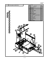
FO-4400U
FO-CS1
5 – 5
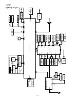
Fig. 3 LC272D0BT-WA6 BLOCK DIAGRAM
4) LC272D0BT-WA6 (IC6): pin-216, QFP (MAIN ASIC)
The device is the embed-array, which has the following functions.
1
CPU interface
The block has the following functions.
That is, mapping executed in memory areas CS0 and CS4, that are
generated by main CPU (SH-3), and then wait control and access
control to the peripheral devices.
2
NOR type flash memory interface
The block has control the protections to each block of a NOR flash
memory. The NOR flash memory is used as two provided blocks;
programming memory block and the entry and history data block.
3
NAND type flash memory interface
The block has the following functions. That is, access control to flash
memory (standard setting memory and optional setting memory), and
generates ECC code at accessing NAND flash memory.
4
DMA request control
The block has the following functions. That is, generate the two inter-
nal DMA requests; read request from FIFO buffer for encodes and
write request from FIFO buffer for decodes. And set each request to
the DMA request channels, ch0 and ch1 by setting register.
5
Interrupt request control
The block has the following functions. That is, encode interrupt re-
quest signal code by each generated interrupt priority level. And then
at the each interrupt, set priority level, mask and clear interrupt fac-
tor.
6
CIS control and image processing
The block has the following functions. That is control the CIS and A/
D converts the scanning image data from analogue to digital, and
executes the converted image data processing.
7
Print image processing and output printing data
The block has the following functions. That is, converts the image
data for printing into 400dpi, and applies smoothing processing. And
then, output the printing data, according to /HSYNC signal from PCU.
8
CODEC
The block has the following functions. The One, the encoding from
the image data (bit map data) in the page memory to the code data
(MMR/MH) in the system memory. The other, the decoding from the
code data (MMR/MH) in system memory to the image data (bit map
data) in the page memory.
9
Page memory (SDRAM) interface
SDRAM is used as Page memory. The block has the controller of
SDRAM and the arbiter of the accesses to SDRAM.
F
Scanner motor control
The block has the following function. That is, controls the PWM cur-
rent control type stepping motor driver that uses a bipolar drive
scheme.
G
Panel/LCD control
The block has I/O port for key sense and LCD control.
CLOCK DIVIDER BLOCK
CPU INTERFACE
DMA REQUEST
CONTROL BLOCK
RUN-LENGTH DECODE
FIFO(CH0)BLOCK
RUN-LENGTH DECODE
FIFO(CH0)BLOCK
RUN-LENGTH DECODE
FIFO(CH1)BLOCK
RUN-LENGTH ENCODE
FIFO(CH1)BLOCK
JBIG CODEC
(CH1)
JBIG CODEC
(CH0)
SCANNER MOTOR
CONTROL BLOCK
PANEL/LCD
CONTROL BLOCK
BUS INTERFACE
(BUS OR CIRCUIT)
INTERRUPT REQUEST
CONTROL BLOCK
PRINTING DATA
PROCESSING BLOCK
MMR/MH FIFO
BLOCK
AT DECODE MODE
MMR/MH FIFO
BLOCK
AT ENCODE MODE
MMR/MH CODEC
PRINTING IMAGE
DATA PROCESSING
BLOCK
S/P CONVERSION
& FIFO BLOCK
SCANNING IMAGE
DATA PROCESSING
BLOCK(INCLUDE ADC)
REQ
REQ
REQ
ARBITER
SDRAM
CONTROLLER
DREQ
IREQ
Содержание FO 4400 - B/W Laser - All-in-One
Страница 125: ...FO 4400U FO CS1 Control PWB parts layout Top side 6 16 ...
Страница 126: ...FO 4400U FO CS1 Control PWB parts layout Bottom side 6 17 ...
Страница 128: ...FO 4400U FO CS1 LIU PWB parts layout Top side 6 19 ...
Страница 129: ...FO 4400U FO CS1 LIU PWB parts layout Bottom side 6 20 ...
Страница 132: ...FO 4400U FO CS1 Printer PWB parts layout Top side 6 23 ...
Страница 133: ...FO 4400U FO CS1 Printer PWB parts layout Bottom side 6 24 ...
Страница 135: ...FO 4400U FO CS1 Power Supply PWB parts layout 6 26 The Power supply PWB of this model employs lead free solder ...
Страница 143: ...FO 4400U FO CS1 M E M O 6 34 ...


