background image

FO-4400U

FO-CS1

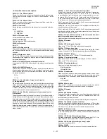
[4] Error code table

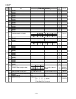
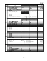
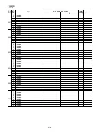
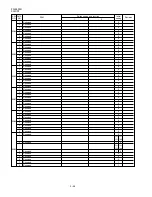
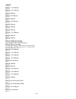
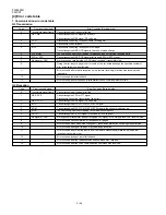
1. Communication error code table

G3 Transmission

G3 Reception

2 – 36

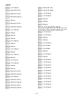
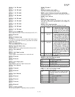
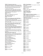
Code

Final received signal

Error Condition (Receiver side)

0

Incomplete signal frame

Cannot recognize bit stream after flag

1

NSF, DIS

Cannot recognize DCS signal by echo etc.

Cannot recognize NSS signal (FIF code etc)

2

CFR

Disconnects line during reception (carrier missing etc)

3

FTT

Disconnects line by fallback

4

MCF

Disconnects line during reception of multi page

Cannot recognize NSS, DCS signal in the case of mode change

5

PIP or PIN

The line is hung up without replying to telephone request from the receiving party.

6

RTN or RTP

Cannot recognize NSS, DCS signal after transmit RTN or RTP signal.

7

No signal or DCN

No response on receiver side or DCN signal received* (transmitter side)

8

Owing to error in some page the error could not be corrected although the specified number of

error retransmission was attempted.

11

Error occurred after or while reception by the remote (receiving) machine was revealed to be

impossible.

12

Error occurred just after fallback.

13

Error occurred after a response to retransmission end command was received.

Code

Final received signal

Error Condition (Receiver side)

0

Incomplete signal frame

Cannot recognize bit stream after flag

1

NSS, DCS

Cannot recognize CFR or FTT signal

Disconnects line during transmission (line error)

2

NSC, DTC

Cannot recognize NSS signal (FIF code etc)

3

EOP

Cannot recognize MCF, PIP, PIN, RTN, RTP signal

4

EOM

Cannot recognize MCF, PIP, PIN, RTN, RTP signal in the case of mode change

5

MPS

The line is hung up without replying to communication request.

6

PR1-Q

Cannot recognize PIP, PIN signal in the case of TALK request

7

No signal or DCN

No response in transmitter (cannot recognize DIS signal) or DCN signal received* (receiver side)

8

Error occurred upon completion of reception of all pages.

9

Error occurred when mode was changed or Transmission/Reception switching was performed.

10

Error occurred during partial page or physical page reception.

11

Error occurred after or during inquiry from the remote (transmitting) machine as to whether

reception is possible or not.

12

Error occurred during or just after fallback.

13

Error occurred after the retransmission end command was received.

14

Error occurred after the voice communication command was received.

Содержание FO 4400 - B/W Laser - All-in-One

Страница 1: ...focusing of the laser beam is achieved on the eyes retina there is danger of spot damage to the retina The following cautions must be observed to avoid exposure of the laser beam to your eyes at the time of servicing 1 When a problem in the laser optical unit has occurred the whole optical unit must be exchanged as a unit not an individual part 2 Do not look into the machine with the main switch t...

Страница 2: ...ll the verification stamp FO 45VS 3 33 CHAPTER 4 DIAGRAMS 1 Block diagram 4 1 2 Wiring diagram 4 2 3 Point to point diagram and connector signal name 4 3 CHAPTER 5 CIRCUIT DESCRIPTION 1 Circuit description 5 1 2 Circuit description of control PWB 5 1 3 Circuit description of CIS unit 5 15 4 Circuit description of LIU PWB 5 16 5 Circuit description of operation panel PWB 5 18 6 Circuit description ...

Страница 3: ...ng lead free solder The Power supply PWB of this model employs lead free solder This is indicated by the LF symbol printed on the PWB and in the service manual The suffix letter indicates the alloy type of the solder Example Indicates lead free solder of tin silver and copper 2 2 2 2 2Using lead free solder When repairing a PWB with the LF symbol only lead free solder should be used Using normal t...

Страница 4: ...telephone network Compatibility ITU T CCITT G3 mode Super G3 mode Printing resolution Horizontal 406 lines inch 16 lines mm Vertical 391 lines inch 15 4 lines mm Input document size Automatic feeding Width 5 8 to 10 1 148 to 256mm Length 5 0 to 14 3 128 to 364 mm Manual feeding Width 5 8 to 11 0 148 to 279 mm Length 5 0 to 19 0 128 to 483 mm Effective scanning width 8 2 208 mm max Effective printi...

Страница 5: ...ress this key to dial a Speed Dial number MENU key Press this key to select special functions and settings UP and DOWN arrow keys Volume setting Press these keys to change the speaker volume when the SPEAKER key has been pressed or the ringer volume at any other time COPY HELP key When a document is in the feeder press this key to make a copy of a document At any other time press this key to print...

Страница 6: ...al feed NOTES If you need to send or copy more 50 pages place the ad ditional pages and carefully in the feeder just before the last page is scanned Do not try to force them in as this may cause double feeding or jamming If your document consists of several large or thick pages which must be loaded one at a time insert each page into the feeder as the previous page is being scanned Insert gently t...

Страница 7: ...ed 3 prong AC outlet Important The fax machine requires its own dedicated power outlet The power outlet must not be shared with any other devices In particu lar do not use an extension cord to connect multiple devices to the outlet Note If your area experiences a high incidence of lightning or power surges we recommend that you install surge protectors for the power and telephone lines Surge prote...

Страница 8: ...tridge but not the toner cartridge remove the toner cartridge and place it on a sheet of paper To make the cartridge more compact for disposal press the buttons on the ends of the handle and fold the handle down 3If you are replacing the drum cartridge remove the old cartridge and dispose of it according to local regulations 4Remove the new drum cartridge from its packaging Insert the drum cartrid...

Страница 9: ...e ma chine and shaking it This may increase the number of pages that can be printed before the toner runs out GWhen to replace the drum cartridge When the drum cartridge nears the end of its life the ALARM indica tor on the operation panel will blink and DRUM LIFE REACHED will appear in the display this message appears when approximately 1000 pages can still be printed Use the following replacemen...

Страница 10: ...u find it difficult to load the paper remove the cassette from the machine Pull the cassette out as far as it will go grasp the left side of the cassette with your left hand and then lift it up and out with both hands 5Push the cassette back into the machine making sure it clicks into place 5 Clearing paper jams Clearing a jammed document If the original document doesn t feed properly during trans...

Страница 11: ...the printing paper jams PAPER JAM will appear in the display Follow the steps below to clear the jam 1Press the green release and open the print compartment cover Caution The fusing unit inside the print compartment becomes very hot during operation Be careful not to touch the inside of the compartment 6Replace the toner cartridge and then close the print compartment cover GREEN BLUE 7If you have ...

Страница 12: ...e from the paper cassette 5Place the machine on top of the cassette 1 Insert the cable guide into the cut out in the edge of the metal plate and then fold it in half and hook the top and bottom edges together 2 Insert the 15pin cable through the ferrite core and then connect the cable to the connectors on the machine and the cassette as shown Position the ferrite core in the gap between the bottom...

Страница 13: ...A A P P GAttach the support plate to the left side of the machine inserting the top edges of the plate under the machine housing Make sure that the guides fit into the holes as shown Secure the plate with screws as shown Use 6 mm screws for the holes marked with A and 10 mm screws for the holes marked with P Secure the screws in the order indicated by the numbers Note that the top hole on the righ...

Страница 14: ...ART ENTER to com plete entry if only one digit is entered Enter a full number and press START ENTER 3 When finished press START ENTER 4 Press RESOLUTION or CONTRAST if needed 5 Press START ENTER Rapid Key Dialing 1 Press the desired Rapid Key Speed Dialing 1 Press SPEED DIAL and enter the desired Speed Dial number press START ENTER if you entered a 1 digit number 2 Press START ENTER Direct Keypad ...

Страница 15: ...t IC s from an overcurrent generated in the CIS unit If F1 or F2 are open replace it with a new one 2 F5 ICP S1 0 is installed in order to protect IC s from an overcurrent generated in the panel PWB unit If F5 is open replace it with a new one 3 F100 ICP S1 0 is installed in order to protect IC s from an overcurrent generated in the verification stamp drive circuit If F100 is open replace it with ...

Страница 16: ...CK PATTERN 2 START 04 CHECK PATTERN 3 START 05 CHECK PATTERN 4 START 06 PAPER FEED AGING 1 START 07 PAPER FEED AGING 2 START START 08 BIAS ADJUST MODE2 START 09 LIFE SET MODE START START Then press the key Select the desired item with the key and the key or select with the rapid key Enter the mode with the key START 10 LIFE ALL CLEAR START 11 LIFE ENTRY MODE PCU ROM Ver START 12 LIFE CLEAR MODE ME...

Страница 17: ...ey It is shifted to set the last soft switch with the key It is shifted to set another soft switch by inputting two digits as the switch number When 2 digits are completely input Output of the soft switch list is started 6Inhibition of data change This is also applicable for the optional setting In the following case it is inhibited to change the data with the key error buzzer Switching ON OFF of ...

Страница 18: ...ystem is adjusted By pressing down the START key the document reading lamp 100 ON is turned ON H Product check This is a dialog used in the production process and a mode to execute a specific mode in the series of the flow After the mode end the rest result as to the checked items is printed After moving to the mode the following actions are sequentially ex ecuted 1Memory clear Same as Diagnosis K...

Страница 19: ...r this mode is activated press the START key and the signals will be sent in the following sequence It can be used to check the modem 1 No signal 2 33600BPS V 34 3 31200BPS V 34 4 28800BPS V 34 5 26400BPS V 34 6 24000BPS V 34 7 21600BPS V 34 8 19200BPS V 34 9 16800BPS V 34 10 14400BPS V 34 11 12000BPS V 34 12 9600BPS V 34 13 7200BPS V 34 14 4800BPS V 34 15 2400BPS V 34 16 0 300BPS V 34 17 ANSam Q ...

Страница 20: ... mode is completely all the same as in the ordinary dial mode T Copy diag mode This mode is for automatic mode selection of copy to reduce the time for treatment at the time of production 1 Set 2 sheets of document No problem if there are 2 sheets or more 23 sheet continuous copy 1st sheet in the FINE AUTO 2nd sheet and after that are copied in the H TONE DARK NOTE Input of the image quality and t...

Страница 21: ...entering this mode and selecting the paper feeding aging mode each mode is executed by inputting the number of the above each mode with the numeric number keys and then inputting the print interval with the numeric number keys Refer to the paper feeding aging mode 1 for each mode Each mode stops the action only when the STOP key is pressed by an operator or when an error for print impossible occur...

Страница 22: ...tent in the memory on the control PWB is broken be cause of PWB repair etc In the production stage it is neces sary to execute this in the last process L I F E 1 0 0 0 0 L I F E 2 0 0 0 0 L I F E 3 0 0 0 0 0 0 0 key key 0 0 0 Rapid key 12 Life clear mode The mode is used to respectively clear the life counter of the printer and the counter of the auto feeder For setting proceed with the following ...

Страница 23: ... 0 0 0 S F T S W 1 1 0 0 0 0 0 0 0 S F T S W 1 1 0 0 0 0 0 0 0 S F T S W 1 1 0 0 0 0 0 0 0 S F T S W 2 0 0 0 0 0 0 0 0 S F T S W 99 0 0 0 0 0 0 0 0 Press key during setting To finish the settings halfway between SW1 and SW99 press the STOP key In this case the setting being done to the SW No on display will be nullified while settings done to the preceding SW No remain in effect The soft switch mo...

Страница 24: ... for auto receive is set to 1 time 1 5 Switch to auto receive from manual receive Binary input 8 4 2 1 0 OPTION 6 0 No switch No 5 6 7 8 Data No 0 Set to 0 9 7 EX 0 0 0 0 0 8 eg Switch to auto receive is set to disable 0 Communication results printout Printed at Printed at Printed at Not printed Printed OPTION error only error timer transmis every time memory sion mode only only 1 No 1 0 0 0 1 1 0...

Страница 25: ...Off 1 6 Protocol monitor On Off 0 7 Line monitor On Off 0 8 Reserved 0 Compromised equalizer 0Km 1 8Km 3 6Km 7 2Km Valid when 1 No 1 0 0 1 1 0 transmitting 2 No 2 0 1 0 1 0 3 H2 mode No Yes 0 Signal transmission level Binary input 16 8 4 2 1 For For No 4 5 6 7 8 Data No U S A Canada SW8 4 EX 0 1 1 0 1 For U S A 0 0 5 EX 0 1 0 0 0 For Canada 1 1 6 eg Signal transmission level is set to 10dBm 1 0 7 ...

Страница 26: ...ication speed 2400bps 1200bps 0 EOL detection timer 13sec 25sec 5sec 5sec 4 No 4 0 0 1 1 0 SW12 5 No 5 0 1 0 1 0 Processing of DIS reception after DIS Command A line is Apply to T 30 α transmission retransmitting cut T 30 6 No 6 0 0 1 1 0 7 No 7 0 1 0 1 0 8 The change to DB from DP by Yes No 0 DTMF output level High Binary input 16 8 4 2 1 For For No 1 2 3 4 5 Data No n x 0 5dBm U S A Canada 1 EX ...

Страница 27: ... 0 0 1 1 0 0 0 7 No 7 0 0 0 0 0 1 1 0 8 No 8 0 1 0 0 0 0 0 0 1 Reserved 0 2 Reserved 0 3 Reserved 0 SW17 4 Reserved 0 5 Reserved 0 6 Reserved 0 7 Reserved 0 8 Reserved 1 1 Reserved 1 2 Reserved 0 3 Reserved 0 SW18 4 Reserved 0 5 Reserved 1 6 Reserved 1 7 Reserved 0 8 Reserved 0 1 Reserved 1 2 Reserved 0 3 Reserved 0 SW19 4 Reserved 0 5 Reserved 1 6 Reserved 0 7 Reserved 0 8 Reserved 0 1 Reserved 0...

Страница 28: ...eserved 1 5 Reserved 0 6 Reserved 0 7 Reserved 1 8 Reserved 0 1 Reserved 0 2 Reserved 1 3 Reserved 0 SW24 4 Reserved 0 5 Reserved 1 6 Reserved 1 7 Reserved 0 8 Reserved 0 1 Reserved 0 2 Reserved 0 3 Reserved 0 SW25 4 Reserved 1 5 Reserved 0 6 Reserved 0 7 Reserved 0 8 Reserved 0 1 Reserved 0 2 Reserved 0 3 Reserved 1 SW26 4 Reserved 1 5 Reserved 0 6 Reserved 0 7 Reserved 1 8 Reserved 0 1 Reserved ...

Страница 29: ... A Canada 4 Reserved 0 0 5 Reserved 1 1 6 Reserved 1 0 7 Reserved 0 0 8 Reserved 1 0 1 Reserved 0 2 Reserved 0 3 Reserved 0 SW31 4 Reserved 0 5 Reserved 0 6 Reserved 0 7 Reserved 0 8 Reserved 0 1 Reserved 1 2 Reserved 0 3 Reserved 1 SW32 4 Reserved 0 5 Reserved 0 6 Reserved 0 7 Reserved 1 8 Reserved 0 1 Reserved 1 2 Reserved 1 3 Reserved 1 SW33 4 Reserved 0 5 Reserved 1 6 Reserved 1 7 Reserved 1 8...

Страница 30: ...served 0 1 SW36 3 Reserved 0 1 4 Reserved 0 0 5 Reserved 0 0 6 Reserved 0 7 Reserved 0 8 Reserved 0 1 Reserved 0 2 Reserved 0 3 Reserved 0 SW37 4 Reserved 0 5 Reserved 0 6 Reserved 1 7 Reserved 0 8 Reserved 1 1 Reserved 0 2 Reserved 0 3 Reserved 0 SW38 4 Reserved 0 5 Reserved 0 6 Reserved 0 7 Reserved 0 8 Reserved 0 1 Reserved 0 2 Reserved 0 3 Reserved 0 SW39 4 Reserved 0 5 Reserved 0 6 Reserved 0...

Страница 31: ...d 0 SW42 4 Reserved 0 5 Reserved 0 6 Reserved 0 7 Reserved 0 8 Reserved 0 1 Reserved 0 2 Reserved 0 3 Reserved 0 SW43 4 Reserved 0 5 Reserved 0 6 Reserved 0 7 Reserved 0 8 Reserved 0 1 Reserved 0 2 Reserved 0 3 Reserved 0 SW44 4 Reserved 0 5 Reserved 0 6 Reserved 0 7 Reserved 0 8 Reserved 0 1 Reserved 0 2 Reserved 0 3 Reserved 0 SW45 4 Reserved 0 5 Reserved 0 6 Reserved 0 7 Reserved 0 8 Reserved 0...

Страница 32: ... 6 Reserved 0 7 Reserved 0 8 Reserved 0 1 Reserved 0 2 Reserved 0 3 Reserved 0 SW48 4 Reserved 0 5 Reserved 0 6 Reserved 0 7 Reserved 0 8 Reserved 0 1 Reserved 0 2 Reserved 0 3 Reserved 0 SW49 4 Reserved 0 5 Reserved 0 6 Reserved 0 7 Reserved 0 8 Reserved 0 1 Reserved 0 2 Reserved 0 3 Reserved 0 SW50 4 Reserved 0 5 Reserved 0 6 Reserved 0 7 Reserved 0 8 Reserved 0 1 Reserved 0 2 Reserved 0 3 Reser...

Страница 33: ... 2 Reserved 0 3 Reserved 0 SW54 4 Reserved 0 5 Reserved 0 6 Reserved 0 7 Reserved 0 8 Reserved 0 1 Reserved 0 2 Reserved 0 3 Reserved 0 SW55 4 Reserved 0 5 Reserved 0 6 Reserved 0 7 Reserved 0 8 Reserved 0 1 Reserved 0 2 Reserved 0 3 Reserved 0 SW56 4 Reserved 0 5 Reserved 0 6 Reserved 0 7 Reserved 0 8 Reserved 0 1 Reserved 0 2 Reserved 0 3 Reserved 0 SW57 4 Reserved 0 5 Reserved 0 6 Reserved 0 7 ...

Страница 34: ...On Off 0 2 Reserved 0 3 Verification stamp Yes No 0 4 Day light saving No Yes 1 SW61 Key buzzer volume Off High Low Low 5 No 5 0 0 1 1 1 6 No 6 0 1 0 1 0 7 Reserved 0 8 Reserved 0 High High Middle Low 1 Speaker volume No 1 0 0 1 1 1 2 No 2 0 1 0 1 1 3 Reserved 1 SW62 4 Reserved 0 Off High Middle Low 5 Ringer volume No 5 0 0 1 1 1 6 No 6 0 1 0 1 1 7 Reserved 0 8 Reserved 0 1 Reserved 0 2 Reserved 1...

Страница 35: ...0 0 1 1 Combination 0 3 No 3 0 1 0 1 1 SW66 Cassette selection of separate page None Tray 1st Cass 2nd Cass OPTION 4 No 4 0 0 1 1 0 5 No 5 0 1 0 1 1 6 Reserved 0 7 Reserved 0 8 Reserved 0 Power save mode OFF ON OPTION 1 No 1 0 0 0 2 No 2 0 1 0 Density adjustment of print bias Binary input 4 2 1 set to 1 7 SW67 3 No 3 4 5 Data No 1 faint 6 deep 1 set to 0 is 4 EX 1 0 0 0 equal to 4 5 eg Bias is set...

Страница 36: ...ed 0 7 Reserved 0 8 Reserved 0 1 Reserved 0 2 Reserved 0 3 Reserved 0 4 Reserved 0 SW73 5 Reserved 0 Data reduction AUTO 100 The number in is 6 Except notation Setting prohibition No 6 0 1 Set up to 100 except the 0 applicable for the 7 No 7 0 0 notation 0 footer print on Auto 8 No 8 0 0 0 is equivalent to 100 1 Automatic printing of activity report Yes When memory full No First data is cleared wh...

Страница 37: ...LTR A4 Tray A4 LTR 0 2 Cassette define LTR A4 Upper A4 LTR 0 When W cassette 3 Cassette define LTR A4 Lower A4 LTR 0 IgnorewhenWcassette 4 Reserved 1 SW77 5 Reserved 1 6 Reserved 0 7 Reserved 0 8 Reserved 0 1 Reserved 1 2 Reserved 0 3 Reserved 0 SW78 4 Reserved 0 5 Reserved 0 6 Reserved 0 7 Reserved 0 8 Reserved 0 1 Secure billing code Yes No 0 2 Pause with SHIFT key Yes No 0 Only when special bil...

Страница 38: ...W83 4 Reserved 0 5 Reserved 0 6 Reserved 1 7 Reserved 0 8 Reserved 1 1 Reserved 0 2 Reserved 0 3 Reserved 0 SW84 4 Reserved 0 5 Reserved 0 6 Reserved 0 7 Reserved 0 8 Reserved 0 1 Reserved 0 2 Reserved 0 3 Reserved 0 SW85 4 Reserved 0 5 Reserved 1 6 Reserved 0 7 Reserved 1 8 Reserved 0 1 Reserved 0 2 Reserved 0 3 Reserved 0 SW86 4 Reserved 0 5 Reserved 0 6 Reserved 0 7 Reserved 0 8 Reserved 0 SW N...

Страница 39: ...d 1 SW90 4 Reserved 0 5 Reserved 0 6 Reserved 1 7 Reserved 0 8 Reserved 1 1 Reserved 0 2 Reserved 0 3 Reserved 0 SW91 4 Reserved 0 5 Reserved 0 6 Reserved 0 7 Reserved 0 8 Reserved 0 1 Reserved 0 2 Reserved 1 3 Waiting time after dialing 90sec The specification of each country is followed 0 SW92 4 Show receiver s name Yes Show No Hide 1 5 Reserved 0 6 Reserved 0 7 Reserved 0 8 Reserved 0 1 Reserve...

Страница 40: ...rved 0 6 Reserved 0 7 Reserved 0 8 Reserved 0 1 Reserved 0 2 Reserved 0 3 Reserved 0 SW97 4 Reserved 0 5 Reserved 0 6 Reserved 0 7 Reserved 0 8 Reserved 0 1 Reserved 0 2 Reserved 0 3 Reserved 0 SW98 4 Reserved 0 5 Reserved 0 6 Reserved 0 7 Reserved 0 8 Reserved 0 1 Reserved 0 For For U S A Canada 2 Reserved 1 0 For For SW99 U S A Canada 3 Reserved 1 0 4 Reserved 0 5 Reserved 0 6 Reserved 0 7 Reser...

Страница 41: ...lt is produced only a communication error is en countered If No 1 was set to 1 No 2 was set to 1 and No 3 was set to 0 the communication result will be produced every time a communica tion is done even if the communication was successful If No 1 was set to 0 No 2 to 1 and No 3 to 0 the communication result will be produced every transmission Setting No 1 to 1 No 2 to 0 and No 3 to 0 will disable t...

Страница 42: ... SW9 No 3 Equalizer freeze This switch is used to perform reception operation by fixing the equal izer control of modem for the line which is always in an unfavorable state and picture cannot be received Usually the control is executed according to the state of line where the equalizer setting is changed always SW9 No 4 Equalizer freeze conditions Setting which specifies SW9 No 3 control only in c...

Страница 43: ...No 7 Reserved Set to 1 SW26 No 8 Reserved Set to 0 SW27 No 1 Reserved Set to 0 SW27 No 2 Reserved Set to 1 SW27 No 3 No 8 Reserved Set to 0 SW28 No 1 No 2 Reserved Set to 0 SW28 No 3 No 5 Reserved Set to 1 SW28 No 6 No 8 Reserved Set to 0 SW29 No 1 No 4 Reserved Set to 0 SW29 No 5 Reserved Set to 1 SW29 No 6 No 8 Reserved Set to 0 2 29 SW17 No 1 No 7 Reserved Set to 0 SW17 No 8 Reserved Set to 1 S...

Страница 44: ... No 1 No 8 Reserved Set to 0 SW47 No 1 No 8 Reserved Set to 0 SW48 No 1 No 8 Reserved Set to 0 SW49 No 1 No 8 Reserved Set to 0 SW50 No 1 No 8 Reserved Set to 0 SW51 No 1 No 8 Reserved Set to 0 2 30 SW30 No 1 No 4 Reserved Set to 0 SW30 No 5 Reserved For U S A Set to 1 SW30 No 6 Reserved For U S A Set to 1 SW30 No 6 Reserved For Canada Set to 0 SW30 No 7 Reserved Set to 0 SW30 No 8 Reserved For U ...

Страница 45: ... interval 0 minute SW64 No 6 No 7 Reserved Set to 0 SW64 No 8 Quick on line function It is selected whether auto dial call is activated in the memory input mode when one document is completely read or when all pages are completely read SW65 No 1 No 2 Cassette selection To set selective modes for detail paper cassettes of the printer 00 Manual 01 Automatic 1 10 Automatic 2 11 Except the above To se...

Страница 46: ...n the copy mode however the fine mode is automatically selected unless the MODE key is manually set to an other mode SW71 No 8 Reserved Set to 0 SW72 No 1 Reserved Set to 1 SW72 No 2 Reserved Set to 0 SW72 No 3 Reserved Set to 1 SW72 No 4 No 8 Reserved Set to 0 SW73 No 1 No 5 Reserved Set to 0 SW73 No 6 No 8 Data reduction Reduction ratio of receiving is set It can be changed even in the optional ...

Страница 47: ...use the function of Weak 0 for general cases SW76 No 8 MTF intensity in half tone mode This allows selection of MTF correction dimness correction in the half tone mode When NO 1 is selected the whole image becomes soft and mild On the contrary however mildness of characters will be re duced Normally set to NO 1 SW77 No 1 Cassette define LTR A4 Tray A4 cassette can be used Set 0 or 1 for all of thr...

Страница 48: ...ions SW92 No 4 Show receiver s name This switch is used to note the receiver s name on the transaction report and activity report When this switch is set to 0 the receiver s dial number is printed on the report SW92 No 5 No 8 Reserved Set to 0 SW93 No 1 No 8 Reserved Set to 0 SW94 No 1 No 8 Reserved Set to 0 SW95 No 1 No 4 Reserved Set to 0 SW95 No 5 No 6 Reserved Set to 1 SW95 No 7 Reserved Set t...

Страница 49: ... problems still exist on the machine use the following format and check the related matters TO ATT Ref No CC ATT Date FM Dept Sign Facsimile communication problem Ref No Date From Mr Fax Tel No Our customer Name Tel No Address Fax No Contact person Model name Other party Name Tel No Address Fax No Contact person Model name Problem mode Line Domestic international Mode G3 Phase A B C D Reception Tr...

Страница 50: ...er fallback 13 Error occurred after a response to retransmission end command was received Code Final received signal Error Condition Receiver side 0 Incomplete signal frame Cannot recognize bit stream after flag 1 NSS DCS Cannot recognize CFR or FTT signal Disconnects line during transmission line error 2 NSC DTC Cannot recognize NSS signal FIF code etc 3 EOP Cannot recognize MCF PIP PIN RTN RTP s...

Страница 51: ...etween the PCU and the control PWB RX DOCUMENT TRAY OFF The document receiving tray is not set properly HIGH VOLTAGE ERROR Abnormality with the high voltage portion HEATER LOW ERROR Heater temperature is too low HEATER HIGH ERROR Heater temperature is too high WARMING UP ERROR Warming up is not done properly CHECK COVER OR DRUM Printer cover may be open or the drum cartridge may not be set properl...

Страница 52: ...e following conditions 1 When a communication error occurred in communication in the Super G3 mode due to page 1 MCF reception failure 2 When a communication error occurred in communication in the Super G3 mode after reception of page 1 MCF 3 When a communication error occurred in retransmission 4 When a communication error occurred in sequential system commu nication The retransmission of this co...

Страница 53: ...e documents 1 Make sure that the documents are of suitable size and thickness and free from creases folds curls wet glue wet ink clips staples and pins 2 Place documents face down in the hopper Adjust the document guides to the document width Align the top edge of documents and gently place them into the hopper The first page under the stack will be taken up by the feed roller to get ready for tra...

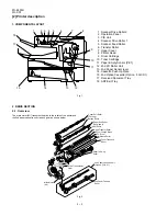
Страница 54: ... lever 14 Cassette Push Up Plate 15 2nd Option Cassette Option FO CS1 17 Received Document Tray 18 ADF Exit Tray 2 DRIVE SECTION 2 1 Overview The main motor M1 transmits the drive to the rollers of the printer and the 2nd paper cassette unit via each gear as shown below Backup Roller Heat Roller Drum Charge Brush Image Transfer Roller Sleeve Roller PC Drum Toner Transport Roller Paper Take up Roll...

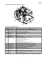
Страница 55: ...rged voltage Developing Sleeve Roller Developing bias voltage Developing Toner Regulation Plate Developing blade voltage Developing Toner Collecting Plate Developing Lower Seal voltage Image Transfer Roller Image transfer voltage PE1 Paper Empty Sensor Detects that a sheet of paper is taken up The signal is L when paper is detected PS1 Paper Take Up Sensor Detects that a sheet of paper is taken up...

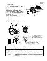
Страница 56: ...d it is determined whether the actual length matches the paper length specified by the controller Fig 6 Print Head Unit Exposure Print Exit Image Transfer Fusing PC Drum Development Drum Cartridge Toner Cartridge 2nd Option Cassette Unit Paper Take up Sensor PS1 Paper Take up Roller Depressing Cam Paper Empty Sensor PE1 Paper Tray Paper Take up Solenoid SL1 Paper Take up Gear 1 3 2 4 Drum Cartridg...

Страница 57: ...face approx 50V Reflector Mirror Print Head Unit PWB D 9 DEVELOPMENT 9 1 Overview Toner is applied to the invisible static image on the PC Drum and a toner image developed image is created on the drum surface VBL VB VSS 6 4 3 8 7 Toner Cartridge 1 2 6 3 4 5 7 8 Developing Lower Seal Voltage terminal VSS Developing Voltage terminal VB Developing Blade Voltage terminal VBL VSS DC 300V DC 400 V max V...

Страница 58: ...ing temperature When the Heater Lamp H1 is not turned OFF even if the Thermistor TH1 detects a high temperature malfunction if the surface temperature of the Heat Roller exceeds 230 C the signal from IC4 79 changes from L to H to turn OFF the Heater Lamp H1 forcibly 1 2 1 2 CN2 2 1 TH1 1 2 CN2 H1 TS1 DC5V 78 IC4 3 2 1 Q103 GND DC5V IC3 79 55 CMPOUT P01 CMPIN AN8 P63 GND GND H1 ON H1 OFF L H H L L ...

Страница 59: ... a sheet of paper etc Sends the vertical direction synchronizing signal when the Paper Take Up Sensor is ON Sends the main scanning direction synchronizing signal Prints out video data for one scan Printing is completed Initiates the printing command Receives the vertical direction synchronizing signal Receives the main scanning direction syn chronizing signal Sends video data for one scan Has one...

Страница 60: ...ON OFF ON Printing Command PRINT Polygon Motor M3 Paper Take Up Sensor PS1 Drum Charge Exposure output Development output Image Transfer output Main Motor M1 Paper Take Up Solenoid SL1 OFF OFF OFF OFF OFF OFF ON ON ON ON ON ON ON Polygon Motor M3 Main Motor M1 Drum Charge output Exposure output Development output Image Transfer output Paper Exit Sensor PS3 DC Charge AC Charge OFF Charge ...

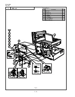
Страница 61: ...isassembly and assembly of such parts and units refer to the Parts List The numbers in the illustration the parts list and the flowchart in a same section are common to each other To assure reliability of the product the disassembly and the assembly procedures should be performed carefully and deliberately 1 Fig 1 Front cabinet Parts list Fig 1 1 2 3 4 1 2 2 4 HOOK 3 HOOK HOOK HOOK HOOK 1 Main uni...

Страница 62: ...FO 4400U FO CS1 3 10 Parts list Fig 2 Fig 2 2 Rear cabinet 1 2 3 4 5 2 3 HOOK 4 5 4 4 4 4 4 HOOK HOOK 1 1 Main unit 1 2 Screw 3 10 1 3 ROM cover 1 4 Screw 3 10 6 5 Rear cabinet 1 No Part name Q ty ...

Страница 63: ...11 Fig 3 Parts list Fig 3 3 PWB plate Right cabinet 1 2 3 4 5 1 2 3 2 2 LIU PWB Printer PWB Control PWB 4 4 5 HOOK HOOK HOOK 1 1 Main unit 1 2 Screw 3 6 6 3 PWB plate 1 4 Screw 3 10 2 5 Right cabinet 1 No Part name Q ty ...

Страница 64: ... 2 2 2 2 5 7 6 Printer PWB Printer PWB Printer PWB Control PWB Control PWB Control PWB LIU PWB 4 4 4 4 4 4 4 7 3 4 PWB unit No Part name Q ty 1 Main unit 1 2 Screw 3 6 7 3 Screw 3 10 1 4 Connector 20 5 LIU PWB unit 1 6 Control PWB unit 1 7 Printer PWB unit 1 ...

Страница 65: ...13 Parts list Fig 5 Fig 5 5 Operation panel unit Upper cover unit 1 2 3 4 5 6 4 1 3 3 5 6 1 2 3 4 3 1 Main unit 1 2 Screw 3 10 1 3 Screw 3 6 6 4 Operation panel unit 1 5 Screw 3 8 1 6 Upper cover unit 1 No Part name Q ty ...

Страница 66: ...7 18 18 17 14 13 16 11 Screw 3 6 1 12 Paper feed tray unit 1 13 Screw 3 10 1 14 Tray width guide front 1 15 Screw 3 10 1 16 Tray width guide rear 1 17 Connector 2 18 Sensor 2 19 Paper feed tray 1 1 Main unit 1 2 Screw 3 6 5 3 Screw 3 10 2 4 Screw 3 6 1 5 Front left frame 1 6 Screw 3 10 2 7 Speaker holder plate spring 1 8 Speaker ass y 1 9 Inner front cabinet 1 10 Screw 3 10 2 No Part name Q ty No ...

Страница 67: ...t Fig 7 Fig 8 8 Inner left cabinet unit Parts list Fig 8 1 2 3 4 5 1 2 4 2 3 5 2 1 Main unit 1 2 Screw 3 8 4 3 Inner left cabinet unit 1 No Part name Q ty 1 2 3 1 2 2 3 2 2 1 Main unit 1 2 Screw 3 6 7 3 Rear left frame 1 4 Screw 3 6 1 5 Bottom left frame 1 No Part name Q ty ...

Страница 68: ...r supply PWB Parts list Fig 9 1 2 3 4 5 6 7 8 1 3 2 2 4 2 2 5 8 7 6 5 5 3 1 Main unit 1 2 Screw 3 6 4 3 Connector 4 4 Power supply PWB unit 1 5 Screw 3 6 3 6 Screw 4 6 1 7 Power supply PWB plate 1 8 Power supply PWB 1 No Part name Q ty ...

Страница 69: ...0 Fig 10 Scanner frame unit 1 2 1 Scanner frame unit 1 2 Screw 3 8 1 3 Operation panel unit 1 4 Screw 3 10 5 5 Screw 3 10 2 6 Document guide upper 1 7 Stopper 1 8 Left upper cabinet 1 No Part name Q ty 1 2 3 4 5 6 7 8 1 3 4 5 6 2 1 8 7 4 5 4 ...

Страница 70: ... CIS cable 1 25 Core 1 26 CIS spring 2 27 Screw 3 6 1 28 FD1 earth spring 1 29 Screw 3 6 1 30 Screw 3 10 1 31 SD2 earth spring 1 32 Verification stamp FO 45VS 1 33 Document sensor switch 1 34 Transfer sensor switch 1 35 Front sensor switch 1 36 Document sensor cable 1 37 Pinch roller spring 2 38 PO pinch roller 2 39 Screw 3 10 2 40 Scanner support plate 1 41 Paper earth brush 1 42 Screw 3 10 2 43 ...

Страница 71: ...ase lever spring 1 6 Screw 3 10 2 7 Document upper plate 1 8 Brush earth spring 1 9 Separate spring 1 10 Pinch roller spring 2 4 11 Pinch roller shaft 2 12 Pinch roller 4 13 Separate plate 1 14 Separate gum 1 15 Separate sheet 1 16 Transfer plate piece 1 17 Input pressure spring 1 18 Back sheet 1 19 Paper brush 1 20 Back guide 1 21 Back bracket 1 22 Document guide upper 1 23 Screw 3x10 1 24 LCD su...

Страница 72: ...xit guide upper 1 17 Pinch roller ass y 2 18 Screw 3 8 1 19 Pinion gear 1 20 Hopper spring 1 21 Upper cover lock button 1 22 Hopper guide left 1 23 Hopper guide right 1 24 Upper cover 1 1 Screw 3 10 5 2 Screw 3 8 2 3 Upper cover lock spring 1 4 Upper cover lock nail 1 5 Drum cartridge detect 1 lever spring 6 Drum cartridge detect lever 1 7 Shutter lever 1 8 Idler gear 32z 5 9 Upper cover roller 1 ...

Страница 73: ...e Motor cable CIS cable CNPW Sensor cable Sensor cable Control PWB Control PWB Printer PWB Printer PWB Speaker cable LIU PWB LIU PWB LIU cable LIU cable CN15 CN12 CN14 CN3 CN9 CN5 2 times CIS cable Rib 3 Scanner frame Front sensor cable Red CIS cable Not used Rib Rib Rib Rib Document sensor cable White Transfer sensor cable Yellow 3 Rib 1 Band 100mm 4 2 Core F2125 1 3 Core F2124 2 4 Band 1 5 Screw...

Страница 74: ...ltage PWB HV1 CN1 CN3 Cooling Fan Motor Fig 15 15 High voltage PWB unit HV1 1 Remove the Cooling Fan Motor 2 screws 2 Remove the 2 covers 9 screws 3 Remove the 2 connectors 4 Remove the High Voltage PWB 2 screws 1 Remove the Paper Take up Sensor PS1 1 connector ...

Страница 75: ... Main motor M1 Fig 16 1 Remove the gear plate 4 screws 2 Remove 2 gears 3 Remove the left side plate 4 screws and 1 connector 5 Remove the cartridge positioning plate Tabs at 4 places 6 Remove the Main Motor Unit M1 4 screws ...

Страница 76: ...ove the Paper Take up Roller 17 Paper take up roller a b c Fig 17 18 Print head unit PH 19 Paper empty sensor PE1 1 Unplug the connector from the Main Motor Unit and remove the harness from the cord holder 2 Unplug the connectors from the cord holder 3 Remove the Print Head Unit PH 6 screws Fig 19 1 Remove the sensor fixing bracket and remove the Paper Empty Sensor 1 connector ...

Страница 77: ...the sensor fixing bracket and the Paper Exit Sensor PS3 3 Remove the Heater Lamp holding cover 1 screw and 1 spring 4 Remove the 2 mounting screws 5 Pressing the right and left tabs at 2 places separate the upper half of the Fusing Unit from the lower half a b c Bushing Backup Roller Fusing Entrance Guide 6 Remove the bushings and the Backup Roller 7 Remove the Fusing Entrance Guide a Push the Fus...

Страница 78: ...r from the Heat Roller 11 Slide the Heat Roller to the right a swing out the left end b and then slide the roller in the direction of c and pull it out NOTE To prevent the surface of the Heat Roller from being scratched by the Fusing Separators lift the separators when removing and reinstalling the roller Use utmost care not to damage the surface of the roller 12 Remove the Fusing Paper Separators...

Страница 79: ...CS1 3 27 Fig 22 22 Paper cassette FO CS1 Parts list Fig 22 3 3 3 5 4 6 1 2 3 4 5 2 2 2 1 3 1 6 1 Paper cassette ass y 1 2 Screw 3 10 3 3 Screw 3 10 4 4 Screw 3 6 1 5 Screw 3 12 1 6 Bottom plate 1 No Part name Q ty ...

Страница 80: ...assette PWB unit FO CS1 Fig 23 7 3 4 2 6 6 5 5 5 5 1 1 2 3 4 5 6 7 Hook Parts list Fig 23 1 Cassette cabinet unit 1 2 Cassette case unit 1 3 Paper sensor lever 1 4 Sensor guide plate 1 5 Connector 4 6 Screw 3 10 2 7 Cassette PWB unit 1 No Part name Q ty ...

Страница 81: ...g 24 1 Cassette cabinet unit 1 2 Screw 3 8 1 3 Screw 3 10 1 4 Screw 3 10 1 5 Front support bracket 1 6 Screw 3 10 3 7 Clutch spring 1 8 Paper feed clutch gear 1 9 PU roller bearing 1 10 PU roller unit Cassette up roller shaft 1 11 Drive roller 1 12 Drive roller bearing 1 13 Drive system unit 1 14 Cassette size sensor 1 15 Screw 3x8 2 16 Paper size sensor 1 No Part name Q ty ...

Страница 82: ...arts list Fig 25 1 Cassette cabinet unit 1 2 Screw 3 10 2 3 Cassette paper guide 1 4 Idler gear 1 5 Earth spring 1 6 Lever joint 1 1 7 Pinch roller 2 8 Pinch roller shaft 1 9 Pinch roller spring 2 10 Release lever spring 1 11 Lever joint 2 1 12 Release lever Gear plate 1 13 Release shaft 1 14 Cassette cabinet 1 No Part name Q ty ...

Страница 83: ...ase unit 1 2 Screw 3 10 2 3 Cassette push up plate holder 2 4 Screw 3 10 2 5 Cassette back guide plate 1 6 Cassette back guide 1 7 Cassette push up plate 1 8 Cassette push up plate spring 2 9 Screw Special 2 10 Slide roller 2 11 Screw 3x10 2 12 Lock down spring 2 1 13 Lock down piece 2 1 14 Lock down holder 1 15 Screw 3x8 1 16 Lock down spring 1 17 Lock down piece 1 1 No Part name Q ty ...

Страница 84: ... case 2 2 FO CS1 Fig 27 4 4 4 4 3 5 1 2 2 2 2 1 2 3 4 5 Parts list Fig 27 1 Cassette case unit 1 2 Screw 3 10 4 3 Cassette width guide separate nail front 1 4 Screw 3 10 4 5 Cassette width guide separate nail rear 1 No Part name Q ty ...

Страница 85: ...move the screws B1 x 5 pcs to remove document guide under 4 Remove CIS unit Carefully bend 2 hooks and remove CIS cable 5 Install the verification stamp FO 45VS with the screw B2 x 1pc Operation panel unit Document guide stopper Screw A1 x 1 Open Hook Hook Scanner frame unit Stamp cable to Control PWB Document guide under Screw B1 x 5 Screw B2 x 1 CIS cable CIS unit FO 45VS ...

Страница 86: ...the verification stamp FO 45VS set the soft SW 27 No 3 initial setting to 1 8 Replacing the verification stamp If you are using the Verification Stamp function you will need to replace the ink cartridge in the stamp unit when it runs out of ink when the stamped mark on original documents becomes faint A new ink cartridge can be obtained from your dealer 1Remove the original document OUT tray Fig 1...

Страница 87: ...o 400dpi B4 SDRAM 8MB 8 3 30ppm Option FO 8MK based on LC821033 A4 CIS Memory PWB Image Memory 8 Run length Converter 203dpi 8pixel mm Image Memory NAND Flash 8MB Panel Controller NAND Flash 8 Motor Controller Scan Mechanism 8MB CPU I F Mapper Stepping Motor GPIO port serial RTC Backup Print Data Processor SM8578BV LIU PWB MODEM Line1 8 ECC Code Generator HSYNC TOD etc Printer PWB MINOLTA NC L601 ...

Страница 88: ...R PRINTER PWB PE1 PAPER EMPTY SENSOR 8 5 6 2 2 TEL LINE LIU PWB CNLIU1 10 3 3 2 5 POWER SUPPLY PWB 4 1 2 1 1 12 8 2 30 2 30 2 4 10 9 2 TRANSFER SENSOR FRONT SENSOR DOCUMENT SENSOR 2 2 2 8 CN1 CN7 CN14 CN2 CN10 CN15 CN4 CN6 CN13 CN11 CN12 CN3 CN8 CN5 CN9 4 28 LED PWB 15 COG LCD 20x2 Characters 14 14 CNCOGA JOINT PWB CNCOGB CNLEDA CNCOG OPERATION PANEL PWB CNPNA TX MOTOR PS4 PAPER OUT SENSOR 2 3 OPT...

Страница 89: ...R LOW LD EN SH N GND DG L DATA 5V SOS 5V LD POWER LOW LD EN SH N GND DG L DATA 5V HV1 HIGH VOLTAGE PWB UNIT CN4 CN1 CN1 1 2 3 4 5 6 7 8 9 10 10 9 8 7 6 5 4 3 2 1 5V CH LREM T VR T MON V T MON I B VR C REM C MON GND MG 24V 5V CH LREM T VR T MON V T MON I B VR C REM C MON GND MG 24V SL1 PAPER TAKE UP SOLENOID 2ND PAPER CASSETTE PWB CN11 1 2 3 4 5 6 7 8 9 10 11 12 13 14 15 1 2 3 4 5 6 7 8 9 10 11 12 ...

Страница 90: ...NANDRD DEN OPD7 OPD6 OPD5 OPD4 OPD3 OPD2 OPD1 OPD0 MEMDTC0 DG MEMDTC1 DG DG DG DG DG CLEO DG ALEO DG WP1 3 3V NANDWR 3 3V OPCS 3 3V BUSYOP R W NANDRD DEN OPD7 OPD6 OPD5 OPD4 OPD3 OPD2 OPD1 OPD0 MEMDTC0 DG MEMDTC1 DG DG DG DG 1 2 3 4 5 6 7 8 9 10 11 12 13 14 15 16 17 18 19 20 21 22 23 24 25 26 27 28 29 30 1 2 3 4 5 6 7 8 9 10 11 12 13 14 15 16 17 18 19 20 21 22 23 24 25 26 27 28 29 30 CNOP1 CONTROL...

Страница 91: ...2 Mbit FLASH MEMORY This is a flash memory writing program and is also used for the registra tion data such as telephone directory 32 Mbit area is divided into 2 for every 16 Mbit the lower order and higher order address sides are used for the program and for the regis tration data respectively 3 W986416DH or MT48LC4M16A2TG IC25 pin 54 TSOP 64 Mbit SDRAM The program stored in the flash memory IC12...

Страница 92: ...mer Clock pulse generator watchdog timer Central processing unit D A converter DMAC H UDI INTC MMU RTC SCI SCIF TLB TMU UBC Direct memory access controller Hitachi user debugging interface Interrupt controller Memory management unit Realtime clock Serial communication interface with smart card interface Serial communication interface with FIFO Address translation buffer Timer unit User break contr...

Страница 93: ...on 52 O A5 Address bus 53 O A6 Address bus 54 O A7 Address bus 55 O A8 Address bus 56 O A9 Address bus 57 O A10 Address bus 58 O A11 Address bus 59 O A12 Address bus 60 O A13 Address bus 61 VssQ Input output power supply 0 V 62 O A14 Address bus 63 VccQ Input output power supply 3 3 V 64 O A15 Address bus 65 O A16 Address bus 66 O A17 Address bus 67 O A18 Address bus 68 O A19 Address bus 69 O A20 ...

Страница 94: ...4 SCIF transmit request 2 SC port 145 I RxD0 SCPT 0 SCI receive data 0 SC port 146 I RxD2 SCPT 2 SCIF receive data 2 SC port 147 I CTS2 IRQ5 SCPT 5 SCIF transmit clear external interruption request SC port 148 Vss Internal power supply 0 V 149 I RESETM Manual reset request 150 Vcc Internal power supply 1 9 V 151 I I I O IRQ0 IRL0 PTH 0 External interrupt request input output port H 152 I I I O IRQ...

Страница 95: ...S and A D converts the scanning image data from analogue to digital and executes the converted image data processing 7Print image processing and output printing data The block has the following functions That is converts the image data for printing into 400dpi and applies smoothing processing And then output the printing data according to HSYNC signal from PCU 8CODEC The block has the following fu...

Страница 96: ...VSS Ground 29 O XRDOUT 83 O SDCLK Clock of page memory 30 O XWAIT Wait request signal 84 O DQMUL Data mask of page memory 31 I XBUSYDP Busy signal of Dual port RAM 85 CKE CK enable of page memory 32 I XMDMINT1 86 O CASB CAS of page memory 33 I XMDMINT0 87 O RASB RAS of page memory 34 O XMDMCS1 Chip select Modem Chip 1 88 DWEB Write strobe of page memory 35 O XMDMCS0 Chip select Modem Chip 0 89 XCS...

Страница 97: ...A22 Address bus bit22 134 I SEN5 Key sense signal 188 I A21 Address bus bit21 135 I SEN4 Key sense signal 189 I A20 Address bus bit20 136 I SEN3 Key sense signal 190 I A13 Address bus bit13 137 I SEN2 Key sense signal 191 I A12 Address bus bit12 138 I SEN1 Key sense signal 192 I A11 Address bus bit11 139 I SEN0 Key sense signal 193 I A10 Address bus bit10 140 B LD15 LED 194 I A9 Address bus bit9 1...

Страница 98: ...tion to RTC the device set and read the time 5Verification stamp control The software control on off of the verification stamp And the control block has hardware timer instead of the continuous stamp on status 6Original sensor detect The software detects the original sensor And then the control block has the generated interrupt circuitry by detecting the sensor signal risen fallen Fig 4 LC24199B W...

Страница 99: ...oard 32 O XNICACKP Acknowledge signal for NIC in PCL mode 86 B DPONIC3 33 I RXWP READ WRITE signal from PCL 8 DPONIC4 34 P VDD Power supply 88 VDD Power supply 35 P VSS Ground 89 P VSS Ground 36 I PCLKPCL Serial communication clock in PCL mode 90 DPONIC5 37 O PSTSPCL Status data from PCU in PCL mode 91 B DPONIC6 38 I PCMDPCL Command data to PCL in PCL mode 92 B DPONIC7 39 O PACK Printing acknowled...

Страница 100: ...NIC board 178 B D4 127 O XCSNICIN 179 B D3 128 I GPIO4 PWSAVE Powr save control for PS unit 180 B D2 129 I GPIO5 LEDON Light ON OFF for LED in CIS 181 B 130 I GPIO6 VPPCN VPP control of nor flash memory 182 B 131 I GPIO7 XWP Write protect for nor flash memory 183 N C Not connect 132 I XNICACK Acknowlede signal for NIC 184 O INTR 133 I XROLSNS Roller position sensor 185 I XRESET 134 I XORGSNS Docum...

Страница 101: ...te Adaptation ARA in V 34 half duplex Auto dial and auto answer control TTL and CMOS compatible DTE interface ITU T V 24 EIA TIA 232 E data control Microprocessor bus data configuration control Receive dynamic range 0 dBm to 43 dBm for V 17 V 33 V 29 V 27 ter and V 21 9 dBm to 43 dBm for V 34 half duplex Caller ID Demodulation Single tone detection in Data Mode ADPCM Voice Mode Conexant Proprietar...

Страница 102: ...2000 TCM3 TCM Note 2 12000 Note 2 Note 2 Note 2 Note 2 V 34 9600 TCM3 TCM Note 2 9600 Note 2 Note 2 Note 2 Note 2 V 34 7200 TCM3 TCM Note 2 7200 Note 2 Note 2 Note 2 Note 2 V 34 4800 TCM3 TCM Note 2 4800 Note 2 Note 2 Note 2 Note 2 V 34 2400 TCM3 TCM Note 2 2400 2400 only Note 2 Note 2 Note 2 V 32 bis 14400 TCM TCM 1800 14400 2400 6 1 128 V 32 bis 12000 TCM TCM 1800 12000 2400 5 1 64 V 32 bis 9600...

Страница 103: ...phone Line Interface 50 PWR VDD FM336Plus IC30 Terminal description PIN I O Name Interface 51 RESERVED NC 52 GND VSUB 53 GND VSS 54 NC NC 55 NC NC 56 MI SLEEP Modem Interconnect 57 PWR VDD1 58 NC NC 59 RESERVED NC 60 RESERVED NC 61 MI SR1IO Modem Interconnect 62 PWR VCORE 63 PWR VDD1 64 IA XTCLK DTE Serial Interface 65 GND VSS 66 RESERVED NC 67 OA RXD DTE Serial Interface 68 IA DTR DTE Serial Inte...

Страница 104: ...he scanner and the page memory for printing This memory is controlled by the MAIN ASIC directly The page memory for scanner is composed of the partial area of IC5 The image data of approx one page except in the super fine mode of the draft read with the scanner can be stored They are stored until they are contracted by CODEC function in MAIN ASIC The page memory for printing is composed of the rem...

Страница 105: ... H input output OFF L input output ON I01 I11 22 23 Digital inputs that set the output current I02 I12 21 20 The output currents can be set to 1 3 2 3 or full by setting these pins to appropriate combinations of high and low levels VCC 28 Logic block power supply LB1845 IC3 Terminal description 3 Circuit description of CIS unit 1 CIS CIS is an image sensor which puts the original paper in close co...

Страница 106: ...urge voltage occurring on the telephone line The AR1 protect the circuit from the 390V or higher line surge voltages The AR2 and AR3 protect the circuit from the 500V or higher verti cal surge voltages The ZD6 and ZD7 control the voltage generated on the secondary side of matching transformer to 2V 2 On hook status detection circuit The on hook status detection circuit detects the Status of the pu...

Страница 107: ...ional amplifier transmits the voice transmission signal to the line and feeds back the voice signal to the voice reception circuit as the side tone 7 Signal selection The following signals are used to control the transmission line of FAX signal For details refer to the signal selector matrix table NO Signal Name CNLIU 1 RXIN 2 TXOUT 3 CI 4 EXHS 5 DPON N C NO Signal Name CNLIU 6 CML 7 5V 8 DG 9 24V...

Страница 108: ...peration panel PWB The operation panel PWB includes the ten key scan circuit and the LED lighting circuit The LS145 is controlled through LD0 LD3 4 bits and ten key detection is performed The HC174 is controlled through LD0 LD5 6 bits to provide LED lighting information 2 COG LCD LMG2025 TPR The COG uses the one chip LCD driver IC to display 20 digits x 2 lines The LCD display density is controlle...

Страница 109: ...ary winding Control of constant voltage is carry out by as follows Feedback put on control circuit through photo coupler from 24 V Out put Over Current Protection Circuit detect spread of ON period by Out put Load is heavy and extend OFF period by control circuit And turn down energy that accumulating in primary winding Over Current Protection is make secondary side of output voltage 24 V s rising...

Страница 110: ...1 1u 6 3V C239 N M TP505 R256 10K C221 N M C22 1u 6 3V C222 R286 N M R293 4 7K C224 TP3 R355 C20 1u 6 3V IC17 PST596 C17 1u 6 3V R352 R302 0 R360 0 R260 0 R294 4 7K C218 TP2 R332 4 7K L101 0 1608 2125 C23 1u 6 3V R454 0 C19 1u 6 3V R357 N M R32 IC15 N M CDC2509CPWR R300 0 C274 R296 10K C217 R257 N M Q110 C241 N M R359 N M R301 10K R3544 7K C248 1u C245 0 1u C25 1u 6 3V C220 0 1u R336 0 C276 C21 1u...

Страница 111: ...0 140 SCK0 SCPT 1 141 TxD2 SCPT 2 142 SCK2 SCPT 3 143 RTS2 SCPT 4 144 RxD0 SCPT 0 145 RxD2 SCPT 2 146 CTS2 IRQ5 SCPT 5 147 IRQ0 IRL0 PTH 0 151 IRQ1 IRL1 PTH 1 152 IRQ2 IRL2 PTH 2 153 IRQ3 IRL3 PTH 3 154 IRQ4 PTH 4 155 DREQ0 PTH 5 160 DREQ1 PTH 6 161 XTAL2 2 EXTAL2 3 ASEMD0 122 XTAL 131 EXTAL 132 MD1 129 MD0 163 MD2 164 RESETM 149 RESETP 165 MD3 167 MD4 168 MD5 169 AN 0 PTJ 0 171 AN 1 PTJ 1 172 AN ...

Страница 112: ...MA3 95 MA2 94 MA1 93 MA0 92 XCSDRM0 89 DWEB 88 RASB 87 CASB 86 CKE 85 SDCLK 83 DQMUL 84 PDATA 43 HSYNC 42 TODB 41 TXB 158 TXBI1 159 TXAI0 165 TXBI0 160 TXAI1 164 TXA 161 CRNT0 166 CRNT1 167 SEN7 132 SEN6 133 SEN5 134 SEN4 135 SEN3 136 SEN2 137 SEN1 138 SEN0 139 LD0 157 LD1 156 LD2 155 LD3 154 LD4 153 LD5 152 LD6 151 LD7 150 LD8 149 LD9 148 LD10 147 LD11 146 LD12 143 LD13 142 LD14 141 LD15 140 BKLO...

Страница 113: ...14 1Y4 12 2Y1 9 2Y2 7 2Y3 5 2Y4 3 VCC 20 GND 10 1 2 1 2 1 2 14 7 1A1 2 1A2 4 1A3 6 1A4 8 2A1 11 2A2 13 2A3 15 2A4 17 1G 1 2G 19 1Y1 18 1Y2 16 1Y3 14 1Y4 12 2Y1 9 2Y2 7 2Y3 5 2Y4 3 VCC 20 GND 10 C181 1u TP20 R109 0 R231 270 C139 1u R207 0 TP19 CE4 10u 16V TP26 R249 1M TP86 TP24 Q101 N M 2SA1037KR IC14B 74LV14A TP21 R227 270 TP70 TP89 R203 33 TP54 TP65 R216 3 3K C151 0 1u R229 270 C186 TP96 TP59 TP8...

Страница 114: ...L2 43 DPOPCL1 42 DPOPCL0 41 RXWP 33 XNICACKP 32 PREQ 40 PACK 39 PCMDPCL 38 PSTSPCL 37 PCLKPCL 36 PCLRESB 31 PDATAINPCL 30 EPRDYPCLB 29 PRRDYPCLB 28 ETBSYPCLB 27 CPRDYPCLB 26 CTBSYPCLB 25 PCMD 24 PSTS 23 PCLK 22 PCURESB 21 PDATA 20 EPRDYB 19 PRRDYB 18 ETBSYB 15 CPRDYB 14 CTBSYB 13 PDATAM 12 XCI0 11 XEXHS0 10 DPON0 9 TXMUTE0 8 CML0 7 DPMUTE0 6 ERLY0 4 GAINC0 5 TEST 186 XCI1 3 MONSEL 206 DPON1 205 TX...

Страница 115: ...405 270 BR30 N M TP111 R331 5 6K TP113 R406 10K X4 32 768KHz TP191 TP120 C294 0 1u C315 N M TP174 C600 N M BR32 TP186 C66 N M TP175 C272 0 1u TP115 TP178 R327 10K R447 N M R326 10K TP180 C271 2200p TP110 TP182 R57 10K R413 10K R414 N M IC23B BA10393F R330 10K TP172 C204 0 1u BR33 TP167 R411 270 C292 12p TP170 R444 C312 N M TP122 R442 R441 TP124 R446 0 R325 10K C270 2200p IC14C 74LV14A C291 0 1u C3...

Страница 116: ...WE 18 RE 8 WP 19 RY BY 7 NC 26 GND 6 Vss 36 Vss 13 Vcc 12 Vcc 37 NC 27 NC 28 NC 33 NC 34 NC 21 NC 22 NC 23 NC 24 NC 25 NC 1 NC 2 NC 3 NC 4 NC 5 NC 35 NC 40 NC 47 NC 38 NC 39 NC 10 NC 11 NC 14 NC 15 NC 20 NC 45 NC 46 NC 48 I O8 27 I O7 26 I O6 25 I O5 24 I O4 21 I O3 20 I O2 19 I O1 18 CLE 2 ALE 3 CE 43 WE 4 RE 42 WP 5 RY BY 41 NC 28 GND 40 Vss 22 Vss 1 Vcc 23 Vcc 44 NC 29 NC 30 NC 31 NC 32 NC 13 N...

Страница 117: ... 3K TP200 C59 N M C400 0 1608 2012 C360 2200p C391 0 1u Q114 KRC106S B E C C61 N M R508 100 C319 56p R462 2 2K Q113 N M KRC102S B E C IC31A 74LV4053A C 0 1 C60 N M C385 1000p C328 0 1u R571 150K IC31B 74LV4053A C 1 0 CE19 47u 16V L102 0 1608 2125 CE26 100u 16V R512 1K R581 10K C327 0 1u 16V K TP194 TP197 R469 33K IC36 NJM2113M TP193 Q116 KRC106S B E C CE14 22u 16V C299 N M C395 0 1u C321 0 1u C362...

Страница 118: ... N M C124 0 1u D101 1SS355 C57 T B D R623 N M C388 0 1u JP2 DG F100 ICP S1 0 C162 0 1u R177 12 0K F IC38 UPC2933 C406 CE6 100u 50V SMT D103 HRW0202B R575 510 C126 330p C53 T B D R621 N M CE27 33u 16V R180 11 0K F C393 0 1u R619 0 C52 T B D R149 0 R60 0 C127 R34 10 1 4W Q1 2SD1164 C51 T B D TP222 R620 0 R132 56 0K F C387 0 1u C55 T B D IC3 DIP LB1845 D1 SR104 C56 T B D CE28 33u 16V CNPW1 B12B PH KS...

Страница 119: ...33 FPDAT3 34 FPDAT2 35 FPDAT1 36 FPDAT0 37 FPLINE 38 FPFRAME 39 VSS 40 COREVDD 41 DRDY 42 LCDPWR 43 TESTEN 44 CNF4 45 CNF3 46 CNF2 47 CNF1 48 CNF0 49 VSS 50 CLKI 51 IOVDD 52 AB15 53 AB14 54 AB13 55 AB12 56 AB11 57 AB10 58 AB9 59 VSS 60 COREVDD 61 AB8 62 AB7 63 AB6 64 AB5 65 AB4 66 AB3 67 AB2 68 AB1 69 AB0 70 BCLK 71 VSS 72 RESET 73 CS 74 BS 75 RD 76 WE0 77 WE1 78 RD WR 79 VSS 80 VCC 14 GND 7 2 1 8...

Страница 120: ...3 R138 R145 R142 R137 C164 Q2 C173 R181 CE8 Q3 F102 R184 CE10 Q103 R185 L1 C130 Q104 R143 Q109 CE7 C160 CE5 C172 C165 R186 C131 C158 R183 C159 C132 R144 IC4 R13 R139 C2 Q108 N M C3 Q105 C161 R148 R141 CNLCD1 CNLCD C4 LCDDG LCDDG LCDDG LCDDG LCDDG LCDDG LCD5V LCD5V LCDDG LCDDG LCDDG LCDDG DG LCDDG LCDDG LCDDG LCDDG LCD5V DG 5V LCDDG DG 3 3V DG DG LCDVECNT LCDPWR RESET XCK FPD1 YD FPD0 FPD3 LP FPD2 ...

Страница 121: ...0V OS CON CNCIS1 B10B PH KS CNCIS C154 R525 0 R625 0 C348 R566 10K C101 R527 0 C118 2200p R127 270 R537 2 2K F3 0 1 8W CNPN1 B28B PHDSS 1 3 5 7 9 11 13 15 17 19 21 23 25 27 20 18 16 14 12 10 8 6 4 2 28 26 24 22 C107 N M C102 N M C156 F4 0 1 8W C157 R614 1K CNSP1 B2B PH KR CNSP R530 N M 3216 C113 2200p C378 0 1u C112 2200p C106 0 1u R490 10K R499 0 C152 C108 N M C377 R123 270 R529 10K C50 N M R565 ...

Страница 122: ...11 51 D12 52 GND 53 D13 54 D14 55 D15 56 CSP2 57 NC 58 NC 59 NC 60 MD15 1 MD13 3 MD11 5 MD9 7 MD7 9 MD5 11 MD3 13 MD1 15 STSZ 17 CPRDYZ 19 SBSYZ 21 CMDZ 23 HSYNCZ 25 GND 27 PACK 29 GND 31 GND 33 GND 35 ENGRDYZ 37 NICCSZ 39 WAITZ 41 MA14 43 MA16 45 MA18 47 MA20 49 MD14 2 MD12 4 MD10 6 MD8 8 MD6 10 MD4 12 MD2 14 MD0 16 VDATA 18 PPRDYZ 20 SCLK 22 CBSYZ 24 GND 26 GND 28 PREQ 30 GND 32 GND 34 VSYNCZ 36...

Страница 123: ...2 63 D14 65 D16 67 D18 69 GND11 71 D20 73 D22 75 D24 77 D26 79 GND13 81 D28 83 D30 85 RD WR 87 WE0 89 GND15 91 WE2 93 CASLL 95 CASHL 97 RAS 99 GND17 101 CAS2L 103 CS2 105 ROMCS1 107 RSTOUT 109 GND19 111 RESERVE5 113 RESERVE6 115 ROMCS2 117 TVCC31 119 TVCC12 2 BS 4 A3 6 A5 8 GND2 10 A7 12 A9 14 A11 16 A13 18 GND4 20 A15 22 A17 24 A19 26 A21 28 GND6 30 A23 32 A25 34 A1 36 CS6 38 GND8 40 CS4 42 RESER...

Страница 124: ...26 LCBD4 24 LCBD6 22 LCBA1 20 LCBA3 18 LCBA5 16 IOWR 14 MDMINT1 12 5V 59 DG 57 DG 55 NC 53 NC 51 NC 49 NC 47 NC 45 NC 43 NC 41 R W 39 DG 37 DG 35 24VA 33 24VA 31 5V 29 LCBD1 27 LCBD3 25 LCBD5 23 LCBD7 21 LCBA2 19 LCBA4 17 IORD 15 MDMCS1 13 MDMRST1 11 SPKR2 10 TXMUTE1 9 ERLY1 8 DPMUTE1 7 CML1 6 DPON1 5 CI1 4 3 3V 3 3 3V 2 3 3V 1 VCC 20 A1 2 A2 3 A3 4 A4 5 A5 6 A6 7 A7 8 A8 9 B1 18 B2 17 B3 16 B4 15...

Страница 125: ...FO 4400U FO CS1 Control PWB parts layout Top side 6 16 ...

Страница 126: ...FO 4400U FO CS1 Control PWB parts layout Bottom side 6 17 ...

Страница 127: ...22k 1 2W R8 C3 C13 N M PC3B PC814X R22 22k C5 4 7u 50V ZD7 HZ2C1 C2 0 01u ZD5 MTZJ8 2B JP4 N M L5 EL0909RR 102K 2 Q2 2SD1200FR PC1A PC817X ZD6 HZ2C1 R10 10 C9 1000p R18 22k R26 10k C10 4 7u 50V R4 4 7 1 2W IC1A NJM2904D C7 1000p R1 N M PC1B PC817X JP2 JP 10mm C15 470p R25 PC3A PC814X C4 N M L3 N M R19 750 C11 4 7u 50V PC2A N M R14 200 C6 4 7u 50V Q5 N M B E C R12 91 D2 1SS133 C16 4 7u 50V R3 R7 AR...

Страница 128: ...FO 4400U FO CS1 LIU PWB parts layout Top side 6 19 ...

Страница 129: ...FO 4400U FO CS1 LIU PWB parts layout Bottom side 6 20 ...

Страница 130: ...114YUA B E C TP101 R122 N M N M R121 C103 N M C137 0 033u R116 0 C100 C153 22p R103 C128 22p TP2 C155 0 1u IC2B SN74LS06NS C122 C116 0 068u C154 22p TP106 C119 0 01u RA1 TP102 C125 N M C112 1000p TP105 C121 N M R104 N M Q106 DTC114YUA B E C Q101 2SA1037 C3 N M C151 1000p R124 10k R126 4 7k RA3 4 7k x 4 R150 4 7k IC2D SN74LS06NS IC2G SN74LS06NS R129 0 VR1 N M R145 4 7k R127 4 7k R138 47k R111 10k D...

Страница 131: ...CLK 5 5V 1 CH_LREM 2 T_VR 3 T_MON_V 4 T_MON_I 5 B_VR 6 C_REM 7 C_MON 8 GND MG 9 24V 10 SOS 1 5V 2 LD_POWEWR_LOW 3 LD_EN 4 SH H 5 GND DG 6 L_DATA 7 5V 8 PS1 1 GND DG 2 CN11 1 175487 5 1 2 3 4 5 6 7 8 9 10 11 12 13 14 15 CN12 175487 5 1 2 3 4 5 CN13 175487 4 1 2 3 CN14 2 175487 4 1 2 3 4 CN15 B4B PH K R 1 2 3 4 CN2 DF3A 2P 2DSA 1 2 CN6 175487 6 1 2 3 4 5 6 C139 CN3 175487 2 1 2 CN7 DF3A 8P 2DSA 1 2 ...

Страница 132: ...FO 4400U FO CS1 Printer PWB parts layout Top side 6 23 ...

Страница 133: ...FO 4400U FO CS1 Printer PWB parts layout Bottom side 6 24 ...

Страница 134: ...FO 4400U FO CS1 A A B B C C D D E E F F G G H H 6 6 5 5 4 4 3 3 2 2 1 1 HEATER ON HEATER RELAY OFF S3 INTERLOCK SWITCH 4 Power Supply PWB circuit 1 1 6 25 ...

Страница 135: ...FO 4400U FO CS1 Power Supply PWB parts layout 6 26 The Power supply PWB of this model employs lead free solder ...

Страница 136: ...8 M N SW54 K0005 SW67 K0005 SW17 K0005 SW6 K0005 SW45 K0005 SW3 K0005 SW28 K0005 SW72 K0005 SW20 K0005 SW14 K0005 SW58 M N SW25 K0005 SW51 K0005 SW64 K0005 SW75 K0005 SW11 K0005 SW42 K0005 SW22 K0005 SW33 K0005 SW74 K0005 C6 0 1u SW55 K0005 SW68 K0005 SW18 K0005 SW46 K0005 SW37 K0005 SW40 K0005 SW7 K0005 SW29 K0005 SW4 K0005 SW15 K0005 SW61 K0005 SW52 K0005 SW65 K0005 SW26 K0005 IC1 LS145 SW43 K00...

Страница 137: ...NA B28B PHDD 1 3 5 7 9 11 13 15 17 19 21 23 25 27 20 18 16 14 12 10 8 6 4 2 28 26 24 22 FB1 JUMPER C12 0 1u IC3 AHCT174 C10 0 1u R16 100K C5 33u 16V C4 N M R17 100K R14 JUMPER CNBKL N M C11 22u 16V C8 220P C9 2200P C2 4 7u 25V C1 33u 16V CNLEDA HLW15S 2C7 CNLED IC2 AHCT174 R12 51 DG DG DG DG DG 5V DG 5V DG DG 5V DG DG DG DG DG DG DG 5V 5V DG 5V 5V LD2 1 LD4 LD7 LD1 1 LD5 LD6 LD0 1 LD3 1 RS E LD0 1...

Страница 138: ...A 52030 1410 LED4 GL3EG44 R2 150 Q1 DTC114EUA LED8 GL3EG44 R8 150 R3 N M Q8 DTC114EUA R9 150 LED1 GL3HD43 LED12 GL3EG44 R4 150 R10 150 R5 R11 150 LED5 Q9 DTC114EUA LED9 GL3EG44 R7 N M R6 Q11 DTC114EUA CNLED HLW15R 2C7 CNLED Q2 DTC114EUA Q3 N M Q4 DTC114EUA RT1 N M t Q7 N M Q6 N M Q5 LED6 CNCOGB 52030 1410 Q10 DTC114EUA LED2 GL3HD43 LED7 LED10 GL3EG44 5V DG 5V DG DG 5V LED6 LED10 LED2 LED4 LED7 LED...

Страница 139: ...peration panel PWB parts layout Note Since the parts of this PWB cannot be supplied change it as a unit 6 30 No DESCRIPTION PARTS CODE A Panel PWB unit DCEKP425CXHP1 B Joint PWB unit DCEKP425CHXL1 C LED PWB unit DCEKP425CXHI1 ...

Страница 140: ...B 3 1A 2 1Y 4 3Y 9 4Y 12 VCC 16 GND 8 2Y 7 CN11 B2B PH R 1 2 F102 ICP S1 0 CN 1 1 175487 5 1 2 3 4 5 6 7 8 9 10 11 12 13 14 15 D1 1SR139 CN10 RE H032TD 1130 1 2 3 CN 3 B2B PH S 1 2 CN 6 B10B PH S 1 2 3 4 5 6 7 8 9 10 CN 5 53324 0510 1 2 3 4 5 PC1 SG 206S R108 4 7k R117 15k R115 360 R113 4 7k R112 4 7k R116 360 IC1 HC157 R109 4 7k R111 4 7k C3 10u 25V C105 0 1u R110 4 7k CN13 RE H032TD 1130 1 2 3 R...

Страница 141: ...QH 13 Vcc 14 R102 10k C103 N M D2 1SR139 CN 9 B4B PH S 1 2 3 4 R103 13k D4 SR104 IC3D HC02 IC3C HC02 CN12 B2B PH R 1 2 R105 7 5k IC4 MTD2007F R104 10k F100 ICP S1 8 CN 2 B2B PH S 1 2 IC3B HC02 C4 4 7u 50V CN 8 B4B PH S 1 2 3 4 IC3A HC02 C102 2200p D5 SR104 R1 1 1W D6 SR104 R107 10k C2 3 3u 25V D7 SR104 C101 4700p C100 0 1u R101 10k CN 7 B10B PH S 1 2 3 4 5 6 7 8 9 10 R100 10k CN 4 53324 0510 1 2 3...

Страница 142: ...FO 4400U FO CS1 2nd paper cassette PWB parts layout Top side FO CS1 6 33 2nd paper cassette PWB parts layout Bottom side FO CS1 ...

Страница 143: ...FO 4400U FO CS1 M E M O 6 34 ...

Страница 144: ...CN CFR TSI CSI CSI TSI RTC EOP MCF DCN IMAGE SIGNAL Document ejected Recording paper ejected Receive side G3 communication CED Transmitter side Document inserted into document sensor during stand by To recording position DCS IMAGE SIGNAL IMAGE SIGNAL IMAGE SIGNAL Next page insert command 1st page Document inserted to the reading position DCS ...

Страница 145: ...imary channel Half Duplex Mode Control channel Full Duplex Mode Control channel Full Duplex Mode CM CM CJ CJ ANSam Phase2 Phase2 Phase2 Phase2 ANSam JM Phase3 Phase3 IMAGE IMAGE IMAGE IMAGE Phase4 NSF CSI DIS MCF MCF MCF MCF DCN DCN CFR FLAG FLAG FLAG FLAG PPS MPS PPS MPS PPS EOP PPS EOP FLAG FLAG FLAG FLAG FLAG FLAG FLAG FLAG FLAG FLAG FLAG FLAG FLAG NSF CSI DIS TSI NSS DCS TSI NSS DCS CFR FLAG F...

Страница 146: ...k START STAND BY ROM check No MEMORY CLEAR display MODEM initialized Power on Entry data clear Image data clear YES NO memory clear 1 Key 2 Key COPY Key 3 Key YES YES PROCESS CHECK YES YES NO NO NO NO Read Entry data from Flash ERROR MESSAGE Option board Error OK error check ...

Страница 147: ... AU 9 QCNWN319BSCZZ LIU EXTENSION CABLE 1 AS 10 DUNT 459CSC01 PRINTER EXTENSION PWB 1 1 CH 11 DUNT 459CSC02 PRINTER EXTENSION PWB 2 1 CH 12 DUNT 459CSC04 PANEL EXTENSION PWB 1 1 CH 13 DUNT 459CSC03 OPTION MEMORY EXTENSION PWB 1 CH 1 8 9 6 2 7 3 4 5 8 9 1 PANEL EXTENSION PWB 1 PRINTER EXTENSION PWB 2 PRINTER PWB A C C B A B CNPRT2B CNPN1A CNPN1B CNPRT2A OPTION MEMORY PWB FO 8MK CNOP1B CNPN1 CNPW1 C...

Страница 148: ...d Start Tera Term and set up Serial Port Figs 2 3 4 Fig 2 Fig 3 Fig 4 Note According to the environment of PC to be used one of COM1 and COM2 is chosen 2 The file of the firmware to update is copied to a suitable directory The extension of the file for update is ver FO 4400 side 1 Turn off the power 2 The door for option board wearing in the back of FO 4400 is opened 3 The conversion cable of 9pin...

Страница 149: ...able 9PIN Straight connect RS Cable Jig QCNWG365BXHZZ 3PIN ROM Cover Screw Control PWB CNRS1 5PIN Fig 5 Connected cable PART CORD PRICE RANK NAME REMARKS QCNWG365BXHZZ BH RS cable JIG 3PIN Connects RS 232C cable and CNRS1 Control PWB ...

Страница 150: ...le click the file to download A file transfer is started The size of a firmware file is 2 5MB Transmission takes about 4 minutes and 30 seconds 6 After transmission is completed write in a flash memory Flash Loader Writing Note Never turn off the power when displayed as Writing Note When not displayed as Writing please turn off the power and redo from the beginning 7 After about 30 seconds OK Rese...

Страница 151: ...r PWB unit 18 Power supply PWB unit 19 Operation panel PWB unit 20 Joint PWB unit 21 LED PWB unit 22 High voltage PWB unit 23 Toner empty PWB unit 24 2nd paper cassette PWB unit FO CS1 Index 1 Exterior etc 1 2 Exterior etc 2 3 Exterior etc 3 4 Operation panel unit 5 Document guide upper unit 6 Scanner frame unit 7 Frames 8 Paper transport section 9 Fusing unit 10 Drive Transfer section 11 Packing ...

Страница 152: ... 40 B2 B2 B6 1 28 17 19 22 18 16 14 15 52 21 39 42 20 20 34 24 25 45 23 Upper cover unit Operation panel unit Printer unit 26 33 9 36 36 12 29 53 54 B7 B5 B1 B2 B2 B2 B2 B2 B2 B2 B7 B7 B3 B6 B2 B3 B3 B6 B6 B2 B2 B5 B5 B5 B5 B5 B7 B2 B2 B4 B6 B5 B5 B6 B5 B5 B5 B5 35 37 37 37 B4 47 a a 4 7 6 2 5 3 49 13 55 a a a LCD panel unit PARTS PRICE CODE RANK UKOG 0238FCZZ BB a FLOIL ...

Страница 153: ... unit 26 GCABA2404XHSA BE N D Front cabinet 27 GCABB2405XHSA BE N D Rear cabinet 28 GCABC2409XHSA AS N D Inner front cabinet 29 GCABD2410XHSA AX N D Right cabinet 30 GCOVA2408XHSC AL N C ROM cover 31 LANGP2848XHZZ AE N C LIU 2 angle 32 LANGT2849XHZZ AH N C NIC angle 33 LBNDJ2006XHZZ AA C Band 100mm 34 LFRM 2233XHZZ AV N C Front frame left 35 LFRM 2234XHZZ AX N C Rear frame left 36 LHLDW2158SCZZ AC...

Страница 154: ...B2 B3 B3 B3 4 21 10 10 18 26 27 14 14 14 15 5 12 16 9 9 11 22 28 23 6 7 13 a a a a B1 B1 2 Scanner frame unit Document guide upper unit LCD panel unit Operation panel unit B1 B1 B1 B1 B1 1 B1 B1 a PARTS PRICE CODE RANK UKOG 0238FCZZ BB a FLOIL PARTS PRICE CODE RANK UKOG 0238FCZZ BB a FLOIL ...

Страница 155: ...lever spring 14 NGERH2466XHZZ AE C Idler gear 32Z 15 NGERH2602XHZZ AH N C Idler gear 1 50Z 16 NGERH2603XHZZ AE N C Idler gear 2 17Z 17 NGERP2318XHZZ AD C Pinion gear 18 NROLP2421XHZZ AM C Upper cover roller 19 PGIDM2544XHSB AL N C Hopper guide right 20 PGIDM2545XHSB AL N C Hopper guide left 21 PGIDM2639XHZZ AX N C Paper exit guide upper 22 PGIDM2640XHZZ AY N C Paper exit guide under 23 PSHEZ3455XH...

Страница 156: ...de upper unit 4 Operation panel unit 18 26 24 22 901 902 29 6 3 2 5 B1 B1 B4 28 1 4 26 9 8 23 23 19 21 16 15 12 11 13 17 14 27 10 7 B2 B2 B2 B2 20 B3 B2 30 31 32 11 22 21 2 8 13 13 8 8 8 12 12 9 3 17 19 6 10 4 7 16 18 1 5 15 14 20 B1 ...

Страница 157: ...CD support plate 29 HPNLH2422XHZZ AT N D Decoration panel 30 DCEKP425CXHI1 AZ N E Joint PWB unit 31 DCEKP425CXHL1 AZ N E LED PWB unit 32 PSHEP3768XHZZ AF N C LCD blind sheet B1 XEBSE26P08000 AA C Screw 2 6x8 B2 XEBSD20P08000 AA C Screw 2x8 B3 XEBSD30P10000 AA C Screw 3x10 B4 XEBSE30P10000 AA C Screw 3x10 Unit 901 CCASP2163XH51 BS N E Operation panel unit 902 CCABA2406XH01 BP N E LCD panel unit 5 D...

Страница 158: ...1 B1 B1 B1 B2 28 32 12 12 15 24 20 16 10 23 11 11 6 14 18 18 1 29 9 13 19 30 7 27 31 3 26 26 25 4 8 35 6 22 2 2 21 17 17 B1 B1 B1 B1 36 a a 37 a a a a a a a a a a P H M2 HV1 2 1 12 B4 B4 B2 11 4 5 B5 10 6 9 7 4 5 B3 6 B1 3 B3 B3 A PARTS PRICE CODE RANK UKOG 0238FCZZ BB a FLOIL ...

Страница 159: ...ner feed shaft 2 25 PBRS 2048XHZZ AD C Paper earth brush 26 PTME 2067XHZZ AK C Anti curl piece 27 QCNW 315AXHZZ AF C Sensor stamp cable 28 QCNW 4953XHZZ AK C CIS cable 29 QSW M2296XHZZ AD B Transfer sensor 30 QSW M2298XHZZ AE C Front sensor 31 QSW Z2237SCZZ AE B Document sensor 1 32 RCORF2124XHZZ AE B Core 33 RUNTZ2104XHA4 BV N E CIS unit 34 PSTM 2015SCZZ AX E Verification stamp FO 45VS 35 UINK 20...

Страница 160: ...1 22 20 24 25 26 26 19 18 13 14 14 13 B1 12 B1 11 10 B1 16 17 15 27 A 28 29 29 H1 TH1 PS3 TS1 B3 4 B3 B3 3 2 5 1 6 5 13 12 15 15 7 7 9 8 9 11 B1 9 B4 8 9 19 10 B2 B1 B3 14 16 18 17 B1 B1 B3 B2 21 20 22 21 23 24 25 26 27 28 29 30 31 32 c c c c c c c PARTS PRICE CODE RANK UKOG 0235FCZZ BC c GREASE ...

Страница 161: ...l B1 0KW9739030813 AB C Tapping screw 3x8 9 Fusing unit 1 0KW4127650202 BC N B Heater 120V H1 2 0KW4127090101 AT N B Paper exit sensor PS3 3 0KW4127551801 AD N C Actuator 4 0KW4127553402 AC N C Holder 5 0KW4127557101 AH N C Bushing 6 0KW4127557201 BD N C Roller 7 0KW4127553601 AQ N C Separator 8 0KW4127553301 AP N C Separator 9 0KW4109551601 AC C Pressure spring 10 0KW4122552201 AH N C Fusing bush...

Страница 162: ...ring 23 0KW4127201201 AN N C Earth ground 24 0KW4127202203 AC N D Label 25 0KW4127207301 AF N C Contact 26 0KW4127413102 AD N C Earth ground 27 0KW4127411301 AG N C Neutralizing needle 28 0KW4127413701 AH N C Regulating plate 29 0KW4127413601 AC N C Holder 30 0KW4127301801 AC N C Torsion spring 31 0KW4127303901 AF N C Shaft 32 0KW4127410701 AC N C Pressure spring 33 0KW4127413302 AC N C Spacer 34 ...

Страница 163: ...L N D Vinyl cover 16 DUNT 454BSCZZ CA N S Drum cartridge Initial starter cartridge 17 SPAKA293EXHZZ AF N C Protection sheet 18 SPAKA294EXHZZ AE N C Protection sheet 19 SPAKA343EXHZZ AG N D Toner cartridge protection sheet 20 SPAKA345EXHZZ AD N D LCD protection sheet 12 NO PARTS CODE PRICE RANK NEW MARK PART RANK DESCRIPTION 11 Packing material Accessories FO 4400 FILAMENT TAPE 150mm 10 F R O N T 1...

Страница 164: ...FO 4400U FO CS1 13 12 2nd paper cassette 1 FO CS1 7 5 8 25 19 16 16 4 3 4 6 17 18 26 10 21 20 20 20 14 23 28 9 9 1 11 22 2 28 27 15 12 24 B2 B2 B2 B2 B2 B2 B2 B2 B1 B3 B3 901 13 ...

Страница 165: ...HZZ AG N C Cushion gum 14 PGIDM2641XHZZ AY N C Cassette width guide front 15 PGIDM2642XHZZ AY N C Cassette width guide rear 16 PSHEZ3754XHZZ AH N D Separate pad 17 PSHEZ3745XHZL AH N C Cassette blind sheet left 18 PSHEZ3745XHZR AH N C Cassette blind sheet right 19 PSPO 2016XHZZ AH N C Cassette back guide sponge 20 PSPO 2008XHZZ AE C Cassette width sponge front 21 PTME 2064XHZA AF C Lock down piece...

Страница 166: ...3 2nd paper cassette 2 FO CS1 B1 B3 B3 B3 B3 B4 B3 B5 B5 B1 B3 B2 B3 B4 B3 B2 B3 42 11 16 29 27 16 4 9 43 3 6 7 10 2 7 8 25 21 5 5 15 33 38 40 37 12 30 36 36 24 36 32 22 19 17 28 26 32 23 35 1 36 39 41 20 11 34 18 18 18 B6 ...

Страница 167: ...3252XHZZ AE N C Lock release plate 23 LRALP2025XHZZ AL N C Cassette nail right 24 LRALP2026XHZZ AL N C Cassette nail left 25 MLEVP2308XHZZ AD C Paper sensor lever 26 MLOK 2008XHZZ AC C Cassette lock piece 27 MSPRC3181XHZZ AD C Clutch spring 28 MSPRC3378XHZZ AE N C Cassette lock spring 29 NGERH2469XHZZ AC C Paper feed clutch gear 30 NGERH2472XHZZ AA C Idler gear 30Z 32 NROLP2493XHZZ AE N C Slide ro...

Страница 168: ... N D Side pad left 14 SPAKA227EXHZZ AL N D Cassette protection A 15 SPAKA228EXHZZ AG N D Cassette protection B 16 SPAKC201EXHTZ AW N D Packing case 17 SPAKP200EXHZZ AG N D Vinyl cover 18 GCABD2416XHSA AS N D Right cabinet 19 GCABD2417XHSA AS N D Left cabinet 20 GCOVA2408XHSC AL N D PWB cover 21 LANGF2850XHZZ AU N C Joint angle right 1 22 LANGF2851XHZZ AQ N C Joint angle left 23 LANGF2857XHZZ AM N ...

Страница 169: ...25 38 VCKYCY1EF104Z AA C Capacitor 25WV 0 1µF C100 39 VCKYCY1EF104Z AA C Capacitor 25WV 0 1µF C103 40 VCCCCY1HH180J AA C Capacitor 50WV 18PF C104 41 VCKYCY1EF104Z AA C Capacitor 25WV 0 1µF C105 42 VCKYCY1EF104Z AA C Capacitor 25WV 0 1µF C106 43 VCKYCY1HB222K AA C Capacitor 50WV 2200PF C111 44 VCKYCY1HB222K AA C Capacitor 50WV 2200PF C112 45 VCKYCY1HB222K AA C Capacitor 50WV 2200PF C113 46 VCKYCY1H...

Страница 170: ...8 VCKYCY1HB222K AA C Capacitor 50WV 2200PF C270 119 VCKYCY1HB222K AA C Capacitor 50WV 2200PF C271 120 VCKYCY1EF104Z AA C Capacitor 25WV 0 1µF C272 121 VCKYCY1EF104Z AA C Capacitor 25WV 0 1µF C273 122 VCKYCY1HB102K AA C Capacitor 50WV 1000PF C278 123 VCKYCY1AF105Z AC C Capacitor 10WV 1µF C279 124 VCKYCY1AF105Z AC C Capacitor 10WV 1µF C280 125 VCKYCY1AF105Z AC C Capacitor 10WV 1µF C281 126 VCCCCY1HH...

Страница 171: ...602 196 VCEAEA1CW107M AC C Capacitor 16WV 100µF CE1 197 RC EZ3097XHZZ AP N C Capacitor 10WV 22µF CE2 198 VCEAEA1CW106M AC C Capacitor 16WV 10µF CE4 199 RC EZ3088XHZZ AK N C Capacitor 50WV 100µF CE6 200 VCEAEA1CW226M AA C Capacitor 16WV 22µF CE11 201 VCEAEA1CW106M AC C Capacitor 16WV 10µF CE12 202 VCEAEA1CW226M AA C Capacitor 16WV 22µF CE13 203 VCEAEA1CW226M AA C Capacitor 16WV 22µF CE14 204 VCEAEA...

Страница 172: ...C Resistor 1 16W 0Ω 5 L101 279 VRS CY1JB000J AA C Resistor 1 16W 0Ω 5 L102 280 VRS CY1JB000J AA C Resistor 1 16W 0Ω 5 L103 281 VRS CY1JB000J AA C Resistor 1 16W 0Ω 5 L104 282 RCRSC2196XHZZ AH N B Crystal 33 1776MHz OSC1 283 VS2SD1164 1 AE B Transistor 2SD1164 Q1 284 VS2SJ243 1 AD B FET 2SJ243 Q4 285 VS2SD1664Q 1 AD B Transistor 2SD1664Q Q100 286 VSKRC106S 1 AD B Transistor KRC106S Q106 287 VSKRC10...

Страница 173: ...Y1JB330J AA C Resistor 1 16W 33Ω 5 R158 359 VRS CY1JB330J AA C Resistor 1 16W 33Ω 5 R159 360 VRS CY1JB105J AA C Resistor 1 16W 1MΩ 5 R160 361 VRS CY1JB561J AA C Resistor 1 16W 560Ω 5 R161 362 VRS CY1JB000J AA C Resistor 1 16W 0Ω 5 R164 363 VRS CY1JB472J AA C Resistor 1 16W 4 7KΩ 5 R166 364 VRS CY1JB271J AA C Resistor 1 16W 270Ω 5 R167 365 VRS CY1JB271J AA C Resistor 1 16W 270Ω 5 R168 366 VRS CY1JB...

Страница 174: ...S CY1JB103J AA C Resistor 1 16W 10KΩ 5 R274 439 VRS CY1JB103J AA C Resistor 1 16W 10KΩ 5 R275 440 VRS CY1JB103J AA C Resistor 1 16W 10KΩ 5 R276 441 VRS CY1JB330J AA C Resistor 1 16W 33Ω 5 R277 442 VRS CY1JB103J AA C Resistor 1 16W 10KΩ 5 R278 443 VRS CY1JB103J AA C Resistor 1 16W 10KΩ 5 R279 444 VRS CY1JB103J AA C Resistor 1 16W 10KΩ 5 R280 445 VRS CY1JB330J AA C Resistor 1 16W 33Ω 5 R281 446 VRS ...

Страница 175: ...518 VRS CY1JB271J AA C Resistor 1 16W 270Ω 5 R411 519 VRS CY1JB271J AA C Resistor 1 16W 270Ω 5 R412 520 VRS CY1JB103J AA C Resistor 1 16W 10KΩ 5 R413 521 VRS CY1JB472J AA C Resistor 1 16W 4 7KΩ 5 R416 522 VRS CY1JB182J AA C Resistor 1 16W 1 8KΩ 5 R417 523 VRS CY1JB000J AA C Resistor 1 16W 0Ω 5 R418 524 VRS CY1JB000J AA C Resistor 1 16W 0Ω 5 R419 525 VRS CY1JB101J AA C Resistor 1 16W 100Ω 5 R420 52...

Страница 176: ...Y1JB472J AA C Resistor 1 16W 4 7KΩ 5 R531 599 VRS CY1JB332J AA C Resistor 1 16W 3 3KΩ 5 R532 600 VRS CY1JB332J AA C Resistor 1 16W 3 3KΩ 5 R533 601 VRS CY1JB332J AA C Resistor 1 16W 3 3KΩ 5 R534 602 VRS CY1JB332J AA C Resistor 1 16W 3 3KΩ 5 R535 603 VRS CY1JB332J AA C Resistor 1 16W 3 3KΩ 5 R536 604 VRS CY1JB222J AA C Resistor 1 16W 2 2KΩ 5 R537 605 VRS CY1JB000J AA C Resistor 1 16W 0Ω 5 R564 606 ...

Страница 177: ... AD B Transistor KRC106M Q4 33 VSKRC106M 1 AD B Transistor KRC106M Q5 34 RR HZ3011SCZZ AC C Resistor 1 2W 4 7Ω 5 R4 35 VRS HT3AA133J AB C Resistor 1W 13KΩ 5 R5 36 VRD HT2HY223J AA C Resistor 1 2W 22KΩ 5 R6 37 VRD HT2EY183J AA C Resistor 1 4W 18KΩ 5 R9 38 VRD HT2EY100J AA C Resistor 1 4W 10Ω 5 R10 39 VRD HT2EY303J AA C Resistor 1 4W 30KΩ 5 R11 40 VRD HT2EY910J AA C Resistor 1 4W 91Ω 5 R12 41 VRD HT...

Страница 178: ...F N C Connector 3pin CN8 45 QCNCM7014SC0E AB C Connector 5pin CN9 46 QCNCM2498SC0B AB C Connector 2pin CN10 47 QCNCM2584SC1E AL N C Connector 5pin CN11 48 QCNCM2584SC0E AD C Connector 5pin CN12 49 QCNCM2584SC0D AD C Connector 4pin CN13 50 QCNCM2585SC0D AD C Connector 4pin CN14 51 QCNCM2401SC0D AC C Connector 4pin CN15 52 RH DX2308XHZZ AH N B Diode RB501V 40TE 17 D100 53 VHD1SS355 1 AB B Diode 1SS3...

Страница 179: ...704 5 0AV1690000106 AD C Capacitor 2200PF C705 6 0AV1390000202 AQ N C Capacitor 200WV 390µF C706 7 0AV1690000117 AC N C Capacitor 1KWV 2200PF C707 8 0AV1480000088 AC N C Capacitor 50WV 0 01µF C708 9 0AV1480000089 AC N C Capacitor 50WV 1000PF C709 10 0AV1480000089 AC N C Capacitor 50WV 1000PF C710 11 0AV1480000090 AC N C Capacitor 50WV 6800PF C711 12 0AV1480000091 AC N C Capacitor 50WV 4700PF C712 ...

Страница 180: ...Ω 0 5 R710 87 0AV2990095000 AC N C Resistor 1 6W 180KΩ 0 5 R711 88 0AV2014723010 AA C Resistor 1 6W 4 7KΩ 5 R712 89 0AV2012713010 AA C Resistor 1 6W 270Ω 5 R713 90 0AV2013313010 AA C Resistor 1 6W 330Ω 5 R714 91 0AV2012733010 AA C Resistor 1 6W 27KΩ 5 R715 92 0AV2990096000 AC N C Resistor 1 6W 4 7KΩ 0 5 R716 93 0AV2990039000 AC C Resistor 1 6W 680Ω 0 5 R717 94 0AV2011013010 AA C Resistor 1 6W 100Ω...

Страница 181: ...0AV6114128011 AF N C Bracket 157 0AV6114128111 AF N C Terminal 158 0AV6114128211 AF N C Heat sink 159 0AV7414138411 AD N D Label 160 0AV8117730314 AB N C Screw 3x6 161 0AV8117730414 AB C Screw 3x8 Unit 1 901 RDENT2181XHZZ BX N E Power supply PWB unit 19 Operation panel PWB unit 1 QSW K0005AWZZ AC C Tact switch SW 1 2 QSW Z2326SCZZ AL N C Paper guide switch SW A Unit 901 DCEKP425CXHP1 BD N E Operat...

Страница 182: ...206S PC1 39 VRS HT3AA1R0J AA C Resistor 1W 1Ω 5 R1 40 VRS HT3AA1R0J AA C Resistor 1W 1Ω 5 R2 41 VRS CY1JB103J AA C Resistor 1 16W 10KΩ 5 R100 42 VRS CY1JB103J AA C Resistor 1 16W 10KΩ 5 R101 43 VRS CY1JB103J AA C Resistor 1 16W 10KΩ 5 R102 44 VRS CY1JB133J AA C Resistor 1 16W 13KΩ 5 R103 45 VRS CY1JB103J AA C Resistor 1 16W 10KΩ 5 R104 46 VRS CY1JB752J AA C Resistor 1 16W 7 5KΩ 5 R105 47 VRS CY1JB...

Страница 183: ... 12 B1 AC C 13 B1 AC C LX BZ2241XHZZ 1 B5 AC C LX BZ2282XHZZ 1 B1 AB C LX BZ2291XHZZ 12 B3 AE N C 13 B2 AE N C M MLEVP2304XHSB 5 6 AL N C MLEVP2308XHZZ 13 25 AD C MLEVP2309XHZZ 13 4 AE C MLEVP2374XHZZ 2 6 AE N C MLEVP2376XHZZ 2 7 AE N C MLOK 2008XHZZ 13 26 AC C MSPRC2843XHZZ 5 7 AC C MSPRC3095XHZZ 13 5 AD C MSPRC3126XHZZ 5 8 AG C MSPRC3138XHZZ 6 5 AE C MSPRC3149XHZZ 2 8 AB C MSPRC3180XHZZ 5 9 AD C...

Страница 184: ...17 57 BV N B RH IX2292XHZZ 15 270 BV N B RH IX2293XHZZ 15 266 BU N B RH IX2294SCZZ 15 252 BZ N B RH IX2295SCZZ 15 263 BK N B RH IX2296XHZZ 15 251 BG N B 15 267 BG N B RH IX2298XHZZ 15 268 BK N B RH IX2299XHZZ 15 257 BA N B RH IX2300XHZZ 15 253 AL N B 15 273 AL N B RH IX2301XHZZ 15 262 AL N B RH IX2302XHZZ 15 258 AH N B 15 259 AH N B RH IX2304XHZZ 15 248 AX N B RH IX2307XHZZ 17 55 AP N B RH IX2311X...

Страница 185: ...1HB102K 15 85 AA C 15 122 AA C 15 129 AA C 15 150 AA C 15 172 AA C 15 175 AA C 17 2 AA C 17 3 AA C 17 4 AA C 17 7 AA C 17 8 AA C 17 10 AA C 17 14 AA C 17 18 AA C 17 19 AA C 17 20 AA C 17 21 AA C 17 23 AA C 17 24 AA C 17 25 AA C 17 26 AA C 17 27 AA C 17 28 AA C 17 29 AA C 17 30 AA C 17 31 AA C 17 32 AA C 17 33 AA C VCKYCY1HB103K 15 149 AA C 15 195 AA C 17 9 AA C 17 12 AA C 17 13 AA C 17 15 AA C 17 ...

Страница 186: ... 15 510 AA C 15 511 AA C 15 512 AA C 15 517 AA C 15 523 AA C 15 524 AA C 15 527 AA C 15 535 AA C 15 536 AA C 15 537 AA C 15 538 AA C 15 539 AA C 15 540 AA C 15 541 AA C 15 542 AA C 15 543 AA C 15 547 AA C 15 550 AA C 15 551 AA C 15 564 AA C 15 565 AA C 15 566 AA C 15 568 AA C 15 569 AA C 15 570 AA C 15 571 AA C 15 572 AA C 15 573 AA C 15 574 AA C 15 577 AA C 15 589 AA C 15 590 AA C 15 591 AA C 15 ...

Страница 187: ...15 397 AA C 15 398 AA C 15 399 AA C 15 400 AA C 15 401 AA C 15 586 AA C 15 599 AA C 15 600 AA C 15 601 AA C 15 602 AA C 15 603 AA C 15 621 AA C VRS CY1JB333F 15 370 AA C VRS CY1JB333J 15 560 AA C 17 70 AA C VRS CY1JB361J 24 56 AA C 24 57 AA C VRS CY1JB471J 15 326 AA C 15 343 AA C 15 366 AA C 15 558 AA C VRS CY1JB472F 17 65 AD C VRS CY1JB472J 15 363 AA C 15 449 AA C 15 450 AA C 15 451 AA C 15 453 A...

Страница 188: ...0126000 18 40 AC B 0AV3070133000 18 36 AC N B 0AV3070134000 18 43 AE N B 0AV3070135000 18 46 AC N B 0AV3070136000 18 50 AC N B 0AV3080421100 18 64 AE N B 0AV3090082000 18 57 AD N B 18 58 AD N B 0AV3160036000 18 149 AQ N B 0AV3170001000 18 146 AE B 0AV3180000005 18 65 AL N B 0AV4000137111 18 147 AR N B 0AV4050028000 18 63 AF N C 0AV4070068000 18 59 AE N C 18 60 AE N C 0AV4080012000 18 62 AM N C 0AV...

Страница 189: ...2501 9 31 AH N C 0KW4127552602 9 23 AD N C 0KW4127552802 9 29 AC N C 0KW4127552902 9 32 AD N C 0KW4127553301 9 8 AP N C 0KW4127553402 9 4 AC N C 0KW4127553501 9 22 AC N C 0KW4127553601 9 7 AQ N C 0KW4127555004 9 18 AH N C 0KW4127557101 9 5 AH N C 0KW4127557201 9 6 BD N C 0KW4127559101 9 26 AL N C 0KW4127559201 9 30 AG N C 0KW4127559301 9 20 AN N C 0KW4127610101 7 2 BE N B 0KW4127620701 7 1 BN N E ...

Страница 190: ...ny means electronic mechanical photocopying recording or otherwise without prior written permission of the publisher COPYRIGHT 2002 BY SHARP CORPORATION ALL RIGHTS RESERVED SHARP CORPORATION Communication Systems Group Quality Reliability Control Center Higashihiroshima Hiroshima 739 0192 Japan Printed in U S A A0211 1100DS IS T ...

Отзывы: