FO-4400U
FO-CS1
5 – 11
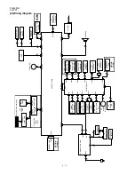
(3) Modem block
The block is mainly composed of the G3 FAX modem FM336PLus (IC30),
and is provided with the following modem function.
1) G3 FAX modem
The modem satisfies the requirements specified in ITU-T recommenda-
tions V.34 half-duplex, V.17, V.33, V.29, V.27 ter, V.21, and meets the
binary signaling requirements of V.8 and T.30 with Annex F.
Internal HDLC support eliminates the need for an external serial input/
output (SIO) device in the DTE for products incorporating error detec-
tion and T.30 protocol. The modem can perform HDLC framing per T.30
at all data speeds. CRC generation/checking along with zero insertion/
deletion enhances SDLC/HDLC frame operations. Two FSK (V.21 Ch. 1
and V.21 Ch. 2) flag pattern detectors facilitate FSK detection during
high-speed reception. The modem features a programmable DTMF trans-
mitter/receiver and three programmable tone detectors.
2) Features
· 2-wire half-duplex fax modem modes with send and receive data rates
up to 33.6 kbps.
— V.34 half-duplex, V.17, V.33, V.29, V.27 ter, and V.21 Channel 2
— Short train option in V.17 and V.27 ter
· 2-wire duplex data modem modes
— V.21, V.23 (75 bps TX/1200 bps RX or 1200 bps TX/75 bps RX)
· PSTN session starting
— V.8 and V.8 bis signaling
· HDLC support at all speeds
— Flag generation, 0-bit stuffing, ITU-T CRC-16 or CRC-32
calculation and generation
— Flag detection, 0-bit stuffing, ITU-T CRC-16 or CRC-32 check sum
error detection
— FSK flag pattern detection during high-speed receiving
· Tone modes and features
— Programmable single or dual tone generation
— DTMF receiver
— Tone detection with three programmable tone detectors
· Serial and parallel synchronous data
· Automatic Rate Adaptation (ARA) in V.34 half-duplex
· Auto-dial and auto-answer control
· TTL and CMOS compatible DTE interface
— ITU-T V.24 (EIA/TIA-232-E) (data/control)
— Microprocessor bus (data/configuration/control)
· Receive dynamic range:
— 0 dBm to -43 dBm for V.17, V.33, V.29, V.27 ter and V.21
— -9 dBm to -43 dBm for V.34 half-duplex
· Caller ID Demodulation
· Single tone detection in Data Mode
· ADPCM Voice Mode (Conexant Proprietary)
· Programmable RSLD turn-on and turn-off thresholds
· Programmable transmit level: 0 to -15 dBm
· Adjustable speaker output to monitor received signal
· DMA support for interrupt lines
· Two 16-byte FIFO data buffers for burst data transfer with extension up
to 255 bytes
· Diagnostic capability
· V.21 Channel 1 Flag detect and V.21 Channel 2 Flag detect
· +3.3 V operation with +5 V tolerant inputs
· +5 V analog signal interface
· 100-pin PQFP package
· Typical power consumption
— Normal mode:
VDD1 = 250 mW (+3.3 V for DSP); VDD = 35 mW (+5 V for IA)
— Sleep mode:
VDD1 = 20 mW (+3.3 V for DSP); VDD = 0.1 mW (+5 V for IA)
(2) Backup memory block
This block consists of flash memory for the image memory and 256 Kbit
SRAM backed up with a battery.
The image memory has a standard capacity of 2 Mbytes, and it is possi-
ble to extend the memory to 10 Mbytes in total by installing the option
memory FO-8MK to the connector CNOP1.
1) TC58V64BFT (IC27) ... pin-44, TSOP (64 Mbit NAND EEPROM)
This is non-volatile memory whose contents are not deleted even when
the power is turned off. 2 Mbytes are available as an area for storing the
encoded data of the copies or transmitted/received images.
It is controlled via the above-mentioned MAIN ASIC (IC6).
2) BS62LV256SC-70 (IC19) ... pin-28, SOP (256 Kbit SRAM)
Operation information before shutting off the power supply, user setting
content and soft switch content are stored. Even if the power supply of
the main body is turned off, it is backed up with a lithium battery (BAT1).
Содержание FO 4400 - B/W Laser - All-in-One
Страница 125: ...FO 4400U FO CS1 Control PWB parts layout Top side 6 16 ...
Страница 126: ...FO 4400U FO CS1 Control PWB parts layout Bottom side 6 17 ...
Страница 128: ...FO 4400U FO CS1 LIU PWB parts layout Top side 6 19 ...
Страница 129: ...FO 4400U FO CS1 LIU PWB parts layout Bottom side 6 20 ...
Страница 132: ...FO 4400U FO CS1 Printer PWB parts layout Top side 6 23 ...
Страница 133: ...FO 4400U FO CS1 Printer PWB parts layout Bottom side 6 24 ...
Страница 135: ...FO 4400U FO CS1 Power Supply PWB parts layout 6 26 The Power supply PWB of this model employs lead free solder ...
Страница 143: ...FO 4400U FO CS1 M E M O 6 34 ...


