FO-4400U
FO-CS1
5 – 17
[SIgnals for status recognition according to input signals]
Signal Name
Function
XCI0
XEXHS0
Incoming call (CI) detection signal
H: The handset or external telephone is in the
on-hook state.
L: The handset or external telephone in the off-
hook state.
[Other signals]
Signal Name
Function
TXOUT
RXIN
Transmission (DTMF) analog signal output from
modem
Reception (DTMF, others) analog signal input into
modem
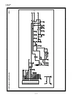
8. CI detection circuit
The CI detection circuit detects the CI signals of 15.3 Hz to 68 Hz.
A CI signal, which is provided to the photo-coupler PC1 through the
C1 (0.82 uF), R6 (22K), and ZD3 and R5 (13K) when the ring signal is
inputted from the telephone line.
9. Power supply and bias circuits
The voltages of +5V and +24VA are supplied from the control PWB
unit.
4. CML relay
The CML relay switches over connection to the matching transformer
T1 while the FAX is being used.
5. Matching transformer
The matching transformer performs electrical insulation from the tel-
ephone line and impedance matching for transmitting the FAX signal.
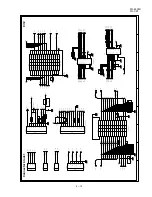
6. Hybrid circuit
The hybrid circuit performs 2-wire-to-4-wire conversion using the IC
of operational amplifier, transmits the voice transmission signal to the
line, and feeds back the voice signal to the voice reception circuit as
the side tone.
7. Signal selection
The following signals are used to control the transmission line of FAX
signal. For details, refer to the signal selector matrix table.
NO
Signal Name(CNLIU)
1
RXIN
2
TXOUT
3
CI
4
EXHS
5
DPON (N.C.)
NO
Signal Name(CNLIU)
6
CML
7
+5V
8
DG
9
+24VA
[Control signals from output port]
Signal Name
Description
CML0
SP MUTE
VOL A
VOL B
VOL C
(the circuit is located in
the control PWB.)
Line connecting relay and DP generating relay
H: Line make
L: Line brake
Speaker tone mute control signal
H: Muting (Power down mode)
L: Muting cancel (Normal operation)
Speaker volume control signal,
L
H
L
VOL A
L
L
L
VOL B
L
L
H
VOL C
VRSEL1 VRSEL2 matrix
–
High
Low
Buzzer DTMF
High
Middle
Low
High
Middle
Low
RING./
Receiving
BZCONT
(the circuit is located in
the control PWB.)
Speaker output signal switching
L: Buzzer signal output
H: When monitoring line signal
SURGE
PROTECTION
CIRCUIT
HS
DETECTOR
DIODE
BRIDGE
ACTIVE
CHOKE
HI
LO
CI
DETECTOR
+5V
TXA2
MODEM
(FM336PLUS)
RIN
SPKR
TXA1
VREF
RXIN
RXIN
TXOUT
CONTROL
LIU
HI
HI
HI
XCI0
XCI0
XEXHS0
XEXHS0
CML0
CML0
CML0
XESHS0
XCI0
MONSEL
BZOUTEN
SUB ASIC
BZCONT
SPMUTE
VOLC
VOLB
VOLA
HI
LO
LO
LO
LO
TXOUT
+5V
+24VA
DG
LINE
EXT.TEL
SPEAKER
(Example: Fax signal send)
Fig. 9
Содержание FO 4400 - B/W Laser - All-in-One
Страница 125: ...FO 4400U FO CS1 Control PWB parts layout Top side 6 16 ...
Страница 126: ...FO 4400U FO CS1 Control PWB parts layout Bottom side 6 17 ...
Страница 128: ...FO 4400U FO CS1 LIU PWB parts layout Top side 6 19 ...
Страница 129: ...FO 4400U FO CS1 LIU PWB parts layout Bottom side 6 20 ...
Страница 132: ...FO 4400U FO CS1 Printer PWB parts layout Top side 6 23 ...
Страница 133: ...FO 4400U FO CS1 Printer PWB parts layout Bottom side 6 24 ...
Страница 135: ...FO 4400U FO CS1 Power Supply PWB parts layout 6 26 The Power supply PWB of this model employs lead free solder ...
Страница 143: ...FO 4400U FO CS1 M E M O 6 34 ...


