610
Chapter 15
Asynchronous Serial Interface C (UARTC)
User’s Manual U16580EE3V1UD00
15.2 Configuration
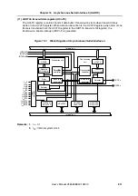
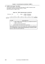
(1)
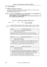
UARTCn control register 0 (UCnCTL0)
The UCnCTL0 register is an 8-bit register used to specify the asynchronous serial interface
operation.
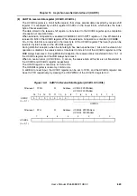
(2)
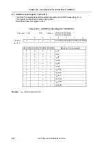
UARTCn control register 1 (UCnCTL1)
The UCnCTL1 register is an 8-bit register used to select the input clock for the asynchronous
serial interface.
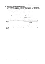
(3)
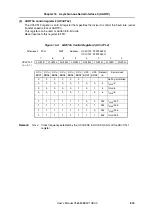
UARTCn control register 2 (UCnCTL2)
The UCnCTL2 register is an 8-bit register used to control the baud rate for the asynchronous serial
interface.
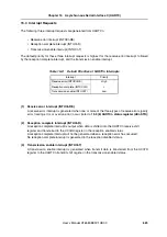
(4)
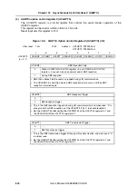
UARTCn option control register 0 (UCnOPT0)
The UCnOPT0 register is an 8-bit register used to control serial transfer for the asynchronous
serial interface.
(5)
UARTCn option control register 1 (UCnOPT1)
The UCnOPT1 register is an 8-bit register used to control the extension bit operation.
(6)
UARTCn status register (UCnSTR)
The UCnSTR register consists of flags indicating the error contents when a reception error occurs.
Each one of the reception error flags is set (to 1) upon occurrence of a reception error and is reset
(to 0) by reading the UCnSTR register.
(7)
UARTCn status register 1 (UCnSTR1)
The UCnSTR1 register indicates the operating status during a reception.
(8)
UARTCn receive shift register
This is a shift register used to convert the serial data input to the RXDCn pin into parallel data.
Upon reception of 1 byte of data and detection of the stop bit, the receive data is transferred to the
UCnRX register.
This register cannot be manipulated directly.
(9)
UARTCn receive data register (UCnRX)
The UCnRX register is an 8-bit register that holds receive data. When 7 characters are received, 0
is stored in the highest bit (when LSB first received).
In the reception enabled status, receive data is transferred from the UARTCn receive shift register
to the UCnRX register in synchronization with the completion of shift-in processing of 1 frame.
Transfer to the UCnRX register also causes reception complete interrupt (INTUCnR) to be output.
(10) UARTCn transmit shift register
The transmit shift register is a shift register used to convert the parallel data transferred from the
UCnTX register into serial data.
When 1 byte of data is transferred from the UCnTX register, the shift register data is output from
the TXDCn pin.
This register cannot be manipulated directly.
Содержание V850E/PH2
Страница 6: ...6 Preface User s Manual U16580EE3V1UD00...
Страница 16: ...16 User s Manual U16580EE3V1UD00...
Страница 28: ...28 User s Manual U16580EE3V1UD00...
Страница 32: ...32 User s Manual U16580EE3V1UD00...
Страница 84: ...84 Chapter 2 Pin Functions User s Manual U16580EE3V1UD00 MEMO...
Страница 144: ...144 Chapter 3 CPU Functions User s Manual U16580EE3V1UD00 MEMO...
Страница 192: ...192 Chapter 5 Memory Access Control Function PD70F3187 only User s Manual U16580EE3V1UD00 MEMO...
Страница 312: ...312 Chapter 9 16 Bit Timer Event Counter P User s Manual U16580EE3V1UD00 MEMO...
Страница 534: ...534 Chapter 11 16 bit Timer Event Counter T User s Manual U16580EE3V1UD00...
Страница 969: ...969 Chapter 20 Port Functions User s Manual U16580EE3V1UD00 MEMO...
Страница 970: ...970 Chapter 20 Port Functions User s Manual U16580EE3V1UD00...
Страница 976: ...976 Chapter 22 Internal RAM Parity Check Function User s Manual U16580EE3V1UD00 MEMO...
Страница 984: ...984 Chapter 23 On Chip Debug Function OCD User s Manual U16580EE3V1UD00 MEMO...
Страница 1006: ...1006 Chapter 24 Flash Memory User s Manual U16580EE3V1UD00 MEMO...
Страница 1036: ...1036 Chapter 27 Recommended Soldering Conditions User s Manual U16580EE3V1UD00 MEMO...
Страница 1046: ...1046 Appendix A Index User s Manual U16580EE3V1UD00 MEMO...
Страница 1052: ...1052 User s Manual U16580EE3V1UD00...
Страница 1053: ......

