678
Chapter 17
Clocked Serial Interface 3 (CSI3)
User’s Manual U16580EE3V1UD00
17.2 Configuration
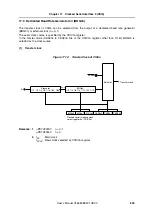
CSI3n is controlled by the clocked serial interface mode register 3n (CSIM3n).
(1)
Clocked serial interface mode register 3n (CSIM3n)
The CSIM3n register is an 8-bit register for specifying the operation of CSI3n.
(2)
Clocked serial interface clock select register 3n (CSIC30, CSIC31)
The CSIC3n register is an 8-bit register for controlling the operation clock and operating mode of
CSI3n.
(3)
Serial I/O shift register 3n (SIO3n)
The SIO3n register is an 8-bit register for converting between serial data and parallel data. SIO3n
is used for both transmission and reception.
Data is shifted in (reception) or shifted out (transmission) beginning at either the MSB side or the
LSB side.
(4)
Receive data buffer register 3n (SIRB3n)
The SIRB3n register is a 16-bit buffer register that stores receive data. This register is also divided
into two registers: the higher 8 bits (SIRB3nH) and lower 8 bits (SIRB3nL).
(5)
Chip select CSI buffer register 3n (SFCS3n)
The SFCS3n register is a 16-bit buffer register that stores chip select data. The lower 8 bits can
also be accessed by an 8-bit buffer register (SFCS3nL).
(6)
Transmit data CSI buffer register 3n (SFDB3n)
The SFDB3n register is a 16-bit buffer register that stores transmit data. This register is also
divided into two registers: the higher 8 bits (SFDB3nH) and lower 8 bits (SFDB3nL).
(7)
CSIBUF status register 3n (SFA3n)
The SFA3n register is an 8-bit register that indicates the status of CSI data buffer register n
(CSIBUFn) or the transfer status.
(8)
Transfer data length select register 3n (CSIL3n)
The CSIL3n register is an 8-bit register that selects the CSI3n transfer data length.
(9)
Transfer data number specification register 3n (SFN3n)
The SFN3n register is an 8-bit register that sets the number of CSI3n transfer data in consecutive
mode.
(10) CSI data buffer register n (CSIBUFn)
By consecutively writing transmit data to the SFDB3n register from where it is transferred, the data
can be stored in the CSIBUFn register while the CSIBUFn pointer for writing is automatically
incremented (CSIBUFn).
The CSIBUFn is a 16-bit buffer register.
Remark:
μ
PD70F3187:
n = 0, 1
μ
PD70F3447:
n = 0
Содержание V850E/PH2
Страница 6: ...6 Preface User s Manual U16580EE3V1UD00...
Страница 16: ...16 User s Manual U16580EE3V1UD00...
Страница 28: ...28 User s Manual U16580EE3V1UD00...
Страница 32: ...32 User s Manual U16580EE3V1UD00...
Страница 84: ...84 Chapter 2 Pin Functions User s Manual U16580EE3V1UD00 MEMO...
Страница 144: ...144 Chapter 3 CPU Functions User s Manual U16580EE3V1UD00 MEMO...
Страница 192: ...192 Chapter 5 Memory Access Control Function PD70F3187 only User s Manual U16580EE3V1UD00 MEMO...
Страница 312: ...312 Chapter 9 16 Bit Timer Event Counter P User s Manual U16580EE3V1UD00 MEMO...
Страница 534: ...534 Chapter 11 16 bit Timer Event Counter T User s Manual U16580EE3V1UD00...
Страница 969: ...969 Chapter 20 Port Functions User s Manual U16580EE3V1UD00 MEMO...
Страница 970: ...970 Chapter 20 Port Functions User s Manual U16580EE3V1UD00...
Страница 976: ...976 Chapter 22 Internal RAM Parity Check Function User s Manual U16580EE3V1UD00 MEMO...
Страница 984: ...984 Chapter 23 On Chip Debug Function OCD User s Manual U16580EE3V1UD00 MEMO...
Страница 1006: ...1006 Chapter 24 Flash Memory User s Manual U16580EE3V1UD00 MEMO...
Страница 1036: ...1036 Chapter 27 Recommended Soldering Conditions User s Manual U16580EE3V1UD00 MEMO...
Страница 1046: ...1046 Appendix A Index User s Manual U16580EE3V1UD00 MEMO...
Страница 1052: ...1052 User s Manual U16580EE3V1UD00...
Страница 1053: ......


