174
Chapter 4
Bus Control Function (
μ
PD70F3187 only)
User’s Manual U16580EE3V1UD00
4.6 Wait
Function
4.6.1 Programmable
wait
function
(1)
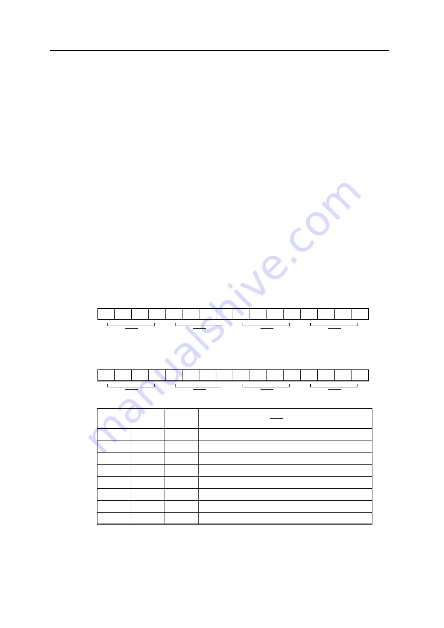
Data wait control registers 0, 1 (DWC0, DWC1)
To facilitate interfacing with low-speed memory or with I/Os, it is possible to insert up to 7 data wait
states with respect to the starting bus cycle for each CS area.
The number of wait states can be specified by data wait control registers 0 and 1 (DWC0, DWC1)
in programming. Just after system reset, all blocks have 7 data wait states inserted.
These registers can be read/written in 16-bit units.
Cautions: 1. The internal ROM area (flash memory) and the internal RAM area are not subject
to programmable waits and ordinarily no wait access is carried out. The internal
peripheral I/O area is also not subject to programmable wait states, with wait
control performed only by each peripheral function.
2. Write to the DWC0 and DWC1 registers after reset, and then do not change the set
values. Also, do not access an external memory area other than that for this
initialization routine until initial setting of the DWC0 and DWC1 registers is
finished. However, it is possible to access external memory areas whose
initialization has been finished.
Figure 4-8:
Data Wait Control Registers 0, 1 (DWC0, DWC1) Format
Remark:
n = 0 to 7
After reset:
7777H
R/W
Address:
FFFFF484H
15
14
13
12
11
10
9
8
7
6
5
4
3
2
1
0
DWC0
0
DW32 DW31 DW30
0
DW22 DW21 DW20
0
DW12 DW11 DW10
0
DW02 DW01 DW00
CS3
CS2
CS1
CS0
After reset:
7777H
R/W
Address:
FFFFF486H
15
14
13
12
11
10
9
8
7
6
5
4
3
2
1
0
DWC1
0
DW72 DW71 DW70
0
DW62 DW61 DW60
0
DW52 DW51 DW50
0
DW42 DW41 DW40
CS7
CS6
CS5
CS4
DWCn2
DWCn1
DWCn0
Number of Inserted Data Wait States
During CSn Area Access
0
0
0
No wait states inserted
0
0
1
1
0
1
0
2
0
1
1
3
1
0
0
4
1
0
1
5
1
1
0
6
1
1
1
7
Содержание V850E/PH2
Страница 6: ...6 Preface User s Manual U16580EE3V1UD00...
Страница 16: ...16 User s Manual U16580EE3V1UD00...
Страница 28: ...28 User s Manual U16580EE3V1UD00...
Страница 32: ...32 User s Manual U16580EE3V1UD00...
Страница 84: ...84 Chapter 2 Pin Functions User s Manual U16580EE3V1UD00 MEMO...
Страница 144: ...144 Chapter 3 CPU Functions User s Manual U16580EE3V1UD00 MEMO...
Страница 192: ...192 Chapter 5 Memory Access Control Function PD70F3187 only User s Manual U16580EE3V1UD00 MEMO...
Страница 312: ...312 Chapter 9 16 Bit Timer Event Counter P User s Manual U16580EE3V1UD00 MEMO...
Страница 534: ...534 Chapter 11 16 bit Timer Event Counter T User s Manual U16580EE3V1UD00...
Страница 969: ...969 Chapter 20 Port Functions User s Manual U16580EE3V1UD00 MEMO...
Страница 970: ...970 Chapter 20 Port Functions User s Manual U16580EE3V1UD00...
Страница 976: ...976 Chapter 22 Internal RAM Parity Check Function User s Manual U16580EE3V1UD00 MEMO...
Страница 984: ...984 Chapter 23 On Chip Debug Function OCD User s Manual U16580EE3V1UD00 MEMO...
Страница 1006: ...1006 Chapter 24 Flash Memory User s Manual U16580EE3V1UD00 MEMO...
Страница 1036: ...1036 Chapter 27 Recommended Soldering Conditions User s Manual U16580EE3V1UD00 MEMO...
Страница 1046: ...1046 Appendix A Index User s Manual U16580EE3V1UD00 MEMO...
Страница 1052: ...1052 User s Manual U16580EE3V1UD00...
Страница 1053: ......


