549
Chapter 12
16-bit 2-Phase Encoder Input Up/Down Counter/General Purpose Timer (TMENC10)
User’s Manual U16580EE3V1UD00
(4)
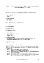
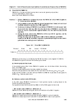
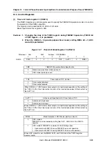
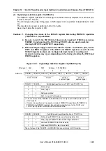
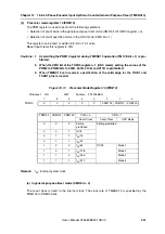
Signal edge selection register 10 (SESA10)
The SESA10 register specifies the valid edge of external interrupt requests from external pins
(TICC10, TICC11, TCLR1).
The valid edge (rising edge, falling edge, or both edges) can be specified independently for each
pin.
This register can be read or written in 8-bit or 1-bit units.
Reset input clears this register to 00H.
Cautions: 1. Changing the values of the SESA10 register bits during TMENC10 operation
(TM1CE bit = 1) is prohibited.
2. Be sure to set (1) the TM1CE bit of timer control register 1 (TMC10) even when
TMENC10 is not used and the TICC10 and TICC11 pins are used as external
interrupts INTCC10 and INTCC11 respectively.
3. Before setting the trigger mode of the TICC10, TICC11, and TCLR1n pins, set the
PM10 and PMC10 registers. If the PM10 and PMC10 registers are set after the
SESA10 register has been set, an illegal interrupt, incorrect counting, and
incorrect clearing may occur, depending on the timing of setting the PM10 and
PMC10 registers.
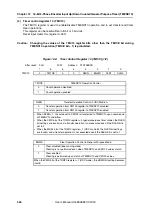
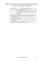
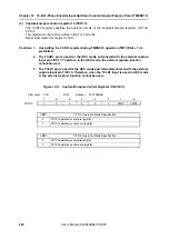
Figure 12-10:
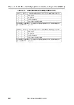
Signal Edge Selection Register 10 (SESA10) (1/2)
After reset:
00H
R/W
Address:
FFFFF6BDH
7
6
5
4
3
2
1
0
SESA10
TESUD1
TESUD0
CESUD1
CESUD0
IES111
IES110
IES101
IES100
TIUD, TCUD1
TCLR1
TICC11
capture trigger
TICC10
capture trigger
TESUD1
TESUD0
Valid Edge Specification of TIUD1 and TCUD1 Pins
0
0
Falling edge
0
1
Rising edge
1
0
Setting prohibited
1
1
Both, rising and falling edges
•
The set values of the TESUD1 and TESUD0 bits are only valid in UDC mode A and
UDC mode B.
•
If mode 4 is specified as the operation mode of TMENC10 (specified with PRM102 to
PRM100 bits of PRM10 register), the valid edge specifications for the TIUD1 and
TCUD1 pins (TESUD1 and TESUD0 bits) are not valid.
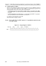
CESUD1
CESUD0
Valid Edge and Level Specification of TCLR1 Pins
0
0
Falling edge (TMENC10 cleared after edge detection)
0
1
Rising edge (TMENC10 cleared after edge detection)
1
0
Low level (TMENC10 clear status held)
1
1
High level (TMENC10 clear status held)
The set values of the CESUD1 and CESUD0 bits are valid only in UDC mode A.
Содержание V850E/PH2
Страница 6: ...6 Preface User s Manual U16580EE3V1UD00...
Страница 16: ...16 User s Manual U16580EE3V1UD00...
Страница 28: ...28 User s Manual U16580EE3V1UD00...
Страница 32: ...32 User s Manual U16580EE3V1UD00...
Страница 84: ...84 Chapter 2 Pin Functions User s Manual U16580EE3V1UD00 MEMO...
Страница 144: ...144 Chapter 3 CPU Functions User s Manual U16580EE3V1UD00 MEMO...
Страница 192: ...192 Chapter 5 Memory Access Control Function PD70F3187 only User s Manual U16580EE3V1UD00 MEMO...
Страница 312: ...312 Chapter 9 16 Bit Timer Event Counter P User s Manual U16580EE3V1UD00 MEMO...
Страница 534: ...534 Chapter 11 16 bit Timer Event Counter T User s Manual U16580EE3V1UD00...
Страница 969: ...969 Chapter 20 Port Functions User s Manual U16580EE3V1UD00 MEMO...
Страница 970: ...970 Chapter 20 Port Functions User s Manual U16580EE3V1UD00...
Страница 976: ...976 Chapter 22 Internal RAM Parity Check Function User s Manual U16580EE3V1UD00 MEMO...
Страница 984: ...984 Chapter 23 On Chip Debug Function OCD User s Manual U16580EE3V1UD00 MEMO...
Страница 1006: ...1006 Chapter 24 Flash Memory User s Manual U16580EE3V1UD00 MEMO...
Страница 1036: ...1036 Chapter 27 Recommended Soldering Conditions User s Manual U16580EE3V1UD00 MEMO...
Страница 1046: ...1046 Appendix A Index User s Manual U16580EE3V1UD00 MEMO...
Страница 1052: ...1052 User s Manual U16580EE3V1UD00...
Страница 1053: ......

