


CHAPTER 11 SERIAL INTERFACE FUNCTION
User’s Manual U15109EJ3V0UD
373
11.5.1 Configuration
I
2
Cn includes the following hardware (n = 0, 1).
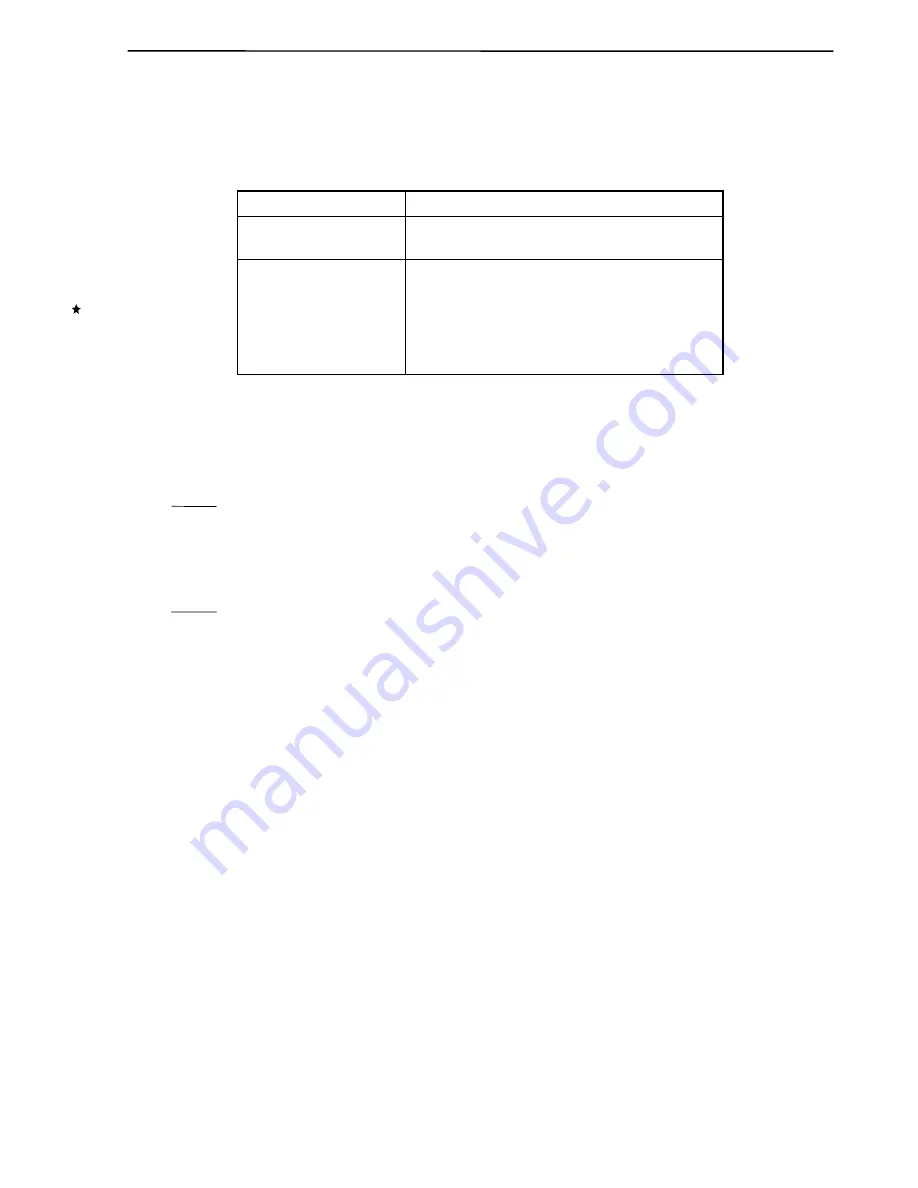
Table 11-6. Configuration of I
2
Cn
Item
Configuration
Registers
IIC shift registers 0 and 1 (IIC0, IIC1)
Slave address registers 0 and 1 (SVA0, SVA1)
Control registers
IIC control registers 0 and 1 (IICC0, IICC1)
IIC status registers 0 and 1 (IICS0, IICS1)
IIC flag registers 0 and 1 (IICF0, IICF1)
IIC clock expansion registers 0 and 1 (IICCE0, IICCE1)
IIC function expansion registers 0 and 1 (IICX0, IICX1)
IIC clock select registers 0 and 1 (IICCL0, IICCL1)
(1) IIC shift registers 0 and 1 (IIC0, IIC1)
These registers are used to convert 8-bit serial data to 8-bit parallel data and to convert 8-bit parallel data to
8-bit serial data, and can be used for both transmission and reception (n = 0, 1).
Write and read operations to IICn are used to control the actual transmit and receive operations.
IICn is set by an 8-bit memory manipulation instruction.
RESET input sets the IIC0 and IIC1 to 00H.
(2) Slave address registers 0 and 1 (SVA0, SVA1)
This register sets local addresses when in slave mode.
SVAn is set by an 8-bit memory manipulation instruction (n = 0, 1).
RESET input sets the SVA0 and SVA1 to 00H.
(3) SO latch
The SO latch is used to retain the output level of the SDAn pin (n = 0, 1).
(4) Wake-up controller
This circuit generates an interrupt request when the address received by this register matches the address
value set to slave address register n (SVAn) or when an extension code is received (n = 0, 1).
(5) Clock selector
This selects the sampling clock to be used.
(6) Serial clock counter
This counter counts the serial clocks that are output and the serial clocks that are input during
transmit/receive operations and is used to verify that 8-bit data was sent or received.


