67
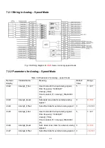
d3.28
Analog_Speed_Con
Chooses analog-speed channels
0: Invalid analog channel
1: Valid analog channel 1 (AIN1)
2: Valid analog channel 2 (AIN2)
10
~
17
:
AIN1 for ―Din_Speed (X-10)‖
20
~
27
:
AIN2 for ―Din_Speed (X-20)‖
Valid in mode -3, 3 and 1.
0
0~2
10~17
20~27
d3.29
Analog_Speed_Factor
Sets the proportion between analog signals
and output speed
0
/
d3.32
Analog_MaxT_Con
0: No control
1: Max torque that Ain1 can control
2: Max torque that Ain2 can control
0
0~2
d3.33
Analog_MaxT_Factor
Indicates the max torque factor for analog
signal control
8192
0~3276
7
7.2.3 Analog Signal Processing
Fig. 7-8 Analog signal processing
Electrical control on internal variables is available only after ADC conversion and offset of external analog
signals, and judgment of dead zone signals.
For offset processing, see the left part in Fig. 7-6; for dead zone processing, see the right part in Fig. 7-6.
7.2.4 Examples of Analog
– Speed Mode
In the analog
– speed mode, follow the steps below to set a driver:
Step 1: Confirm whether it is necessary to enable the driver through external digital input ports. To enable the
driver through external digital input ports, see Table 6-12 in Example 6-3 for settings. If the driver does not
require enabling through external digital input ports, you can disable the enabling function of external digital
input ports by referring to Table 6-13 of Example 6-3, and enable the auto power-on function of the driver by
setting its internal parameters.
Step 2: Confirm whether limit switches are required. By default, the driver operates in the limit status after
2047
-2048
shift
U
-10v
10v
1
0
2047
-2048
2
dead
U
-10v
10v
external
U
external
U
ernal
U
int
ernal
U
int
Offset
Dead zone
Содержание CD2S Series
Страница 7: ...7...
Страница 8: ...8 1 3 3 Power Brake and Encoder cable of Motors...
Страница 12: ...12 Fig 2 3 Installation direction...
Страница 15: ...15 3 1 2 Wiring Diagram Fig 3 1 Wiring diagram of CD2S driver...
Страница 16: ...16 3 1 3 X1 interface of CD2S Driver Fig 3 2 X1 interface Fig 3 3 Wiring diagram of X1 interface...
Страница 23: ...23 Fig 4 3 Separate regulation of bits...
Страница 82: ...82...
Страница 96: ...96 8 4 Debugging example 8 4 1 Oscilloscope 1 Enter oscilloscope 2 Parameters for Oscilloscope...
Страница 98: ...98 In Auto Reverse mode Kvp 110...
Страница 100: ...100 The oscilloscope is as following max following error is 69 inc Fig 2 Kpp 30 Vff 100...
Страница 101: ...101 The oscilloscope is as following max following error is 53 inc Fig 3 Kpp 30 Vff 50...
Страница 102: ...102 The oscilloscope is as following max following error is 230 inc...


