18
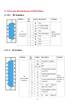
3.1.5 X5 and X6 Interfaces of CD2S Driver
3.1.5.1 X5 Interface
3.1.5.2 X6 Interface
Interface
Pin
No.
Signal Description
Function
X5
(9-pin female
connector)
1
NC
N/A
RS232
communication
interface
2
TX
To transmit data
3
RX
To receive data
4
NC
N/A
5
GND
Ground of signal
6
NC
N/A
7
NC
N/A
8
NC
N/A
9
NC
N/A
Interface
Pin
No.
Signal
Description
Function
X6
(15-pin female
connector)
1
+5V
To output 5 V voltage
Input
interface of
encoder in
motor
9
GND
0 V
8
PTC_IN N/A
2
A
To input phase-A signals
of encoder
10
/A
3
B
To input phase-B signals
of encoder
11
/B
4
Z
To input phase-Z signals
of encoder
12
/Z
5
U
To
input
phase-U
signals of encoder
13
/U
6
V
To input phase-V signals
of encoder
14
/V
7
W
To
input
phase-W
Содержание CD2S Series
Страница 7: ...7...
Страница 8: ...8 1 3 3 Power Brake and Encoder cable of Motors...
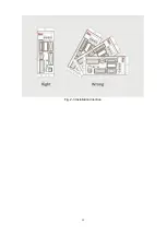
Страница 12: ...12 Fig 2 3 Installation direction...
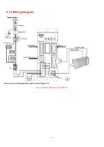
Страница 15: ...15 3 1 2 Wiring Diagram Fig 3 1 Wiring diagram of CD2S driver...
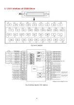
Страница 16: ...16 3 1 3 X1 interface of CD2S Driver Fig 3 2 X1 interface Fig 3 3 Wiring diagram of X1 interface...
Страница 23: ...23 Fig 4 3 Separate regulation of bits...
Страница 82: ...82...
Страница 96: ...96 8 4 Debugging example 8 4 1 Oscilloscope 1 Enter oscilloscope 2 Parameters for Oscilloscope...
Страница 98: ...98 In Auto Reverse mode Kvp 110...
Страница 100: ...100 The oscilloscope is as following max following error is 69 inc Fig 2 Kpp 30 Vff 100...
Страница 101: ...101 The oscilloscope is as following max following error is 53 inc Fig 3 Kpp 30 Vff 50...
Страница 102: ...102 The oscilloscope is as following max following error is 230 inc...


