51
0
0
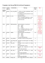
The 0 gain
Kvp 0
60F90110
Kvi 0
60F90210
Kpp 0
60FB0110
0
1
The 1
st
gain
Kvp 1
23400410
Kvi 1
23400510
Kpp 1
23400610
1
0
The 2
nd
gain
Kvp 2
23400710
Kvi 2
23400810
Kpp 2
23400910
1
1
The 3
rd
gain
Kvp 3
23400A10
Kvi 3
23400B10
Kpp 3
23400C10
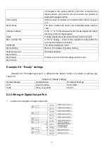
Example 6-3: Driver Enable Setting
Requirement: The ―driver enable‖ function is controlled through an external digital output port. In this
example, the digital input port DIN1 is defined as the ―driver enable‖ function. Table 6-10 shows the setup
method.
Table 6-
10 Digital Input Port DIN1 Defined as the ―Driver Enable‖ Function
Numeric Display
Variable Name
Parameter Settings
d3.01
Din1_Function
Set to 000.1
d3.00
Store_Loop_Data
Set to 1
Note: Any digital output of DIN1-
7 can be defined as ―driver enable‖, and is set to 000.1, that is, bit 0 is valid.
Requirement: Enable the function of automatically powering on the driver by setting internal parameters
in drivers instead of external digital input ports. Table 6-11 describes the setup method.
Table 6-11 Enabling the function of automatically powering on the driver by setting internal parameters in
drivers
Numeric Display
Variable Name
Parameter Settings
d3.01- d3.07
DinX_ Function
(1~7)
None of the digital input port can be
set to 000.1, that is, the Enable
function is not controlled by any
digital input port.
d3.10
Switch_On_Auto
Set to 1
d3.00
Store_Loop_Data
Set to 1
Example 6-4: Disabling Position Positive/Negative Limit Settings
When the driver is delivered, the DIN5 of the motor is the position positive limit and DIN6 is the position
negative limit by default. If there are no external position positive/negative limit switches, this function must be
disabled so that the servo driver can work properly. Table 6-12 describes the setup method.
Table 6-12: Disabling position positive/negative limit settings
Numeric
Variable Name
Parameter Settings
Содержание CD2S Series
Страница 7: ...7...
Страница 8: ...8 1 3 3 Power Brake and Encoder cable of Motors...
Страница 12: ...12 Fig 2 3 Installation direction...
Страница 15: ...15 3 1 2 Wiring Diagram Fig 3 1 Wiring diagram of CD2S driver...
Страница 16: ...16 3 1 3 X1 interface of CD2S Driver Fig 3 2 X1 interface Fig 3 3 Wiring diagram of X1 interface...
Страница 23: ...23 Fig 4 3 Separate regulation of bits...
Страница 82: ...82...
Страница 96: ...96 8 4 Debugging example 8 4 1 Oscilloscope 1 Enter oscilloscope 2 Parameters for Oscilloscope...
Страница 98: ...98 In Auto Reverse mode Kvp 110...
Страница 100: ...100 The oscilloscope is as following max following error is 69 inc Fig 2 Kpp 30 Vff 100...
Страница 101: ...101 The oscilloscope is as following max following error is 53 inc Fig 3 Kpp 30 Vff 50...
Страница 102: ...102 The oscilloscope is as following max following error is 230 inc...


