background image

Rev. 3.0, 10/02, page 307 of 686
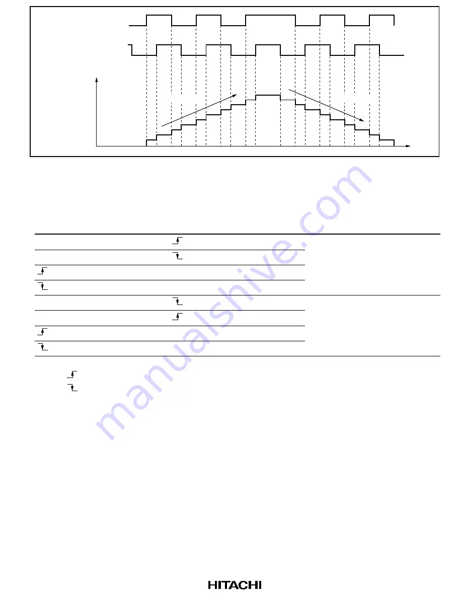
TCNT value

Time

Down-count

Up-count

TCLKA (channel 1)
TCLKC (channel 2)

TCLKB (channel 1)
TCLKD (channel 2)

Figure 10.26   Example of Phase Counting Mode 1 Operation

Table 10.20 Up/Down-Count Conditions in Phase Counting Mode 1

TCLKA (Channel 1)

TCLKC (Channel 2)

TCLKB (Channel 1)

TCLKD (Channel 2)

Operation

High level

Low level

Low level

High level

Up-count

High level

Low level

High level

Low level

Down-count

Legend:

 : Rising edge

 : Falling edge

2. Phase counting mode 2

Figure 10.27 shows an example of phase counting mode 2 operation, and table 10.21
summarizes the TCNT up/down-count conditions.

Содержание H8S/2215 Series

Страница 1: ...Hitachi Single Chip Microcomputer H8S 2215 Series Hardware Manual ADE 602 217B Rev 3 0 10 04 02 Hitachi Ltd ...

Страница 2: ...e or cause risk of bodily injury such as aerospace aeronautics nuclear power combustion control transportation traffic safety equipment or medical equipment for life support 4 Design your application so that the product is used within the ranges guaranteed by Hitachi particularly for maximum rating operating supply voltage range heat radiation characteristics installation conditions and other char...

Страница 3: ...nitialization Note When power is first supplied the product s state is undefined The states of internal circuits are undefined until full power is supplied throughout the chip and a low level is input on the reset pin During the period where the states are undefined the register settings and the output state of each pin are also undefined Design your system so that it does not malfunction because ...

Страница 4: ...Rev 3 0 10 02 page iv of lviii ...

Страница 5: ...e Points for Caution When designing an application system that includes this LSI take the points for caution into account Each section includes points for caution in relation to the descriptions given and points for caution in usage are given as required as the final part of each section 7 List of Registers 8 Electrical Characteristics 9 Appendix Product type codes and external dimensions Major re...

Страница 6: ...Rev 3 0 10 02 page vi of lviii ...

Страница 7: ...ion are available for this LSI s ROM The F ZTAT version provides flexibility as it can be reprogrammed in no time to cope with all situations from the early stages of mass production to full scale mass production This is particularly applicable to application devices with specifications that will most probably change This manual describes this LSI s hardware Note F ZTAT TM is a trademark of Hitach...

Страница 8: ...rder The MSB is on the left and the LSB is on the right Related Manuals The latest versions of all related manuals are available from our web site Please ensure you have the latest versions of all documents you require http www hitachisemiconductor com H8S 2215 Series manuals Manual Title ADE No H8S 2215 Series Hardware Manual This manual H8S 2600 Series H8S 2000 Series Programming Manual ADE 602 ...

Страница 9: ...5B 128 kbytes 16 kbytes Masked ROM Version HD6432215C 64 kbytes 8 kbytes Remarks column amended Incorrect Under development Correct 1 2 Internal Block Diagram Figure 1 1 Internal Block Diagram 2 Figure amended Interrupts controller USB NMI FWE USPND USD USD VBUS Note added to figure Note The FWE pin is only provided in the flash memory version 1 3 Pin Arrangement Figure 1 2 Pin Arrangement TFP 120...

Страница 10: ...3 TCK P42 AN2 P43 AN3 PG1 PG2 PG0 USPND Vref P40 AN0 P41 AN1 P71 MD2 NMI PLLVCC DrVCC VBUS AVCC P36 PF5 XTAL MD0 DrVSS USD P34 RxD1 P33 TxD1 P30 TxD0 PF2 PF6 EXTAL VSS MD1 XTAL48 PLLVSS USD Reserve P31 RxD0 PF1 PF4 PF7 VCC FWE EXTAL48 PLLCAP Reserve Note added Note The FWE pin is only provided in the flash memory version 1 5 Pin Functions 11 Table amended Pin No Type Symbol TFP 120 BP 112 I O Func...

Страница 11: ... 1111 Table 9 9 P10 Pin Function Address amended Incorrect Other than B 1111 Correct Other than B 1101 to B 1111 9 2 5 Pin Functions Table 9 13 P33 Pin Function 227 Pin function amended TE 0 1 P33DDR 0 1 Pin function P33 input P33 output TxD1 output Table 9 16 P30 Pin Function 228 Pin function amended TE 0 1 P30DDR 0 1 Pin function P30 input P30 output TxD0 output 9 8 3 Port C Register PORTC 244 N...

Страница 12: ...MHz Base clock 16 MHz 2 8 MHz 8 MHz 18 25 5 76 MHz average Base clock with 460 784 kbps average transfer rate Average transfer rate 7 3725 MHz 16 460 784 kbps Average error 0 004 Average transfer rate 5 76 MHz 8 720 kbps Average error 0 Base clock with 720 kbps average transfer rate 5 76 MHz 1 bit base clock 8 1 2 3 4 5 6 7 8 1 2 3 2 MHz 1 8431 MHz 1 bit base clock 16 Base clock 16 MHz 8 2 MHz 2 M...

Страница 13: ...OR_1 H 21 1 output on TGRB_1 compare match TIOCA1 initial output 0 0 output on TGRA_1 compare match TCR_2 H 2C TCNT_2 incremented on falling edge of TCLKA TIOCA1 TCNT_2 cleared by TGRA_2 compare match TGRB_2 H 0000 TGRA_2 H 000C TIOR_2 H 21 1 output on TGRB_2 compare match TIOCA2 initial output 0 0 output on TGRA_2 compare match SEMR_0 H 0C ABCS 1 ACS2 0 B 100 Main clock 16 MHz TIOCA1 TPU_1 output...

Страница 14: ...codes H 0002200F H 0003200F H 001B200F and H 001C200F respectively from the TDO Table 14 3 IDCODE Register Configuration Code amended Incorrect HD64F2215 code Correct HD64F2215 code HD64F2215U code 15 1 Features Endpoint configuration selectable 433 Replaced The FIFO buffer for bulk transfer and isochronous transfer has a double buffer configuration Total 1288 byte FIFO EP0s fixed Control_setup FI...

Страница 15: ...EPIRnn_0 Bit Bit Name Initial Value R W Description 7 to4 D39 D36 R W Endpoint number 4 bit configuration settable values 0 to 8 0000 Control transfer EP0 0001 to 1000 Other than Control transfer EP1 to EP8 There are restrictions on settable endpoint numbers according to the Interface number and Alternate number to which the endpoint belongs Restriction 1 Set different endpoint numbers under one A...

Страница 16: ...r 0 or 64 UEPIR02 UEPIR03 UEPIR20 UEPIR21 Isochronous transfer 0 to 128 UEPIR04 to UEPIR19 UEPIRnn_2 440 UEPIRnn_2 Bit Bit Name Initial Value R W Description 7 to 0 D23 D16 R W Endpoint maximum packet size D25 to D16 10 bit configuration Control transfer 64 only UEPIR00 Interrupt transfer 0 to 64 UEPIR01 UEPIR22 Bulk transfer 0 or 64 UEPIR02 UEPIR03 UEPIR20 UEPIR21 Isochronous transfer 0 to 128 UE...

Страница 17: ...Endpoint2i 15 3 16 USB Endpoint Data Register 2o UEDR2o 14th line changed as follows Incorrect Endpoint2 Correct Endpoint2o 15 3 17 USB Endpoint Data Register 3i UEDR3i 459 2nd line changed as follows Incorrect Endpoint3 Correct Endpoint3i 15 3 18 USB Endpoint Data Register 3o UEDR3o 9th line changed as follows Incorrect Endpoint3 Correct Endpoint3o 15 3 19 USB Endpoint Data Register 4i UEDR4i 15t...

Страница 18: ...t4o 14 th line changed as follows Incorrect The FIFO for endpoint 4 out transfer has a dual FIFO configuration Correct The FIFO for endpoint 4o for Bulk_out transfer has a dual FIFO configuration 15 3 30 USB Interrupt Enable Register 0 UIER0 470 Bit table amended 5 EP1iTRE 0 R W Enables the EP1iTR interrupt Bit Bit Name Initial Value R W Description 7 BRSTE 0 R W Enables the BRST interrupt 6 0 R R...

Страница 19: ...Transceiver Input Signal Monitor Bits RCV Monitors the RCV signal of the internal external transceiver VP Monitors the VP signal of the internal external transceiver VM Monitors the VM signal of the internal external transceiver Note An asterisk indicates an undefined value 15 3 42 USB Test Register 1 UTSTR1 Table 15 4 Relationship between the UTSTR1 Settings and Pin Inputs 480 UTSTR1 Monitor valu...

Страница 20: ...om the host FIFO B FIFO A Receive SOF USB function Receive data error Yes No Yes No Switch to FIFO Receive SOF Receive OUT token Receive data error Set EP3o normal receive status to 1 Set Internal EP3o TS to 1 Set EP3o abnormal receive status to 1 Set Internal EP3o TF to 1 Set EP3o abnormal receive status to 1 Set internal EP3o TF to 1 B side UIFR1 EP3oTS EP3oTF update A side UIFR1 EP3oTS EP3oTF u...

Страница 21: ...rol pin In HD64F2215U in which on chip ROM can be programmed by using the USB P36 should be used as the D pull up control pin 3 15 9 7 EP3o Isochronous Transfer Figure 15 32 EP3o Date Reception 528 Figure amended Data 1 Modify Receive USB data 1 In frame N In frame N 1 In frame N 2 Receive USB data 2 Receive USB data 3 TS TF EP3o FIFO A EP3o FIFO B Data 1 Data 2 Modify A side flag update Data 1 ca...

Страница 22: ...cannot be modified 3 2 CKS1 CKS0 0 0 R W R W Clock Select 0 and 1 These bits specify the A D conversion time The conversion time should be changed only when ADST 0 Specify a setting that gives a value within the range shown in table 24 7 00 Conversion time 530 states max 01 Conversion time 266 states max 10 Conversion time 134 states max 11 Conversion time 68 states max The conversion time setting...

Страница 23: ... SCI boot mode With data transfer in SCI boot mode this LSI s bit rate can be automatically adjusted to match the transfer bit rate of the host 19 2 Mode Transitions Figure 19 2 Flash Memory State Transitions 559 Figure amended Boot mode SCI USB On board programming mode User program mode Table 19 1 Differences between Boot Mode and User Program Mode 560 Incorrect Boot Mode Correct SCI USB Boot Mo...

Страница 24: ...D64F2215U 19 6 On Board Programming Modes Table 19 3 Setting On Board Programming Modes 571 Incorrect Boot mode Correct SCI boot mode HD64F2215 USB boot mode HD64F2215U 19 6 1 SCI Boot Mode HD64F2215 571 to 574 Amended Incorrect Boot Mode Correct SCI Boot Mode Figure 19 6 SCI System Configuration in Boot Mode 572 Figure amended H8S 2215 Series Flash memory 1 01X MD2 to 0 FWE Note added to figure N...

Страница 25: ...lows The external clock input conditions when the duty adjustment circuit is not used are shown in table 21 4 When the duty adjustment circuit is not used note that the maximum operating frequency depends on the external clock input waveform For example if tEXL TEXH 31 25ns and tEXr tEXf 6 25 ns the maximum operating frequency becomes 13 3 MHz depending on the clcok cycle time of 75 ns 21 6 1 Conn...

Страница 26: ... ms block Reprogramming count NWEC 100 10 000 100 Times Data retention time tDRP 10 Year Notes added 6 Minimum number of times for which all characteristics are guaranteed after rewriting Guarantee range is 1 to minimum value 7 Reference value for 25 C as a guideline rewriting should normally function up to this value 8 Data retention characteristic when rewriting is performed within the specifica...

Страница 27: ...gure C 2 BP 112 Package Dimension 680 Replaced 10 00 0 40 0 05 0 2 0 10 10 00 C C 1 40 Max 0 20 C A 0 20 C B 0 80 0 80 1 00 1 00 B C 0 15 A B C D E F G H J K L 11 10 9 8 7 6 5 4 3 2 1 Unit mm A 112 φ0 50 0 05 C φ0 08 A B M 4 Hitachi Code JEDEC JEITA Mass reference value BP 112 0 3 g ...

Страница 28: ...Rev 3 0 10 02 page xxviii of lviii ...

Страница 29: ...EXR 29 2 4 4 Condition Code Register CCR 30 2 4 5 Initial Register Values 32 2 5 Data Formats 32 2 5 1 General Register Data Formats 32 2 5 2 Memory Data Formats 34 2 6 Instruction Set 35 2 6 1 Table of Instructions Classified by Function 36 2 6 2 Basic Instruction Formats 45 2 7 Addressing Modes and Effective Address Calculation 46 2 7 1 Register Direct Rn 47 2 7 2 Register Indirect ERn 47 2 7 3 ...

Страница 30: ...n Handling Types and Priority 65 4 2 Exception Sources and Exception Vector Table 65 4 3 Reset 67 4 3 1 Reset Types 67 4 3 2 Reset Exception Handling 68 4 3 3 Interrupts after Reset 69 4 3 4 State of On Chip Peripheral Modules after Reset Release 69 4 4 Traces 70 4 5 Interrupts 70 4 6 Trap Instruction 71 4 7 Stack Status after Exception Handling 72 4 8 Notes on Use of the Stack 73 Section 5 Interr...

Страница 31: ...101 6 3 Register Descriptions 101 6 3 1 Bus Width Control Register ABWCR 101 6 3 2 Access State Control Register ASTCR 102 6 3 3 Wait Control Registers H and L WCRH WCRL 103 6 3 4 Bus Control Register H BCRH 107 6 3 5 Bus Control Register L BCRL 108 6 3 6 Pin Function Control Register PFCR 109 6 4 Bus Control 110 6 4 1 Area Divisions 110 6 4 2 Bus Specifications 111 6 4 3 Bus Interface for Each Ar...

Страница 32: ... 4 2 Sequential Mode 164 7 4 3 Idle Mode 167 7 4 4 Repeat Mode 168 7 4 5 Normal Mode 172 7 4 6 Block Transfer Mode 175 7 4 7 DMAC Activation Sources 180 7 4 8 Basic DMAC Bus Cycles 181 7 4 9 DMAC Bus Cycles Dual Address Mode 182 7 4 10 DMAC Multi Channel Operation 186 7 4 11 Relation between the DMAC External Bus Requests Refresh Cycles and the DTC 187 7 4 12 NMI Interrupts and DMAC 188 7 4 13 For...

Страница 33: ...fer 210 8 5 5 Interrupts 211 8 5 6 Operation Timing 211 8 5 7 Number of DTC Execution States 212 8 6 Procedures for Using DTC 214 8 6 1 Activation by Interrupt 214 8 6 2 Activation by Software 214 8 7 Examples of Use of the DTC 215 8 7 1 Normal Mode 215 8 7 2 Software Activation 215 8 8 Usage Notes 216 8 8 1 Module Stop 216 8 8 2 On Chip RAM 216 8 8 3 DTCE Bit Setting 216 8 8 4 DMAC Transfer End I...

Страница 34: ... 237 9 7 1 Port B Data Direction Register PBDDR 238 9 7 2 Port B Data Register PBDR 238 9 7 3 Port B Register PORTB 239 9 7 4 Port B MOS Pull Up Control Register PBPCR 239 9 7 5 Pin Functions 240 9 7 6 Port B Input Pull Up MOS Function 241 9 8 Port C 243 9 8 1 Port C Data Direction Register PCDDR 243 9 8 2 Port C Data Register PCDR 243 9 8 3 Port C Register PORTC 244 9 8 4 Port C Pull Up MOS Contr...

Страница 35: ...3 Register Descriptions 268 10 3 1 Timer Control Register TCR 269 10 3 2 Timer Mode Register TMDR 273 10 3 3 Timer I O Control Register TIOR 274 10 3 4 Timer Interrupt Enable Register TIER 284 10 3 5 Timer Status Register TSR 286 10 3 6 Timer Counter TCNT 288 10 3 7 Timer General Register TGR 288 10 3 8 Timer Start Register TSTR 289 10 3 9 Timer Synchro Register TSYR 290 10 4 Interface to Bus Mast...

Страница 36: ... 5 5 Timing of TCNT External Reset 337 11 5 6 Timing of Overflow Flag OVF Setting 338 11 6 Operation with Cascaded Connection 339 11 6 1 16 Bit Counter Mode 339 11 6 2 Compare Match Count Mode 339 11 7 Interrupts 340 11 7 1 Interrupt Sources and DTC Activation 340 11 7 2 A D Converter Activation 340 11 8 Usage Notes 341 11 8 1 Contention between TCNT Write and Clear 341 11 8 2 Contention between T...

Страница 37: ...ster TSR 362 13 3 5 Serial Mode Register SMR 363 13 3 6 Serial Control Register SCR 365 13 3 7 Serial Status Register SSR 367 13 3 8 Smart Card Mode Register SCMR 370 13 3 9 Serial Extended Mode Register 0 SEMR_0 371 13 3 10 Bit Rate Register BRR 375 13 4 Operation in Asynchronous Mode 381 13 4 1 Data Transfer Format 381 13 4 2 Receive Data Sampling Timing and Reception Margin in Asynchronous Mode...

Страница 38: ...CODE Register IDCODE 422 14 3 3 BYPASS Register BYPASS 422 14 3 4 Boundary Scan Register BSCANR 422 14 4 Boundary Scan Function Operation 431 14 4 1 TAP Controller 431 14 5 Usage Notes 431 Section 15 Universal Serial Bus Interface USB 433 15 1 Features 433 15 2 Input Output Pins 436 15 3 Register Descriptions 437 15 3 1 USB Endpoint Information Registers 00_0 to 22_4 UEPIR00_0 to UEPIR22_4 438 15 ...

Страница 39: ...33 USB Interrupt Enable Register 3 UIER3 471 15 3 34 USB Interrupt Select Register 0 UISR0 472 15 3 35 USB Interrupt Select Register 1 UISR1 472 15 3 36 USB Interrupt Select Register 2 UISR2 473 15 3 37 USB Interrupt Select Register 3 UISR3 473 15 3 38 USB Data Status Register UDSR 474 15 3 39 USB Configuration Value Register UCVR 475 15 3 40 USB Time Stamp Registers H L UTSRH UTSRL 476 15 3 41 US...

Страница 40: ...15 9 10 Level Shifter for VBUS and IRQx Pins 529 15 9 11 USB Endpoint Data Read and Write 529 15 9 12 Restrictions for Software Standby Mode Transition 530 15 9 13 USB External Circuit Example 532 Section 16 A D Converter 533 16 1 Features 533 16 2 Input Output Pins 535 16 3 Register Descriptions 535 16 3 1 A D Data Registers A to D ADDRA to ADDRD 535 16 3 2 A D Control Status Register ADCSR 536 1...

Страница 41: ... EBR1 567 19 5 4 Erase Block Register 2 EBR2 568 19 5 5 RAM Emulation Register RAMER 569 19 5 6 Serial Control Register X SCRX 570 19 6 On Board Programming Modes 571 19 6 1 SCI Boot Mode HD64F2215 571 19 6 2 USB Boot Mode HD64F2215U 575 19 6 3 Programming Erasing in User Program Mode 581 19 7 Flash Memory Emulation in RAM 582 19 8 Flash Memory Programming Erasing 583 19 8 1 Program Program Verify...

Страница 42: ...tes 604 21 8 1 Note on Crystal Resonator 604 21 8 2 Note on Board Design 604 21 8 3 Note on Switchover of External Clock 605 Section 22 Power Down Modes 607 22 1 Register Descriptions 610 22 1 1 Standby Control Register SBYCR 610 22 1 2 System Clock Control Register SCKCR 612 22 1 3 Module Stop Control Registers A to C MSTPCRA to MSTPCRC 612 22 2 Medium Speed Mode 614 22 3 Sleep Mode 615 22 3 1 Tr...

Страница 43: ... Each Operating Mode 642 Section 24 Electrical Characteristics 649 24 1 Absolute Maximum Ratings 649 24 2 Power Supply Voltage and Operating Frequency Range 650 24 3 DC Characteristics 651 24 4 AC Characteristics 654 24 4 1 Clock Timing 655 24 4 2 Control Signal Timing 656 24 4 3 Bus Timing 658 24 4 4 Timing of On Chip Supporting Modules 664 24 5 UBS Characteristics 670 24 6 A D Conversion Charact...

Страница 44: ...53 Section 3 MCU Operating Modes Figure 3 1 Memory Map in Each Operating Mode for HD64F2215 HD64F2215U and HD6432215A 61 Figure 3 2 Memory Map in Each Operating Mode for HD6432215B 62 Figure 3 3 Memory Map in Each Operating Mode for HD6432215C 63 Section 4 Exception Handling Figure 4 1 Reset Sequence Modes 2 and 3 Not available in this LSI 68 Figure 4 2 Reset Sequence Mode 4 69 Figure 4 3 Stack St...

Страница 45: ...dd Address Byte Access 126 Figure 6 18 Bus Timing for 16 Bit 3 State Access Space 3 Word Access 127 Figure 6 19 Example of Wait State Insertion Timing 129 Figure 6 20 Example of Burst ROM Access Timing When AST0 BRSTS1 1 131 Figure 6 21 Example of Burst ROM Access Timing When AST0 BRSTS1 0 131 Figure 6 22 Example of Idle Cycle Operation 1 133 Figure 6 23 Example of Idle Cycle Operation 2 134 Figur...

Страница 46: ...ence between DTC Vector Address and Register Information 203 Figure 8 5 Flowchart of DTC Operation 205 Figure 8 6 Memory Mapping in Normal Mode 207 Figure 8 7 Memory Mapping in Repeat Mode 208 Figure 8 8 Memory Mapping in Block Transfer Mode 209 Figure 8 9 Chain Transfer Memory Map 210 Figure 8 10 DTC Operation Timing Example in Normal Mode or Repeat Mode 211 Figure 8 11 DTC Operation Timing Examp...

Страница 47: ...Timing 314 Figure 10 34 Counter Clear Timing Compare Match 315 Figure 10 35 Counter Clear Timing Input Capture 315 Figure 10 36 Buffer Operation Timing Compare Match 315 Figure 10 37 Buffer Operation Timing Input Capture 316 Figure 10 38 TGI Interrupt Timing Compare Match 316 Figure 10 39 TGI Interrupt Timing Input Capture 317 Figure 10 40 TCIV Interrupt Setting Timing 317 Figure 10 41 TCIU Interr...

Страница 48: ...Increment 356 Section 13 Serial Communication Interface Figure 13 1 Block Diagram of SCI_0 359 Figure 13 2 Block Diagram of SCI_1 and SCI_2 360 Figure 13 3 Examples of Base Clock when Average Transfer Rate is Selected 373 Figure 13 4 Example of Average Transfer Rate Setting with TPU Clock Input 374 Figure 13 5 Data Format in Asynchronous Communication Example with 8 Bit Data Parity Two Stop Bits 3...

Страница 49: ...ansmission Using Internal Clock 412 Figure 13 30 Sample Flowchart for Mode Transition during Reception 413 Figure 13 31 Operation when Switching from SCK Pin Function to Port Pin Function 414 Figure 13 32 Operation when Switching from SCK Pin Function to Port Pin Function Example of Preventing Low Level Output 415 Section 14 Boundary Scan Function Figure 14 1 Block Diagram of Boundary Scan Functio...

Страница 50: ...s Used 522 Figure 15 29 USB External Circuit in Bus Powered Mode When External Transceiver is Used 523 Figure 15 30 USB External Circuit in Self Powered Mode When External Transceiver is Used 524 Figure 15 31 10 Byte Data Reception 527 Figure 15 32 EP3o Data Reception 528 Figure 15 33 Transition to and from Software Standby Mode 531 Figure 15 34 USB Software Standby Mode Transition Timing 532 Sect...

Страница 51: ...onator Example 599 Figure 21 3 Crystal Resonator Equivalent Circuit 599 Figure 21 4 External Clock Input Examples 600 Figure 21 5 External Clock Input Timing 601 Figure 21 6 Connection of Ceramic Resonator 602 Figure 21 7 Connection of Ceramic Resonator 602 Figure 21 8 48 MHz External Clock Input Timing 603 Figure 21 9 Pin Handling when 48 MHz External Clock is Not Used 603 Figure 21 10 Example of...

Страница 52: ... Input Output Timing 666 Figure 24 14 TPU Clock Input Timing 666 Figure 24 15 8 bit Timer Output Timing 667 Figure 24 16 8 bit Timer Clock Input Timing 667 Figure 24 17 8 bit Timer Reset Input Timing 667 Figure 24 18 SCK Clock Input Timing 667 Figure 24 19 SCI Input Output Timing Clock Synchronous Mode 668 Figure 24 20 A D Converter External Trigger Input Timing 668 Figure 24 21 Boundary Scan TCK ...

Страница 53: ... Modes Table 3 1 MCU Operating Mode Selection 55 Table 3 2 Pin Functions in Each Operating Mode 60 Section 4 Exception Handling Table 4 1 Exception Types and Priority 65 Table 4 2 Exception Handling Vector Table 66 Table 4 3 Reset Types 67 Table 4 4 Status of CCR and EXR after Trace Exception Handling 70 Table 4 5 Status of CCR and EXR after Trap Instruction Exception Handling 71 Section 5 Interru...

Страница 54: ... Vector Addresses and Corresponding DTCE 204 Table 8 3 Overview of DTC Functions 206 Table 8 4 Register Information in Normal Mode 207 Table 8 5 Register Information in Repeat Mode 208 Table 8 6 Register Information in Block Transfer Mode 209 Table 8 7 DTC Execution Status 213 Table 8 8 Number of States Required for Each Execution Status 213 Section 9 I O Ports Table 9 1 Port Functions 1 217 Table...

Страница 55: ... PB0 Pin Function 241 Table 9 35 Input Pull Up MOS States Port B 242 Table 9 36 PC7 Pin Function 244 Table 9 37 PC6 Pin Function 245 Table 9 38 PC5 Pin Function 245 Table 9 39 PC4 Pin Function 245 Table 9 40 PC3 Pin Function 245 Table 9 41 PC2 Pin Function 245 Table 9 42 PC1 Pin Function 245 Table 9 43 PC0 Pin Function 246 Table 9 44 Input Pull Up MOS States Port C 246 Table 9 45 PD7 Pin Function ...

Страница 56: ...l 0 270 Table 10 4 CCLR2 to CCLR0 channels 1 and 2 270 Table 10 5 TPSC2 to TPSC0 channel 0 271 Table 10 6 TPSC2 to TPSC0 channel 1 271 Table 10 7 TPSC2 to TPSC0 channel 2 272 Table 10 8 MD3 to MD0 274 Table 10 9 TIORH_0 channel 0 276 Table 10 10 TIORH_0 channel 0 277 Table 10 11 TIORL_0 channel 0 278 Table 10 12 TIORL_0 channel 0 279 Table 10 13 TIOR_1 channel 1 280 Table 10 14 TIOR_1 channel 1 28...

Страница 57: ...e 13 7 Maximum Bit Rate with External Clock Input Clocked Synchronous Mode 380 Table 13 8 Serial Transfer Formats Asynchronous Mode 382 Table 13 9 SSR Status Flags and Receive Data Handling 389 Table 13 10 SCI Interrupt Sources 409 Section 14 Boundary Scan Function Table 14 1 Pin Configuration 419 Table 14 2 Instruction configuration 420 Table 14 3 IDCODE Register Configuration 422 Table 14 4 Corr...

Страница 58: ... Characteristics 599 Table 21 3 External Clock Input Conditions 600 Table 21 4 External Clock Input Conditions when Duty Adjustment Circuit is not Used 601 Table 21 5 External Clock Input Conditions when Duty Adjustment Circuit is not Used 603 Section 22 Power Down Modes Table 22 1 LSI Internal States in Each Mode 608 Table 22 2 Low Power Dissipation Mode Transition Conditions 609 Table 22 3 Oscil...

Страница 59: ...erface SCI Boundary scan Universal serial bus USB 10 bit A D converter 8 bit D A converter Clock pulse generator On chip memory ROM Product Code ROM RAM Remarks HD64F2215 256 kbytes 16 kbytes SCI boot version F ZTAT Version HD64F2215U 256 kbytes 16 kbytes USB boot version HD6432215A 256 kbytes 16 kbytes In planning HD6432215B 128 kbytes 16 kbytes Masked ROM Version HD6432215C 64 kbytes 8 kbytes Ge...

Страница 60: ...TMRI01 TMCI01 P71 P72 TMO0 P73 T M O 1 P74 PG4 PG3 PG2 PG1 PG0 PF7 PF6 PF5 PF4 PF3 PF2 PF1 PF0 MD2 MD1 MD0 EXTAL XTAL PLLVCC PLLCAP PLLVSS EXTAL48 XTAL48 Peripheral data bus Peripheral address bus P96 AN14 DA0 P97 AN15 DA1 AVCC Vref AVSS Internal data bus Port D Boundary scan PLL for USB ROM RAM TPU 3 channels D A converter 1 channel H8S 2000 CPU DTC WDT DMAC Interrupts controller USB Port E Port ...

Страница 61: ...2 A10 RESERVE PB3 A11 PB4 A12 PB5 A13 PB6 A14 PB7 A15 PA0 A16 60 59 58 57 56 55 54 53 52 51 50 49 48 47 46 45 44 43 42 41 40 39 38 37 36 35 34 33 32 31 DrVSS USD USD DrVCC VBUS RESERVE USPND RESERVE AVCC Vref P40 AN0 P41 AN1 P42 AN2 P43 AN3 P96 AN14 DA0 P97 AN15 DA1 AVSS P17 TIOCB2 TCLKD P16 TIOCA2 P15 TIOCB1 TCLKC FSE0 P14 TIOCA1 P13 TIOCD0 TCLKB A23 VPO P12 TIOCC0 TCLKA A22 RCV P11 TIOCB0 A21 VP...

Страница 62: ...5 VSS PC3 A3 PC6 A6 PB1 A9 PB4 A12 PB7 A15 Reserve PE6 D6 PD0 D8 PD3 D11 PD6 D14 PC1 A1 PC4 A4 PC7 A7 PB3 A11 PB6 A14 PE3 D3 PE5 D5 PE7 D7 PD5 D13 PC0 A0 PC2 A2 PB0 A8 PB5 A13 PA0 A16 PE0 D0 PE2 D2 PE4 D4 PD2 D10 VCC PC5 A5 PB2 A10 TMS TDI PE1 D1 AVSS PG4 TDO PG3 TCK P42 AN2 P43 AN3 PG1 PG2 PG0 USPND Vref P40 AN0 P41 AN1 P71 MD2 NMI PLLVCC DrVCC VBUS AVCC P36 PF5 XTAL MD0 DrVSS USD P34 RxD1 P33 Tx...

Страница 63: ...1 A1 14 F3 A2 A2 PC2 A2 PC2 A2 15 F1 A3 A3 PC3 A3 PC3 A3 16 F2 A4 A4 PC4 A4 PC4 A4 17 F4 A5 A5 PC5 A5 PC5 A5 18 G1 A6 A6 PC6 A6 PC6 A6 19 G2 A7 A7 PC7 A7 PC7 A7 20 G3 PB0 A8 PB0 A8 PB0 A8 PB0 A8 21 H1 PB1 A9 PB1 A9 PB1 A9 PB1 A9 22 RESERVE RESERVE RESERVE RESERVE NC 23 G4 PB2 A10 PB2 A10 PB2 A10 PB2 A10 24 RESERVE RESERVE RESERVE RESERVE NC 25 H2 PB3 A11 PB3 A11 PB3 A11 PB3 A11 26 J1 PB4 A12 PB4 A...

Страница 64: ...4 TIOCA1 IRQ0 P14 TIOCA1 IRQ0 VSS 40 H5 P15 TIOCB1 TCLKC FSE0 P15 TIOCB1 TCLKC FSE0 P15 TIOCB1 TCLKC FSE0 P15 TIOCB1 TCLKC NC 41 J5 P16 TIOCA2 IRQ1 P16 TIOCA2 IRQ1 P16 TIOCA2 IRQ1 P16 TIOCA2 IRQ1 VSS 42 L5 P17 TIOCB2 TCLKD OE P17 TIOCB2 TCLKD OE P17 TIOCB2 TCLKD OE P17 TIOCB2 TCLKD OE NC 43 K5 AVSS AVSS AVSS AVSS VSS 44 J6 P97 AN15 DA1 P97 AN15 DA1 P97 AN15 DA1 P97 AN15 DA1 NC 45 L6 P96 AN14 DA0 P...

Страница 65: ...G8 NMI NMI NMI NMI VCC 71 G9 STBY STBY STBY STBY VCC 72 G11 RES RES RES RES RES 73 G10 VSS VSS VSS VSS VSS 74 F9 XTAL XTAL XTAL XTAL XTAL 75 F11 VCC VCC VCC VCC VCC 76 F10 EXTAL EXTAL EXTAL EXTAL EXTAL 77 F8 MD2 MD2 MD2 MD2 VSS 78 E11 PF7 φ PF7 φ PF7 φ PF7 φ NC 79 E10 AS AS AS PF6 NC 80 E9 RD RD RD PF5 NC 81 D11 HWR HWR HWR PF4 NC 82 RESERVE RESERVE RESERVE RESERVE NC 83 E8 PF3 LWR ADTRG IRQ3 PF3 ...

Страница 66: ...TMO0 CS6 P72 TMO0 NC 99 A8 P71 CS5 P71 CS5 P71 CS5 P71 NC 100 D7 P70 TMRI01 TMCI01 CS4 P70 TMRI01 TMCI01 CS4 P70 TMRI01 TMCI01 CS4 P70 TMRI01 TMCI01 NC 101 C7 PG0 PG0 PG0 PG0 NC 102 A7 PG1 CS3 IRQ7 PG1 CS3 IRQ7 PG1 CS3 IRQ7 PG1 IRQ7 NC 103 B7 PG2 CS2 PG2 CS2 PG2 CS2 PG2 NC 104 C6 PG3 CS1 PG3 CS1 PG3 CS1 PG3 NC 105 A6 PG4 CS0 PG4 CS0 PG4 CS0 PG4 NC 106 B6 TDO TDO TDO TDO VCC 107 D6 TCK TCK TCK TCK ...

Страница 67: ...6 Pin No Pin Name TFP 120 BP 112 Mode 4 Mode 5 Mode 6 Mode 7 PROM Mode 119 A2 PE6 D6 PE6 D6 PE6 D6 PE6 WE 120 C3 PE7 D7 PE7 D7 PE7 D7 PE7 CE A1 A11 L1 L11 RESERVE RESERVE RESERVE RESERVE NC Note The USB cannot be used in mode 7 ...

Страница 68: ...ion to a crystal resonator For examples of crystal resonator connection and external clock input see section 21 Clock Pulse Generator EXTAL 76 F10 Input For connection to a crystal resonator An external clock can be supplied from the EXTAL pin For examples of crystal resonator connection and external clock input see section 21 Clock Pulse Generator XTAL48 65 J10 Input EXTAL48 66 J11 Input USB oper...

Страница 69: ...t mode BREQ 87 D9 Input Used by an external bus master to issue a bus request to this LSI BACK 86 C11 Output Indicates that the bus has been released to an external bus master FWE 69 H11 Input Pin for use by flash memory This pin is only used in the flash memory version In the mask ROM version it should be fixed at 0 NMI 70 G8 Input Nonmaskable interrupt pin If this pin is not used it should be fi...

Страница 70: ...Address bus A23 A22 A21 A20 A19 A18 A17 A16 A15 A14 A13 A12 A11 A10 A9 38 37 36 35 33 32 31 30 29 28 27 26 25 23 21 K4 J4 L3 K3 H4 L2 K2 J3 K1 J2 H3 J1 H2 G4 H1 Output These pins output an address A8 A7 A6 A5 A4 A3 A2 A1 A0 20 19 18 17 16 15 14 13 11 G3 G2 G1 F4 F2 F1 F3 E2 E3 ...

Страница 71: ...r selecting areas 7 to 0 AS 79 E10 Output When this pin is low it indicates that address output on the address bus is enabled RD 80 E9 Output When this pin is low it indicates that the external address space can be read HWR 81 D11 Output A strobe signal that writes to external space and indicates that the upper half D15 to D8 of the data bus is enabled LWR 83 E8 Output A strobe signal that writes ...

Страница 72: ...o TGRB_2 input capture input output compare output PWM output pins TMO1 TMO0 97 98 C8 B8 Output Compare match output pins TMCI01 100 D7 Input Input pins for the external clock input to the counter 8 bit timer TMR TMRI01 100 D7 Input The counter reset input pins TxD2 TxD1 TxD0 31 91 88 K2 B10 C10 Output Data output pins RxD2 RxD1 RxD0 32 92 89 L2 A10 B11 Input Data input pins Serial Communica tion ...

Страница 73: ...is pin should be connected to the system power supply VCC TMS 108 A5 Input Control signal input pin for the boundary scan TCK 107 D6 Input Clock input pin for the boundary scan TD0 106 B6 Output Data output pin for the boundary scan TDI 110 C5 Input Data input pin for the boundary scan Boundary scan TRST 109 B5 Input Reset pin for the TAP controller USD 58 K9 I O USB data input output pin USB USD ...

Страница 74: ...h DrVCC 57 J8 Power supply for the on chip transceiver Connect this pin to the system power supply DrVSS 60 J9 Ground pin for the on chip transceiver I O port P17 P16 P15 P14 P13 P12 P11 P10 42 41 40 39 38 37 36 35 L5 J5 H5 L4 K4 J4 L3 K3 I O 8 bit I O pins P36 P35 P34 P33 P32 P31 P30 94 93 92 91 90 89 88 B9 D8 A10 B10 C9 B11 C10 I O 7 bit I O pins P43 P42 P41 P40 46 47 48 49 K6 H6 L7 K7 Input 4 b...

Страница 75: ... 32 31 30 H4 L2 K2 J3 I O 4 bit I O pins PB7 PB6 PB5 PB4 PB3 PB2 PB1 PB0 29 28 27 26 25 23 21 20 K1 J2 H3 J1 H2 G4 H1 G3 I O 8 bit I O pins PC7 PC6 PC5 PC4 PC3 PC2 PC1 PC0 19 18 17 16 15 14 13 11 G2 G1 F4 F2 F1 F3 E2 E3 I O 8 bit I O pins PD7 PD6 PD5 PD4 9 8 7 6 D1 D2 D3 C1 I O 8 bit I O pins PD3 PD2 PD1 PD0 5 4 3 2 C2 D4 B1 B2 I O 8 bit I O pins ...

Страница 76: ... C4 A3 B4 D5 A4 I O 8 bit I O pins PF7 PF6 PF5 PF4 PF3 PF2 PF1 PF0 78 79 80 81 83 85 86 87 E11 E10 E9 D11 E8 D10 C11 D9 I O 8 bit I O pins PG4 PG3 PG2 PG1 PG0 105 104 103 102 101 A6 C6 B7 A7 C7 I O 5 bit I O pins Reserve RESERVE 1 22 24 34 52 54 82 84 95 112 114 A1 A11 L1 L11 Reserved pins These pins should be open and should not be connected to any device ...

Страница 77: ...bit registers or eight 32 bit registers Sixty five basic instructions 8 16 32 bit arithmetic and logic instructions Multiply and divide instructions Powerful bit manipulation instructions Eight addressing modes Register direct Rn Register indirect ERn Register indirect with displacement d 16 ERn or d 32 ERn Register indirect with post increment or pre decrement ERn or ERn Absolute address aa 8 aa ...

Страница 78: ...re as shown below Register configuration The MAC register is supported only by the H8S 2600 CPU Basic instructions The four instructions MAC CLRMAC LDMAC and STMAC are supported only by the H8S 2600 CPU The number of execution states of the MULXU and MULXS instructions Execution States Instruction Mnemonic H8S 2600 H8S 2000 MULXU MULXU B Rs Rd 3 12 MULXU W Rs ERd 4 20 MULXS MULXS B Rs Rd 4 13 MULX...

Страница 79: ...ulation instructions have been enhanced Signed multiply and divide instructions have been added Two bit shift instructions have been added Instructions for saving and restoring multiple registers have been added A test and set instruction has been added Higher speed Basic instructions execute twice as fast 2 1 3 Differences from H8 300H CPU In comparison to the H8 300H CPU the H8S 2000 CPU has the...

Страница 80: ...y the lower 16 bits of effective addresses EA are valid Exception Vector Table and Memory Indirect Branch Addresses In normal mode the top area starting at H 0000 is allocated to the exception vector table One branch address is stored per 16 bits The exception vector table in normal mode is shown in figure 2 1 For details of the exception vector table see section 4 Exception Handling The memory in...

Страница 81: ...PC 16 bits EXR 1 Reserved 1 3 CCR CCR 3 PC 16 bits SP SP Notes 1 2 3 When EXR is not used it is not stored on the stack SP when EXR is not used Ignored when returning SP 2 Figure 2 2 Stack Structure in Normal Mode 2 2 2 Advanced Mode Address Space Linear access is provided to a 16 Mbyte maximum address space Extended Registers En The extended registers E0 to E7 can be used as 16 bit registers or a...

Страница 82: ... indirect addressing mode aa 8 employed in the JMP and JSR instructions uses an 8 bit absolute address included in the instruction code to specify a memory operand that contains a branch address In advanced mode the operand is a 32 bit longword operand providing a 32 bit branch address The upper 8 bits of these 32 bits are a reserved area that is regarded as H 00 Branch addresses can be stored in ...

Страница 83: ... 1 Reserved 1 3 CCR PC 24 bits SP SP SP 2 Reserved a Subroutine Branch b Exception Handling Notes 1 2 3 When EXR is not used it is not stored on the stack SP when EXR is not used Ignored when returning Figure 2 4 Stack Structure in Advanced Mode ...

Страница 84: ...e and a maximum 16 Mbyte architecturally 4 Gbyte address space in advanced mode The usable modes and address spaces differ depending on the product For details on each product refer to section 3 MCU Operating Modes H 0000 H FFFF H 00000000 H FFFFFFFF H 00FFFFFF 64 kbytes 16 Mbytes Program area Data area b Advanced Mode a Normal Mode Note Not available in this LSI Figure 2 5 Memory Map ...

Страница 85: ... E3 E4 E5 E6 E7 R0H R1H R2H R3H R4H R5H R6H R7H R0L R1L R2L R3L R4L R5L R6L R7L SP PC EXR T I2 to I0 CCR I UI Stack pointer Program counter Extended control register Trace bit Interrupt mask bits Condition code register Interrupt mask bit User bit or interrupt mask bit Half carry flag User bit Negative flag Zero flag Overflow flag Carry flag ER0 ER1 ER2 ER3 ER4 ER5 ER6 ER7 SP I UI H U N Z V C CCR ...

Страница 86: ... are functionally equivalent providing a maximum sixteen 16 bit registers The E registers E0 to E7 are also referred to as extended registers The R registers divide into 8 bit general registers designated by the letters RH R0H to R7H and RL R0L to R7L These registers are functionally equivalent providing a maximum sixteen 8 bit registers The usage of each register can be selected independently Gen...

Страница 87: ...ter that manipulates the LDC STC ANDC ORC and XORC instructions When these instructions except for the STC instruction is executed all interrupts including NMI will be masked for three states after execution is completed Bit Bit Name Initial Value R W Description 7 T 0 R W Trace Bit When this bit is set to 1 a trace exception is generated each time an instruction is executed When this bit is clear...

Страница 88: ...PU status information including an interrupt mask bit I and half carry H negative N zero Z overflow V and carry C flags Operations can be performed on the CCR bits by the LDC STC ANDC ORC and XORC instructions The N Z V and C flags are used as branching conditions for conditional branch Bcc instructions ...

Страница 89: ...xecuted the H flag is set to 1 if there is a carry or borrow at bit 11 and cleared to 0 otherwise When the ADD L SUB L CMP L or NEG L instruction is executed the H flag is set to 1 if there is a carry or borrow at bit 27 and cleared to 0 otherwise 4 U undefined R W User Bit Can be written and read by software using the LDC STC ANDC ORC and XORC instructions 3 N undefined R W Negative Flag Stores t...

Страница 90: ...cess 1 bit 4 bit BCD 8 bit byte 16 bit word and 32 bit longword data Bit manipulation instructions operate on 1 bit data by accessing bit n n 0 1 2 7 of byte operand data The DAA and DAS decimal adjust instructions treat byte data as two digits of 4 bit BCD data 2 5 1 General Register Data Formats Figure 2 9 shows the data formats in general registers 7 0 7 0 MSB LSB MSB LSB 7 0 4 3 Don t care Don...

Страница 91: ...n RnH RnL MSB LSB General register ER General register E General register R General register RH General register RL Most significant bit Least significant bit Data Type Data Image Register Number Word data Word data Rn En Longword data Legend ERn Figure 2 9 General Register Data Formats 2 ...

Страница 92: ...curs but the least significant bit of the address is regarded as 0 so the access starts at the preceding address This also applies to instruction fetches When SP ER7 is used as an address register to access the stack the operand size should be word size or longword size 7 0 7 6 5 4 3 2 1 0 MSB LSB MSB MSB LSB LSB Data Type Address 1 bit data Byte data Word data Address L Address L Address 2M Addre...

Страница 93: ...AND OR XOR NOT B W L 4 Shift SHAL SHAR SHLL SHLR ROTL ROTR ROTXL ROTXR B W L 8 Bit manipulation BSET BCLR BNOT BTST BLD BILD BST BIST BAND BIAND BOR BIOR BXOR BIXOR B 14 Branch BCC 2 JMP BSR JSR RTS 5 System control TRAPA RTE SLEEP LDC STC ANDC ORC XORC NOP 9 Block data transfer EEPMOV 1 Total 65 Notes B byte size W word size L longword size 1 POP W Rn and PUSH W Rn are identical to MOV W SP Rn an...

Страница 94: ...t register EAd Destination operand EAs Source operand EXR Extended control register CCR Condition code register N N negative flag in CCR Z Z zero flag in CCR V V overflow flag in CCR C C carry flag in CCR PC Program counter SP Stack pointer IMM Immediate data disp Displacement Addition Subtraction Multiplication Division Logical AND Logical OR Logical exclusive OR Move NOT logical complement 8 16 ...

Страница 95: ...k POP W Rn is identical to MOV W SP Rn POP L ERn is identical to MOV L SP ERn PUSH W L Rn SP Pushes a general register onto the stack PUSH W Rn is identical to MOV W Rn SP PUSH L ERn is identical to MOV L ERn SP LDM 2 L SP Rn register list Pops two or more general registers from the stack STM 2 L Rn register list SP Pushes two or more general registers onto the stack Notes 1 Size refers to the ope...

Страница 96: ... can be incremented or decremented by 1 only ADDS SUBS L Rd 1 Rd Rd 2 Rd Rd 4 Rd Adds or subtracts the value 1 2 or 4 to or from data in a 32 bit register DAA DAS B Rd decimal adjust Rd Decimal adjusts an addition or subtraction result in a general register by referring to the OCR to produce 4 bit BCD data MULXU B W Rd Rs Rd Performs unsigned multiplication on data in two general registers either ...

Страница 97: ...Takes the two s complement arithmetic complement of data in a general register EXTU W L Rd zero extension Rd Extends the lower 8 bits of a 16 bit register to word size or the lower 16 bits of a 32 bit register to longword size by padding with zeros on the left EXTS W L Rd sign extension Rd Extends the lower 8 bits of a 16 bit register to word size or the lower 16 bits of a 32 bit register to longw...

Страница 98: ... Takes the one s complement logical complement of general register contents Note Size refers to the operand size B Byte W Word L Longword Table 2 6 Shift Instructions Instruction Size Function SHAL SHAR B W L Rd shift Rd Performs an arithmetic shift on general register contents 1 bit or 2 bit shift is possible SHLL SHLR B W L Rd shift Rd Performs an logical shift on general register contents 1 bit...

Страница 99: ...l register or memory operand and sets or clears the Z flag accordingly The bit number is specified by 3 bit immediate data or the lower three bits of a general register BAND B C bit No of EAd C ANDs the carry flag with a specified bit in a general register or memory operand and stores the result in the carry flag BIAND B C bit No of EAd C ANDs the carry flag with the inverse of a specified bit in ...

Страница 100: ... specified by 3 bit immediate data BLD B bit No of EAd C Transfers a specified bit in a general register or memory to the carry flag BILD B bit No of EAd C Transfers the inverse of a specified bit in a general register or memory operand to the carry flag The bit number is specified by 3 bit immediate data BST B C bit No of EAd Transfers the carry flag value to a specified bit in a general register...

Страница 101: ... High C Z 0 BLS Low or same C Z 1 BCC BHS Carry clear high or same C 0 BCS BLO Carry set low C 1 BNE Not equal Z 0 BEQ Equal Z 1 BVC Overflow clear V 0 BVS Overflow set V 1 BPL Plus N 0 BMI Minus N 1 BGE Greater or equal N V 0 BLT Less than N V 1 BGT Greater than Z N V 0 BLE Less or equal Z N V 1 JMP Branches unconditionally to a specified address BSR Branches to a subroutine at a specified addres...

Страница 102: ...emory The upper 8 bits are valid STC B W CCR EAd EXR EAd Transfers CCR or EXR contents to a general register or memory Although CCR and EXR are 8 bit registers word size transfers are performed between them and memory The upper 8 bits are valid ANDC B CCR IMM CCR EXR IMM EXR Logically ANDs the CCR or EXR contents with immediate data ORC B CCR IMM CCR EXR IMM EXR Logically ORs the CCR or EXR conten...

Страница 103: ...nsists of an operation field op a register field r an effective address extension EA and a condition field cc Figure 2 11 shows examples of instruction formats Operation Field Indicates the function of the instruction the addressing mode and the operation to be carried out on the operand The operation field always includes the first four bits of the instruction Some instructions have two operation...

Страница 104: ...ions can use the register direct and immediate modes Data transfer instructions can use all addressing modes except program counter relative and memory indirect Bit manipulation instructions use register direct register indirect or absolute addressing mode to specify an operand and register direct BSET BCLR BNOT and BTST instructions or immediate 3 bit addressing mode to specify a bit number in th...

Страница 105: ...rand After the operand is accessed 1 2 or 4 is added to the address register contents and the sum is stored in the address register The value added is 1 for byte access 2 for word transfer instruction or 4 for longword transfer instruction For word or longword transfer instruction the register value should be even Register indirect with pre decrement ERn The value 1 2 or 4 is subtracted from an ad...

Страница 106: ...ction code specifying a vector address 2 7 7 Program Counter Relative d 8 PC or d 16 PC This mode is used in the Bcc and BSR instructions An 8 bit or 16 bit displacement contained in the instruction is sign extended and added to the 24 bit PC contents to generate a branch address Only the lower 24 bits of this branch address are valid the upper 8 bits are all assumed to be 0 H 00 The PC value to w...

Страница 107: ... is regarded as 0 causing data to be accessed or instruction code to be fetched at the address preceding the specified address For further information see section 2 5 2 Memory Data Formats Note Not available in this LSI Specified by aa 8 Specified by aa 8 Branch address Branch address Reserved a Normal Mode b Advanced Mode Note Normal mode is not available in this LSI Figure 2 12 Branch Address Sp...

Страница 108: ...on t care 24 24 24 24 Addressing Mode and Instruction Format Effective Address Calculation Effective Address EA Register direct Rn General register contents General register contents General register contents General register contents Sign extension Register indirect ERn Register indirect with post increment or pre decrement Register indirect with post increment ERn Register indirect with pre decr...

Страница 109: ...on Format Absolute address Immediate Effective Address Calculation Effective Address EA Sign extension Operand is immediate data 31 23 7 Program counter relative d 8 PC d 16 PC Memory indirect aa 8 Normal mode Advanced mode 31 0 Don t care 23 0 disp 0 31 23 31 0 Don t care disp op 23 op 8 abs 31 0 abs H 000000 7 8 0 15 31 23 31 0 Don t care 15 H 00 16 op abs 31 0 abs H 000000 7 8 0 31 24 24 24 Not...

Страница 110: ...that occurs when the CPU alters the normal processing flow due to an exception source such as a reset trace interrupt or trap instruction The CPU fetches a start address vector from the exception vector table and branches to that address For further details refer to section 4 Exception Handling Program Execution State In this state the CPU executes program instructions in sequence Bus Released Sta...

Страница 111: ...exception handling End of exception handling High Low High High Figure 2 13 State Transitions 2 9 Usage Notes 2 9 1 Note on TAS Instruction Usage Only register ER0 ER1 ER4 or ER5 should be used when using the TAS instruction The TAS instruction is not generated by the Hitachi H8S and H8 300 series C C compilers If the TAS instruction is used as a user defined intrinsic function ensure that only re...

Страница 112: ... BST and BIST read data in byte units perform bit manipulation and write data in byte units Thus care must be taken when these bit manipulation instruction are executed for a register or port including write only bits In addition the BCLR instruction can be used to clear the flag of the internal I O register In this case if the flag to be cleared has been set by an interrupt processing routine the...

Страница 113: ...hange the mode pin settings during operation Table 3 1 MCU Operating Mode Selection External Data Bus MCU Operating Mode MD2 MD1 MD0 CPU Operating Mode Description On chip ROM Initial Value Maximum Value 4 1 0 0 Advanced mode On chip ROM disabled extended mode Disabled 16 bits 16 bits 5 1 0 1 Advanced mode On chip ROM disabled extended mode Disabled 8 bits 16 bits 6 1 1 0 Advanced mode On chip ROM...

Страница 114: ...ead as 1 and cannot be modified 6 to 3 0 Reserved These bits are always read as 0 and cannot be modified 2 1 0 MDS2 MDS1 MDS0 R R R Mode select 2 0 These bits indicate the input levels at pins MD2 to MD0 the current operating mode Bits MDS2 to MDS0 correspond to MD2 to MD0 MDS2 to MDS0 are read only bits and they cannot be written to The mode pin MD2 to MD0 input levels are latched into these bits...

Страница 115: ...s and Interrupt Operation 00 Interrupt control mode 0 01 Setting prohibited 10 Interrupt control mode 2 11 Setting prohibited 3 NMIEG 0 R W NMI Edge Select Selects the valid edge of the NMI interrupt input 0 An interrupt is requested at the falling edge of NMI input 1 An interrupt is requested at the rising edge of NMI input 2 MRESE 0 R W Manual reset Select Enables or disables the MRES pin input ...

Страница 116: ...its AE3 to AE0 in the pin function control register PFCR regardless of the corresponding data direction register DDR values Pins for which address output is disabled among pins P13 to P10 and in ports A and B become port outputs when the corresponding DDR bits are set to 1 Port C always has an address A7 to A0 output function The initial bus mode after a reset is 16 bits with 16 bit access to all ...

Страница 117: ...disabled among pins P13 to P10 and in ports A and B become port outputs when the corresponding DDR bits are set to 1 Port C is an input port immediately after a reset Addresses A7 to A0 are output by setting the corresponding DDR bits to 1 Ports D and E function as a data bus and part of port F carries data bus signals The initial bus mode after a reset is 8 bits with 8 bit access to all areas How...

Страница 118: ... P10 P A P A P A P Port A PA3 to PA0 P A P A P A P Port B P A P A P A P Port C A A P A P Port D D D D P Port E P D P D P D P Port F PF7 P C P C P C P C PF6 to PF4 C C C P PF3 P C P C P C PF2 to PF0 P C P C P C Legend P I O port A Address bus output D Data bus I O C Control signals clock I O After reset Note 1 The USB cannot be used in mode 7 ...

Страница 119: ...External address space On chip RAM 1 Intermal I O registers H FFEFC0 On chip USB registers Intermal I O registers Reserved Reserved 1 On chip RAM 1 H FFFF40 H FFFF60 H FFFFC0 H FFFFFF H FFF800 H E00000 H FF9000 H C00000 H FFB000 H FFEFC0 H FFFF40 H FFFF60 H FFFFC0 H FFFFFF H FFF800 H FFB000 H FFEFBF H FFFF3F H FFFF60 H FFFFC0 H FFFFFF H FFF800 External address space External address space On chip ...

Страница 120: ...I O registers Reserved Reserved 1 On chip RAM 1 H FFFF40 H FFFF60 H FFFFC0 H FFFFFF H FFF800 H E00000 H FF9000 H C00000 H FFB000 H FFEFC0 H FFFF40 H FFFF60 H FFFFC0 H FFFFFF H FFF800 H FFB000 H FFEFBF H FFFF3F H FFFF60 H FFFFC0 H FFFFFF H FFF800 External address space External address space On chip RAM 1 On chip ROM On chip ROM Intermal I O registers On chip USB registers Intermal I O registers Re...

Страница 121: ...mal I O registers Reserved Reserved 1 On chip RAM 1 H FFFF40 H FFFF60 H FFFFC0 H FFFFFF H FFF800 H E00000 H FF9000 H C00000 H FFD000 H FFEFC0 H FFFF40 H FFFF60 H FFFFC0 H FFFFFF H FFF800 H FFD000 H FFEFBF H FFFF3F H FFFF60 H FFFFC0 H FFFFFF H FFF800 External address space External address space On chip RAM 1 On chip ROM On chip ROM Intermal I O registers On chip USB registers Intermal I O register...

Страница 122: ...Rev 3 0 10 02 page 64 of 686 ...

Страница 123: ...ters the manual reset state when the MRES pin is low Trace Starts when execution of the current instruction or exception handling ends if the trace T bit in the EXR is set to 1 This is enabled only in trace interrupt control mode 2 Trace exception processing is not performed after RTE instruction execution Interrupt Starts when execution of the current instruction or exception handling ends if an ...

Страница 124: ...018 to H 0019 H 0030 to H 0033 13 H 001A to H 001B H 0034 to H 0037 14 H 001C to H 001D H 0038 to H 003B Reserved for system use 15 H 001E to H 001F H 003C to H 003F External interrupt IRQ0 16 H 0020 to H 0021 H 0040 to H 0043 External interrupt IRQ1 17 H 0022 to H 0023 H 0044 to H 0047 External interrupt IRQ2 18 H 0024 to H 0025 H 0048 to H 004B External interrupt IRQ3 19 H 0026 to H 0027 H 004C ...

Страница 125: ...he internal state of the CPU is initialized by either type of reset A power on reset also initializes all the registers in the on chip peripheral modules while a manual reset initializes all the registers in the on chip peripheral modules except for the bus controller and I O ports which retain their previous states With a manual reset since the on chip peripheral modules are initialized ports use...

Страница 126: ...eption handling vector address is read and transferred to the PC and program execution starts from the address indicated by the PC Figures 4 1 and 4 2 show examples of the reset sequence 1 2 3 4 Reset exception handling vector address for a power on reset 1 H 000000 for a manual reset 1 H 000002 Start address contents of reset exceptiion handling vector address Start address 3 2 First program inst...

Страница 127: ...e stack pointer SP is initialized the PC and CCR will not be saved correctly leading to a program crash To prevent this all interrupt requests including NMI are disabled immediately after a reset Since the first instruction of a program is always executed immediately after the reset state ends make sure that this instruction initializes the stack pointer example MOV L xx SP 4 3 4 State of On Chip ...

Страница 128: ...he trace exception handling routine Table 4 4 Status of CCR and EXR after Trace Exception Handling CCR EXR Interrupt Control Mode I UI I2 to I0 T 0 Trace exception handling cannot be used 2 1 0 Legend 1 Set to 1 0 Cleared to 0 Retains value prior to execution 4 5 Interrupts Interrupts are controlled by the interrupt controller The interrupt controller has two interrupt control modes and can assign...

Страница 129: ...the T bit is cleared 3 A vector address corresponding to the interrupt source is generated the start address is loaded from the vector table to the PC and program execution starts from that address The TRAPA instruction fetches a start address from a vector table entry corresponding to a vector number from 0 to 3 as specified in the instruction code Table 4 5 shows the status of CCR and EXR after ...

Страница 130: ...n handling CCR CCR 1 PC 16 bits SP EXR Reserved 1 CCR CCR 1 PC 16 bits SP CCR PC 24 bits SP EXR Reserved 1 CCR PC 24 bits SP a Normal Modes 2 b Advanced Modes Interrupt control mode 0 Interrupt control mode 2 Interrupt control mode 0 Interrupt control mode 2 Notes 1 2 Ignored on return Normal modes are not available in this LSI Figure 4 3 Stack Status after Exception Handling ...

Страница 131: ... instructions to restore registers POP W Rn or MOV W SP Rn POP L ERn or MOV L SP ERn Setting SP to an odd value may lead to a malfunction Figure 4 4 shows an example of what happens when the SP value is odd SP CCR PC R1L SP Condition code register Program counter General register R1L Stack pointer CCR SP SP R1L H FFFEFA H FFFEFB H FFFEFC H FFFEFD H FFFEFE H FFFEFF PC PC TRAP instruction executed S...

Страница 132: ...Rev 3 0 10 02 page 74 of 686 ...

Страница 133: ... priority level of 8 and can be accepted at all times Independent vector addresses All interrupt sources are assigned independent vector addresses making it unnecessary for the source to be identified in the interrupt handling routine Eight external interrupts NMI IRQ7 and IRQ5 to IRQ0 NMI is the highest priority interrupt and is accepted at all times Rising edge or falling edge can be selected fo...

Страница 134: ...RQ1 INTM1 INTM0 NMIEG NMI input unit IRQ input unit ISR ISCR IER IPR Interrupt controller Priority determination Interrupt request Vector number I I2 to I0 CCR EXR CPU ISCR IER ISR IPR SYSCR IRQ sense control register IRQ enable register IRQ status register Interrupt priority register System control register Legend Figure 5 1 Block Diagram of Interrupt Controller ...

Страница 135: ...has the following registers For details on the system control register refer to section 3 2 2 System Control Register SYSCR The interrupt controller has the following registers System control register SYSCR IRQ sense control register H ISCRH IRQ sense control register L ISCRL IRQ enable register IER IRQ status register ISR Interrupt priority register A IPRA Interrupt priority register B IPRB Inter...

Страница 136: ...e bits are always read as 0 and cannot be modified 6 5 4 IPR6 IPR5 IPR4 1 1 1 R W R W R W Sets the priority of the corresponding interrupt source 000 Priority level 0 Lowest 001 Priority level 1 010 Priority level 2 011 Priority level 3 100 Priority level 4 101 Priority level 5 110 Priority level 6 111 Priority level 7 Highest 3 0 Reserved These bits are always read as 0 and cannot be modified 2 1...

Страница 137: ...Q5E 0 R W IRQ5 Enable The IRQ5 interrupt request is enabled when this bit is 1 4 IRQ4E 0 R W IRQ4 Enable The IRQ4 interrupt request is enabled when this bit is 1 3 IRQ3E 0 R W IRQ3 Enable The IRQ3 interrupt request is enabled when this bit is 1 2 IRQ2E 0 R W IRQ2 Enable The IRQ2 interrupt request is enabled when this bit is 1 1 IRQ1E 0 R W IRQ1 Enable The IRQ1 interrupt request is enabled when thi...

Страница 138: ...Control A 00 Setting prohibited when using on chip USB suspend or resume interrupt 01 Interrupt request generated at falling edge of IRQ6 input 1x Setting prohibited 11 10 IRQ5SCB IRQ5SCA 0 0 R W R W IRQ5 Sense Control B IRQ5 Sense Control A 00 Interrupt request generated at IRQ5 input low level 01 Interrupt request generated at falling edge of IRQ5 input 10 Interrupt request generated at rising e...

Страница 139: ...0 Interrupt request generated at rising edge of IRQ2 input 11 Interrupt request generated at both falling and rising edges of IRQ2 input 3 2 IRQ1SCB IRQ1SCA 0 0 R W R W IRQ1 Sense Control B IRQ1 Sense Control A 00 Interrupt request generated at IRQ1 input low level 01 Interrupt request generated at falling edge of IRQ1 input 10 Interrupt request generated at rising edge of IRQ1 input 11 Interrupt ...

Страница 140: ... W 1 IRQ1F 0 R W 0 IRQ0F 0 R W Setting conditions When the interrupt source selected by the ISCR registers occurs Clearing conditions Cleared by reading IRQnF flag when IRQnF 1 then writing 0 to IRQnF flag When interrupt exception handling is executed when low level detection is set and IRQn input is high When IRQn interrupt exception handling is executed when falling rising or both edge detection...

Страница 141: ...sing ISCR it is possible to select whether an interrupt is generated by a low level falling edge rising edge or both edges at pins IRQ7 to IRQ0 Enabling or disabling of interrupt requests IRQ7 to IRQ0 can be selected with IER The interrupt priority level can be set with IPR The status of interrupt requests IRQ7 to IRQ0 is indicated in ISR ISR flags can be cleared to 0 by software Detection of IRQ7...

Страница 142: ...e interrupt priority level can be set by means of IPR The DMAC or DTC can be activated by a TPU SCI or other interrupt request When the DMAC or DTC is activated by an interrupt request it is not affected by the interrupt control mode or CPU interrupt mask bit 5 5 Interrupt Exception Handling Vector Table Table 5 2 shows interrupt exception handling sources vector addresses and interrupt priorities...

Страница 143: ... IRQ6 22 H 0058 IPRC6 IPRC4 External pins IRQ7 23 H 005C IPRC6 IPRC4 DTC SWDTEND 24 H 0060 IPRC2 IPRC0 Watchdog Timer WOVI 25 H 0064 IPRD6 IPRD4 A D ADI 28 H 0070 TGI0A 32 H 0080 TGI0B 33 H 0084 TGI0C 34 H 0088 TGI0D 35 H 008C TPU channel 0 TGI0V 36 H 0090 IPRF6 IPRF4 TGI1A 40 H 00A0 TGI1B 41 H 00A4 TGI1V 42 H 00A8 TPU channel 1 TGI1U 43 H 00AC IPRF2 IPRF0 TGI2A 44 H 00B0 TGI2B 45 H 00B4 TGI2V 46 ...

Страница 144: ...I0 DEND0A 72 H 0120 DEND0B 73 H 0124 DEND1A 74 H 0128 DMAC DEND1B 75 H 012C IPRJ6 IPRJ4 ERI0 80 H 0140 RXI0 81 H 0144 TXI0 82 H 0148 SIC channel 0 TEI0 83 H 014C IPRJ2 IPRJ0 ERI1 84 H 0150 RXI1 85 H 0154 TXI1 86 H 0158 SIC channel 1 TEI1 87 H 015C IPRK6 IPRK4 ERI2 88 H 0160 RXI2 89 H 0164 TXI2 90 H 0168 SIC channel 2 TEI2 91 H 016C IPRK2 IPRK0 EXIRQ0 104 H 01A0 USB EXIRQ1 105 H 01A4 IPRM6 IPRM4 Lo...

Страница 145: ...ptance operation in this case 1 If an interrupt source occurs when the corresponding interrupt enable bit is set to 1 an interrupt request is sent to the interrupt controller 2 If the I bit is set to 1 only an NMI interrupt is accepted and other interrupt requests are held pending If the I bit is cleared an interrupt request is accepted 3 Interrupt requests are sent to the interrupt controller the...

Страница 146: ...errupt generated NMI IRQ0 IRQ1 EXIRQ1 I 0 Save PC and CCR I 1 Read vector address Branch to interrupt handling routine Yes No Yes Yes Yes No No No Yes Yes No Hold pending Figure 5 3 Flowchart of Procedure up to Interrupt Acceptance in Interrupt Control Mode 0 ...

Страница 147: ...ble 5 2 is selected 3 Next the priority of the selected interrupt request is compared with the interrupt mask level set in EXR An interrupt request with a priority no higher than the mask level set at that time is held pending and only an interrupt request with a priority higher than the interrupt mask level is accepted 4 When the CPU accepts an interrupt request it starts interrupt exception hand...

Страница 148: ...7 interrupt Mask level 6 or below Save PC CCR and EXR Clear T bit to 0 Update mask level Read vector address Branch to interrupt handling routine Level 1 interrupt Mask level 0 Yes Yes No Yes Yes Yes No Yes Yes No No No No No No Hold pending Figure 5 4 Flowchart of Procedure up to Interrupt Acceptance in Interrupt Control Mode 2 ...

Страница 149: ...rupt acceptance Interrupt level determination Wait for end of instruction Interrupt request signal Internal address bus Internal read signal Internal write signal Internal data bus φ 3 1 2 4 3 5 7 Instruction prefetch address Not executed This is the contents of the saved PC the return address Instruction code Not executed Instruction prefetch address Not executed SP 2 SP 4 Saved PC and saved CCR ...

Страница 150: ...cuting instruction ends 2 1 to 19 2 SI 1 to 19 2 SI 1 to 19 2 SI 1 to 19 2 SI 3 PC CCR EXR stack save 2 SK 3 SK 2 SK 3 SK 4 Vector fetch SI SI 2 SI 2 SI 5 Instruction fetch 3 2 SI 2 SI 2 SI 2 SI 6 Internal processing 4 2 2 2 2 Total using on chip memory 11 to 31 12 to 32 12 to 32 13 to 33 Notes 1 Two states in case of internal interrupt 2 Refers to MULXS and DIVXS instructions 3 Prefetch after int...

Страница 151: ...rrupt On chip supporting module Interrupt source clear signal Interrupt request Disenable signal Clear signal Selection circuit Select signal DTC activation request vector number CPU interrupt request vector number I I2 to I0 Clear signal SWDTE clear signal Interrupt controller Determination of priority Control logic Clear signal Figure 5 6 Interrupt Control for DTC and DMAC Selection of Interrupt...

Страница 152: ...on source is selected in accordance with the default priority order and is not affected by mask or priority levels See section 8 4 Location of Register Information and DTC Vector Table The activation source is directly input to each channel of DMAC Operation Order If the same interrupt is selected as a DTC activation source and a CPU interrupt source the DTC data transfer is performed first follow...

Страница 153: ... enable bit is cleared to 0 to disable interrupts the disabling becomes effective after execution of the instruction When an interrupt enable bit is cleared to 0 by an instruction such as BCLR or MOV if an interrupt is generated during execution of the instruction the interrupt concerned will still be enabled on completion of the instruction and so interrupt exception handling for that interrupt w...

Страница 154: ... I bit is set by one of these instructions the new value becomes valid two states after execution of the instruction ends 5 7 3 Times when Interrupts are Disabled There are times when interrupt acceptance is disabled by the interrupt controller The interrupt controller disables interrupt acceptance for a 3 state period after the CPU has updated the mask level with an LDC ANDC ORC or XORC instructi...

Страница 155: ...nsfer interrupt exception handling starts at a break in the transfer cycle The PC value saved on the stack in this case is the address of the next instruction Therefore if an interrupt is generated during execution of an EEPMOV W instruction the following coding should be used L1 EEPMOV W MOV W R4 R4 BNE L1 ...

Страница 156: ...Rev 3 0 10 02 page 98 of 686 ...

Страница 157: ... access can be selected for each area 2 state access or 3 state access can be selected for each area Program wait states can be inserted for each area Burst ROM interface Burst ROM interface can be selected for area 0 One or two states can be selected for the burst cycle Idle cycle insertion Idle cycle can be inserted between consecutive read accesses to different areas Idle cycle can be inserted ...

Страница 158: ...ress bus External bus control signals Chip select signals Internal control signals Wait controller WCRH WCRL Bus mode signal Internal data bus Bus arbiter DTC bus request signal DTC bus acknowledge signal CPU bus acknowledge signal DMAC bus acknowledge signal DMAC bus request signal CPU bus request signal Figure 6 1 Block Diagram of Bus Controller ...

Страница 159: ... data bus is enabled Chip select 0 to 7 CS0 to CS7 Output Strobe signal indicating that areas 0 to 7 are selected Wait WAIT Input Wait request signal when accessing external 3 state access space Bus request BREQ Input Request signal that releases bus to external device Bus request acknowledge BACK Output Acknowledge signal indicating that bus has been released 6 3 Register Descriptions The followi...

Страница 160: ...o 1 6 3 2 Access State Control Register ASTCR ASTCR designates each area as either a 2 state access space or a 3 state access space ASTCR sets the number of access states for the external memory space The number of access states for on chip memory and internal I O registers except for the on chip USB is fixed regardless of the settings in ASTCR Bit Bit Name Initial Value R W Description 7 6 5 4 3 ...

Страница 161: ...en external space area 7 is accessed 01 1 program wait state inserted when external space area 7 is accessed 10 2 program wait states inserted when external space area 7 is accessed 11 3 program wait states inserted when external space area 7 is accessed 5 4 W61 W60 1 1 R W R W Area 6 Wait Control 1 and 0 These bits select the number of program wait states when area 6 in external space is accessed...

Страница 162: ...ace area 5 is accessed 11 3 program wait states inserted when external space area 5 is accessed 1 0 W41 W40 1 1 R W R W Area 4 Wait Control 1 and 0 These bits select the number of program wait states when area 4 in external space is accessed while the AST4 bit in ASTCR is set to 1 00 Program wait not inserted when external space area 4 is accessed 01 1 program wait state inserted when external spa...

Страница 163: ... states when area 2 in external space is accessed while the AST2 bit in ASTCR is set to 1 00 Program wait not inserted when external space area 2 is accessed 01 1 program wait state inserted when external space area 2 is accessed 10 2 program wait states inserted when external space area 2 is accessed 11 3 program wait states inserted when external space area 2 is accessed 3 2 W11 W10 1 1 R W R W ...

Страница 164: ...tates when area 0 in external space is accessed while the AST0 bit in ASTCR is set to 1 00 Program wait not inserted when external space area 0 is accessed 01 1 program wait state inserted when external space area 0 is accessed 10 2 program wait states inserted when external space area 0 is accessed 11 3 program wait states inserted when external space area 0 is accessed ...

Страница 165: ...dle cycle state is to be inserted between bus cycles when successive external read and write cycles are performed 0 Idle cycle not inserted in case of successive external read and write cycles 1 Idle cycle inserted in case of successive external read and write cycles 5 BRSTRM 0 R W Burst ROM enable Selects whether area 0 is used as a burst ROM interface 0 Area 0 is basic bus interface 1 Area 0 is ...

Страница 166: ...d BACK can be used as I O ports 1 External bus release is enabled 6 0 R W Reserved The write value should always be 0 5 0 Reserved This bit is always read as 0 and cannot be modified 4 0 R W Reserved The write value should always be 0 3 1 R W Reserved The write value should always be 1 2 1 0 0 R W R W Reserved The write value should always be 0 0 WAITE 0 R W WAIT pin enable Selects enabling or dis...

Страница 167: ...abled A9 to A23 output disabled 0010 A8 A9 output enabled A10 to A23 output disabled 0011 A8 to A10 output enabled A11 to A23 output disabled 0100 A8 to A11 output enabled A12 to A23 output disabled 0101 A8 to A12 output enabled A13 to A23 output disabled 0110 A8 to A13 output enabled A14 to A23 output disabled 0111 A8 to A14 output enabled A15 to A23 output disabled 1000 A8 t o A15 output enabled...

Страница 168: ...he memory map Chip select signals CS0 to CS7 can be output for each area Note Not available in this LSI Area 0 2 Mbytes H 000000 H FFFFFF 1 2 H 0000 H 1FFFFF H 200000 Area 1 2 Mbytes H 3FFFFF H 400000 Area 2 2 Mbytes H 5FFFFF H 600000 Area 3 2 Mbytes H 7FFFFF H 800000 Area 4 2 Mbytes H 9FFFFF H A00000 Area 5 2 Mbytes H BFFFFF H C00000 Area 6 2 Mbytes H DFFFFF H E00000 Area 7 2 Mbytes H FFFF Advanc...

Страница 169: ...s set When the burst ROM interface is designated 16 bit bus mode is always set 8 bit bus mode should be set for area 6 in this LSI 2 Number of Access States Two or three access states can be selected with ASTCR An area for which 2 state access is selected functions as a 2 state access space and an area for which 3 state access is selected functions as a 3 state access space With the burst ROM inte...

Страница 170: ... space excluding on chip ROM is external space When area 0 external space is accessed the CS0 signal can be output Either basic bus interface or burst ROM interface can be selected for area 0 2 Areas 1 to 6 In external extended mode all of areas 1 to 6 are external spaces When areas 1 to 6 external space are accessed the CS1 to CS6 pin signals respectively can be output Only the basic bus interfac...

Страница 171: ...rticular CSn pin In ROM disabled extended mode the CS0 pin is placed in the output state after a power on reset Pins CS1 to CS7 are placed in the input state after a power on reset and so the corresponding DDR should be set to 1 when outputting signals CS1 to CS7 In ROM enabled extended mode pins CS0 to CS7 are all placed in the input state after a power on reset and so the corresponding DDR shoul...

Страница 172: ...chip peripheral modules and the external address space 6 5 1 On Chip Memory ROM RAM Access Timing On chip memory is accessed in one state The data bus is 16 bits wide permitting both byte and word transfer instruction Figure 6 4 shows the on chip memory access cycle Figure 6 5 shows the pin states T1 φ Internal address bus Bus cycle Address Read data Write data Internal read signal Internal data b...

Страница 173: ...states except on chip USB The data bus is either 8 bits or 16 bits wide depending on the particular internal I O register being accessed Figure 6 6 shows the access timing for the on chip peripheral modules Figure 6 7 shows the pin states T1 T2 φ Internal address bus Bus cycle Address Read data Write data Internal read signal Internal data bus Internal write signal Internal data bus Read access Wr...

Страница 174: ...6 7 Pin States during On Chip Peripheral Module Access 6 5 3 External Address Space Access Timing The external address space is accessed with an 8 bit or 16 bit data bus width in a two state or three state bus cycle In three state access wait states can be inserted For further details refer to section 6 6 3 Basic Timing ...

Страница 175: ...cessed at one time is one byte a word transfer instruction is performed as two byte accesses and a longword transfer instruction as four byte accesses D15 D8 D7 D0 Upper data bus Lower data bus Byte size Word size 1st bus cycle 2nd bus cycle Longword size 1st bus cycle 2nd bus cycle 3rd bus cycle 4th bus cycle Figure 6 8 Access Sizes and Data Alignment Control 8 Bit Access Space 16 Bit Access Spac...

Страница 176: ...between the upper and lower halves of the data bus In a write the HWR signal is valid for the upper half of the data bus and the LWR signal for the lower half Table 6 3 Data Buses Used and Valid Strobes Area Access Size Read Write Address Valid Strobe Upper Data Bus D15 to D8 Lower Data Bus D7 to D0 Byte Read RD Valid Invalid 8 bit access space Write HWR Hi Z Byte Read Even RD Valid Invalid Odd In...

Страница 177: ...n an 8 bit access space is accessed the upper half D15 to D8 of the data bus is used Wait states cannot be inserted Bus cycle T1 T2 Address bus φ D15 to D8 Valid D7 to D0 Invalid Read 16 bit bus mode D15 to D8 Valid D7 to D0 High impedance High impedance Write High Note n 0 to 7 8 bit bus mode Figure 6 10 Bus Timing for 8 Bit 2 State Access Space ...

Страница 178: ...access space is accessed the upper half D15 to D8 of the data bus is used Wait states can be inserted Bus cycle T1 T2 Address bus φ D15 to D8 Valid D7 to D0 Invalid Read 16 bit bus mode D15 to D8 Valid D7 to D0 Write High Note n 0 to 5 7 T3 High impedance High impedance 8 bit bus mode Figure 6 11 Bus Timing for 8 Bit 3 State Access Space Except Area 6 ...

Страница 179: ...or area 6 When area 6 is accessed the data bus cannot be used Wait states cannot be inserted T1 T2 D15 D8 D7 to D0 16 bit bus mode 8 bit bus mode D15 to D8 D7 to D0 Write Invalid Invalid High High impedance High impedance High impedance Read T3 Bus cycle Address bus Figure 6 12 Bus Timing for Area 6 ...

Страница 180: ...sed the upper half D15 to D8 of the data bus is used for the even address and the lower half D7 to D0 for the odd address Wait states cannot be inserted Bus cycle T1 T2 Address bus φ D15 to D8 Valid D7 to D0 Invalid Read D15 to D8 Valid D7 to D0 Write High Note n 0 to 7 High impedance Figure 6 13 Bus Timing for 16 Bit 2 State Access Space 1 Even Address Byte Access ...

Страница 181: ...3 of 686 Bus cycle T1 T2 Address bus φ D15 to D8 Invalid D7 to D0 Valid Read D15 to D8 D7 to D0 Valid Write Note n 0 to 7 High High impedance Figure 6 14 Bus Timing for 16 Bit 2 State Access Space 2 Odd Address Byte Access ...

Страница 182: ... 10 02 page 124 of 686 Bus cycle T1 T2 Address bus φ D15 to D8 Valid D7 to D0 Valid Read D15 to D8 Valid D7 to D0 Valid Write Note n 0 to 7 Figure 6 15 Bus Timing for 16 Bit 2 State Access Space 3 Word Access ...

Страница 183: ...sed the upper half D15 to D8 of the data bus is used for the even address and the lower half D7 to D0 for the odd address Wait states can be inserted Bus cycle T1 T2 Address bus φ D15 to D8 Valid D7 to D0 Invalid Read D15 to D8 Valid D7 to D0 Write High Note n 0 to 7 T3 High impedance Figure 6 16 Bus Timing for 16 Bit 3 State Access Space 1 Even Address Byte Access ...

Страница 184: ... of 686 Bus cycle T1 T2 Address bus φ D15 to D8 Invalid D7 to D0 Valid Read D15 to D8 D7 to D0 Valid Write High Note n 0 to 7 T3 High impedance Figure 6 17 Bus Timing for 16 Bit 3 State Access Space 2 Odd Address Byte Access ...

Страница 185: ...10 02 page 127 of 686 Bus cycle T1 T2 Address bus φ D15 to D8 Valid D7 to D0 Valid Read D15 to D8 Valid D7 to D0 Valid Write Note n 0 to 7 T3 Figure 6 18 Bus Timing for 16 Bit 3 State Access Space 3 Word Access ...

Страница 186: ...y between the T2 state and T3 state on an individual area basis in 3 state access space according to the settings of WCRH and WCRL 2 Pin Wait Insertion Setting the WAITE bit in BCRH to 1 enables wait insertion by means of the WAIT pin When external space is accessed in this state program wait insertion is first carried out according to the settings in WCRH and WCRL Then if the WAIT pin is low at t...

Страница 187: ...hows an example of wait state insertion timing By program wait T1 Address bus φ Data bus Read data Read Write data Write Note indicates the timing of pin sampling Data bus T2 Tw Tw Tw T3 By pin Figure 6 19 Example of Wait State Insertion Timing ...

Страница 188: ... ROM interface is in accordance with the setting of the AST0 bit in ASTCR Also when the AST0 bit is set to 1 wait state insertion is possible One or two states can be selected for the burst cycle according to the setting of the BRSTS1 bit in BCRH Wait states cannot be inserted When area 0 is designated as burst ROM space it becomes 16 bit access space regardless of the setting of the ABW0 bit in A...

Страница 189: ...ly lower address changed Read data Read data Read data Figure 6 20 Example of Burst ROM Access Timing When AST0 BRSTS1 1 T1 T2 T1 T1 Address bus φ Data bus Full access Burst access Only lower address changed Read data Read data Read data Figure 6 21 Example of Burst ROM Access Timing When AST0 BRSTS1 0 ...

Страница 190: ...s with the basic bus interface either program wait insertion or pin wait insertion using the WAIT pin can be used in the initial cycle full access of the burst ROM interface See section 6 6 4 Wait Control Wait states cannot be inserted in a burst cycle ...

Страница 191: ...cated in a different area In a an idle cycle is not inserted and a collision occurs in cycle B between the read data from ROM and that from SRAM In b an idle cycle is inserted and a data collision is prevented T1 Address bus φ Bus cycle A Data bus T2 T3 T1 T2 Bus cycle B Long output floating time Data collision a Idle cycle not inserted ICIS1 0 T1 Address bus φ Bus cycle A Data bus T2 T3 TI T1 Bus...

Страница 192: ...CS signal An example is shown in figure 6 24 In this case with the setting for no idle cycle insertion a there may be a period of overlap between the bus cycle A RD signal and the bus cycle B CS signal Setting idle cycle insertion as in b however will prevent any overlap between the RD and CS signals In the initial state after reset release idle cycle insertion b is set T1 T2 T3 T1 T2 T1 T2 T3 TI ...

Страница 193: ... page 135 of 686 Table 6 4 shows pin states in an idle cycle Table 6 4 Pin States in Idle Cycle Pins Pin State A23 to A0 Contents of next bus cycle D15 to D0 High impedance CSn High AS High RD High HWR High LWR High ...

Страница 194: ... bus released state an internal bus master can perform accesses using the internal bus When an internal bus master wants to make an external access it temporarily defers activation of the bus cycle and waits for the bus request from the external bus master to be dropped When the BREQ pin is driven high the BACK pin is driven high at the prescribed timing and the external bus released state is term...

Страница 195: ...e High impedance Data bus Address bus 1 2 3 4 5 1 Low level of pin is sampled at rise of T2 state 2 pin is driven low at end of CPU read cycle releasing bus to external bus master 3 pin state is still sampled in external bus released state 4 High level of pin is sampled 5 pin is driven high ending bus release cycle CPU cycle External bus released state Note n 0 to 7 Figure 6 25 Bus Released State ...

Страница 196: ...iority of the bus masters is as follows High DMAC DTC CPU Low An internal bus access by an internal bus master and external bus release can be executed in parallel In the event of simultaneous external bus release request and internal bus master external access request generation the order of priority is as follows High External bus release Internal bus master external access Low 6 10 2 Bus Transf...

Страница 197: ...us after a single transfer In block transfer mode it releases the bus after transfer of one block and in burst mode after completion of the transfer 6 10 3 External Bus Release Usage Note External bus release can be performed on completion of an external bus cycle The CS signal remains low until the end of the external bus cycle Therefore when external bus release is performed the CS signal may ch...

Страница 198: ...Rev 3 0 10 02 page 140 of 686 ...

Страница 199: ... bits In single address mode transfer can be performed in one bus cycle Choice of sequential mode idle mode or repeat mode for dual address mode Full address mode Maximum of 2 channels can be used Transfer source and transfer destination address specified as 24 bits Choice of normal mode or block transfer mode 16 Mbyte address space can be specified directly Byte or word can be set as the transfer...

Страница 200: ...MATCR DMABCR Data buffer Internal address bus MAR0A IOAR0A ETCR0A MAR0B IOAR0B ETCR0B MAR1A IOAR1A ETCR1A MAR1B IOAR1B ETCR1B Legend DMAWER DMATCR DMABCR DMACR MAR IOAR ETCR DMA write enable register DMA terminal control register DMA band control register for all channels DMA control register Memory address register I O address register Executive transfer counter register Note Reserved register Ch...

Страница 201: ...rt address mode specified channels A and B operate independently Specifies transfer source transfer destination address Specifies transfer destination transfer source address Specifies number of transfers Specifies transfer size mode activation source etc Channel 0A Channel 0B IOAR0A ETCR0A DMACR0A MAR0B IOAR0B ETCR0B DMACR0B 1 MAR0A IOAR0A ETCR0A DMACR0A MAR0B IOAR0B ETCR0B DMACR0B Specifies tran...

Страница 202: ...register 1A ETCR1A Memory address register 1B MAR1B I O address register 1B IOAR1B Transfer count register 1B ETCR1B DMA write enable register DMAWER DMA control register 0A DMACR0A DMA control register 0B DMACR0B DMA control register 1A DMACR1A DMA control register 1B DMACR1B DMA band control register DMABCR ...

Страница 203: ...egister MAR is composed of two 16 bit registers MARH and MARL The upper 8 bits of MARH are reserved they are always read as 0 and cannot be modified MAR is incremented or decremented each time a byte or word transfer is executed so that the source or destination memory address can be updated automatically For details see section 7 3 4 DMA Control Register DMACR MAR is not initialized by a reset or...

Страница 204: ...hen the count was started The DTE bit in DMABCR is not cleared and so transfers can be performed repeatedly until the DTE bit is cleared by the user ETCR is not initialized by a reset or in standby mode Full Address Mode ETCR is a 16 bit readable writable register that specifies the number of transfers The function of this register is different in normal mode and in block transfer mode ETCR is not...

Страница 205: ... Transfer Size Selects the size of data to be transferred at one time 0 Byte size transfer 1 Word size transfer 6 DTID 0 R W Data Transfer Increment Decrement Selects incrementing or decrementing of MAR every data transfer in sequential mode or repeat mode In idle mode MAR is neither incremented nor decremented 0 MAR is incremented after a data transfer When DTSZ 0 MAR is incremented by 1 after a ...

Страница 206: ...e with transfer end interrupt 1 0 Transfer in repeat mode no transfer end interrupt 1 1 Transfer in idle mode with transfer end interrupt Note For details of operation in sequential idle and repeat mode see section 7 4 2 Sequential Mode section 7 4 3 Idle Mode and section 7 4 4 Repeat Mode 4 DTDIR 0 R W Data Transfer Direction Specifies the data transfer direction source or destination 0 Transfer ...

Страница 207: ...vated by SCI channel 1 transmission complete interrupt 0111 Activated by SCI channel 1 reception complete interrupt 1000 Activated by TPU channel 0 compare match input capture A interrupt 1001 Activated by TPU channel 1 compare match input capture A interrupt 1010 Activated by TPU channel 2 compare match input capture A interrupt 1011 1100 1101 1110 1111 The same factor can be selected for more th...

Страница 208: ...ARA is incremented by 2 after a transfer 10 MARA is fixed 11 MARA is decremented after a data transfer When DTSZ 0 MARA is decremented by 1 after a transfer When DTSZ 1 MARA is decremented by 2 after a transfer 12 11 BLKDIR BLKE 0 0 R W R W Block Direction Block Enable These bits specify whether normal mode or block transfer mode is to be used If block transfer mode is specified the BLKDIR bit spe...

Страница 209: ...ion address register MARB is to be incremented decremented or left unchanged when data transfer is performed 00 MARB is fixed 01 MARB is incremented after a data transfer When DTSZ 0 MARB is incremented by 1 after a transfer When DTSZ 1 MARB is incremented by 2 after a transfer 10 MARB is fixed 11 MARB is decremented after a data transfer When DTSZ 0 MARB is decremented by 1 after a transfer When ...

Страница 210: ...ivated by SCI channel 0 transmission complete interrupt 0101 Activated by SCI channel 0 reception complete interrupt 0110 Activated by SCI channel 1 transmission complete interrupt 0111 Activated by SCI channel 1 reception complete interrupt 1000 Activated by TPU channel 0 compare match input capture A interrupt 1001 Activated by TPU channel 1 compare match input capture A interrupt 1010 Activated...

Страница 211: ...is to be used in short address mode or full address mode 0 Short address mode 1 Full address mode 14 FAE0 0 R W Full Address Enable 0 Specifies whether channel 0 is to be used in short address mode or full address mode 0 Short address mode 1 Full address mode In short address mode channels 0A and 0B are used as independent channels 13 R W Reserved This bit is invalid in full address mode 12 R W Re...

Страница 212: ...the data transfer factor setting does not issue an interrupt request to the CPU or DTC When DTE 1 and DTA 0 the internal interrupt source selected by the data transfer factor setting is not cleared when a transfer is performed and can issue an interrupt request to the CPU or DTC in parallel In this case the interrupt source should be cleared by the CPU or DTC transfer When DTE 0 the internal inter...

Страница 213: ...ata transfer is enabled and the DMAC waits for a request by the activation source selected by the data transfer factor setting When a request is issued by the activation source DMA transfer is executed The condition for the DTE bit being set to 1 is as follows When 1 is written to the DTE bit after the DTE bit is read as 0 0 Data transfer disabled 1 Data transfer enabled 3 2 1 0 DTIE1B DTIE1A DTIE...

Страница 214: ... address mode channels 1A and 1B are used together as a single channel 0 Short address mode 1 Full address mode 14 FAE0 0 R W Full Address Enable 0 Specifies whether channel 0 is to be used in short address mode or full address mode In full address mode channels 0A and 0B are used together as a single channel 0 Short address mode 1 Full address mode 13 12 0 0 R W R W Reserved These bits can be rea...

Страница 215: ...the internal interrupt source selected by the data transfer factor setting issues an interrupt request to the CPU or DTC regardless of the DTA bit setting The state of the DTME bit does not affect the above operations Data transfer acknowledge 1 Enables or disables clearing when DMA transfer is performed of the internal interrupt source selected by the channel 1 data transfer factor setting 0 Clea...

Страница 216: ... bus mastership passes to the CPU When the DTME bit is subsequently set to 1 again the interrupted transfer is resumed In block transfer mode however the DTME bit is not cleared by an NMI interrupt and transfer is not interrupted The conditions for the DTME bit being cleared to 0 are as follows When initialization is performed When NMI is input in burst mode When 0 is written to the DTME bit The c...

Страница 217: ...to the DTE bit to forcibly abort the transfer or for a similar reason When DTE 1 and DTME 1 data transfer is enabled and the DMAC waits for a request by the activation source selected by the data transfer factor setting When a request is issued by the activation source DMA transfer is executed The condition for the DTE bit being set to 1 is as follows When 1 is written to the DTE bit after the DTE...

Страница 218: ... Interrupt Enable A Enables or disables an interrupt to the CPU or DTC when transfer ends If the DTIEA bit is set to 1 when DTE 0 the DMAC regards this as indicating the end of a transfer and issues a transfer end interrupt request to the CPU or DTC A transfer end interrupt can be canceled either by clearing the DTIEA bit to 0 in the interrupt handling routine or by performing processing to contin...

Страница 219: ...or activating the DTC with a channel 0A transfer end interrupt and reactivating channel 0A The address register and count register area is re set by the first DTC transfer then the control register area is re set by the second DTC chain transfer When re setting the control register area perform masking by setting bits in DMAWER to prevent modification of the contents of the other channels DTC MAR0...

Страница 220: ...y the DTC 0 Writes to all bits in DMACR0B bits 9 5 and 1 in DMABCR are disabled 0 Writes to all bits in DMACR0B bits 9 5 and 1 in DMABCR are enabled 0 WE0A 0 R W Write Enable 0A Enables or disables writes to all bits in DMACR0A and bits 8 4 and 0 in DMABCR by the DTC 0 Writes to all bits in DMACR0A and bits 8 4 and 0 in DMABCR are disabled 0 Writes to all bits in DMACR0A and bits 8 4 and 0 in DMAB...

Страница 221: ...mplete interrupt SCI reception complete interrupt External request A D conversion end interrupt Up to 4 channels can operate independently Full address mode 4 Normal mode External request Auto request Max 2 channel operation combining channels A and B 5 Block transfer mode TPU channel 0 to 2 compare match input capture A interrupts SCI transmission complete interrupt SCI reception complete interru...

Страница 222: ...nitial Setting Operation 23 0 MAR Source address register Destination address register Start address of transfer destination or transfer source Incremented decrem ented every transfer 23 15 0 IOAR H FF Destination address register Source address register Start address of transfer source or transfer destination Fixed 0 15 ETCR Transfer counter Number of transfers Decremented every transfer transfer...

Страница 223: ...r is executed and when its value reaches H 0000 the DTE bit is cleared and transfer ends If the DTIE bit is set to 1 at this time an interrupt request is sent to the CPU or DTC The maximum number of transfers when H 0000 is set in ETCR is 65 536 Transfer requests activation sources consist of A D conversion end interrupt SCI transmission complete and reception complete interrupts and TPU channel 0...

Страница 224: ...ansfer destination address in MAR and IOAR 3 Set the number of transfers in ETCR 4 Set each bit in DMACR Set the transfer data size with the DTSZ bit Specify whether MAR is to be incremented or decremented with the DTID bit Clear the RPE bit to 0 to select sequential mode Specify the transfer direction with the DTDIR bit Select the activation source with bits DTF3 to DTF0 5 Read the DTE bit in DMA...

Страница 225: ...ansfers Decremented every transfer transfer ends when cunt reaches H 0000 MAR specifies the start address of the transfer source or transfer destination as 24 bits MAR is neither incremented nor decremented each time a byte or word is transferred IOAR specifies the lower 16 bits of the other address The 8 bits above IOAR have a value of H FF Figure 7 5 illustrates operation in idle mode Transfer I...

Страница 226: ...her MAR is to be incremented or decremented with the DTID bit Set the RPE bit to 1 Specify the transfer direction with the DTDIR bit Select the activation source with bits DTF3 to DTF0 5 Read the DTE bit in DMABCRL as 0 6 Set each bit in DMABCRL Set the DTIE bit to 1 Set the DTE bit to 1 to enable transfer Figure 7 6 Example of Idle Mode Setting Procedure 7 4 4 Repeat Mode Repeat mode can be speci...

Страница 227: ...ther address The 8 bits above IOAR have a value of H FF The number of transfers is specified as 8 bits by ETCRH and ETCRL The maximum number of transfers when H 00 is set in both ETCRH and ETCRL is 256 In repeat mode ETCRL functions as the transfer counter and ETCRH is used to hold the number of transfers ETCRL is decremented by 1 each time a transfer is executed and when its value reaches H 00 it...

Страница 228: ... Address T Address B Transfer IOAR 1 byte or word transfer performed in rewponse to 1 transfer request Legend Address Address Where T L B L 1 DTID 2DTSZ N 1 L Value set in MAR N Value set in ETCR Figure 7 7 Operation in Repeat Mode ...

Страница 229: ... 1 Set each bit in DMABCRH Clear the FAE bit to 0 to select short address mode Specify enabling or disabling of internal interrupt clearing with the DTA bit 2 Set the transfer source address and transfer destination address in MAR and IOAR 3 Set the number of transfers in ETCR 4 Set each bit in DMACR Set the transfer data size with the DTSZ bit Specify whether MAR is to be incremented or decrement...

Страница 230: ...ery transfer or fixed 23 0 MARB Destination address register Start address of transfer destination Incremented decremented every transfer or fixed 0 15 ETCRB Transfer counter Number of transfers Decremented every transfer transfer ends when count reaches H 0000 MARA and MARB specify the start addresses of the transfer source and transfer destination respectively as 24 bits MAR can be incremented o...

Страница 231: ...ation in Normal Mode Transfer requests activation sources are external requests and auto requests With auto request the DMAC is only activated by register setting and the specified number of transfers are performed automatically With auto request cycle steal mode or burst mode can be selected In cycle steal mode the bus is released to another bus master each time a transfer is performed In burst m...

Страница 232: ...destination address in MARB 3 Set the number of transfers in ETCRA 4 Set each bit in DMACRA and DMACRB Set the transfer data size with the DTSZ bit Specify whether MARA is to be incremented decremented or fixed with the SAID and SAIDE bits Clear the BLKE bit to 0 to select normal mode Specify whether MARB is to be incremented decremented or fixed with the DAID and DAIDE bits Select the activation ...

Страница 233: ...ncremented decremented every transfer or fixed 23 0 MARB Description address register Start address of transfer destination Incremented decremented every transfer or fixed 0 ETCRAH 7 Holds block size Block size Fixed 0 ETCRAL 7 Block size counter Block size decremented every transfer ETCRH value copied when count reaches H 00 0 15 ETCRB Block transfer counter Number of block transfers Decremented ...

Страница 234: ...ess TA LA Address TB LB Address BA LA SAIDE 1 SAID 2DTSZ M N 1 Address BB LB DAIDE 1 DAID 2DTSZ N 1 LA Value set in MARA LB Value set in MARB N Value set in ETCRA M Value set in ETCRAH and ETCRAL Address BB 1st block 2nd block Nth block Block area Consecutive transfer of M bytes or words is performed in rewponse to one request Figure 7 11 Operation in Block Transfer Mode BLKDIR 0 ...

Страница 235: ...on in Block Transfer Mode BLKDIR 1 ETCRAL is decremented by 1 each time a byte or word transfer is performed In response to a single transfer request burst transfer is performed until the value in ETCRAL reaches H 00 ETCRAL is then loaded with the value in ETCRAH At this time the value in the MAR register for which a block designation has been given by the BLKDIR bit in DMACRA is restored in accor...

Страница 236: ... ETCRB H 0000 Start DTE DTME 1 Read address specified by MARA MARA MARA SAIDE 1 SAID 2DTSZ Write to address specified by MARB MARB MARB DAIDE 1 DAID 2DTSZ MARB MARB DAIDE 1 DAID 2DTSZ ETCRAH MARA MARA SAIDE 1 SAID 2DTSZ ETCRAH No Yes No Yes No Yes No Yes Clear DTE bit to to end transfer Figure 7 13 Operation Flow in Block Transfer Mode ...

Страница 237: ...l interrupt clearing with the DTA bit 2 Set the transfer source address in MARA and the transfer destination address in MARB 3 Set the transfer source address in ETCRAH and ETCRAL Set the number of transfers in ETCRB 4 Set each bit in DMACRA and DMACRB Set the transfer data size with the DTSZ bit Specify whether MARA is to be incremented decremented or fixed with the SAID and SAIDE bits Set the BL...

Страница 238: ... activation by an internal interrupt the DMAC accepts the request independently of the interrupt controller Consequently interrupt controller priority settings are not accepted If the DMAC is activated by a CPU interrupt source or an interrupt source that is not used as a DTC activation source DTA 1 the interrupt source flag is cleared automatically by the DMA transfer With ADI TXI and RXI interru...

Страница 239: ...r and transfer is performed continuously 7 4 8 Basic DMAC Bus Cycles An example of the basic DMAC bus cycle timing is shown in figure 7 15 In this example word size transfer is performed from 16 bit 2 state access space to 8 bit 3 state access space When the bus is transferred from the CPU to the DMAC a source address read and destination address write are performed The bus is not released in resp...

Страница 240: ...er is performed for one transfer request and after the transfer the bus is released While the bus is released one or more bus cycles are inserted by the CPU or DTC In the transfer end cycle the cycle in which the transfer counter reaches 0 a one state DMA dead cycle is inserted after the DMA write cycle In repeat mode when TEND output is enabled TEND output goes low in the transfer cycle in which ...

Страница 241: ...erted after the DMA write cycle Full Address Mode Burst Mode Figure 7 18 shows a transfer example in which TEND output is enabled and word size full address mode transfer burst mode is performed from external 16 bit 2 state access space to external 16 bit 2 state access space φ DMA read DMA write DMA read DMA write DMA read DMA write DMA dead Address bus Bus release Bus release Last transfer cycle...

Страница 242: ...Figure 7 19 shows a transfer example in which TEND output is enabled and word size full address mode transfer block transfer mode is performed from internal 16 bit 1 state access space to external 16 bit 2 state access space φ DMA read DMA write DMA dead Address bus Bus release Bus release Bus release Last block transfer DMA read Block transfer DMA write DMA read DMA write DMA dead DMA read DMA wr...

Страница 243: ...ted in the DMAC Start of DMA cycle Acceptance is resumed after the write cycle is completed As in 1 the signal low level is sampled on the rising edge of f and the request is held 1 2 5 3 6 4 7 Figure 7 20 Example of DREQ DREQ DREQ DREQ Level Activated Normal Mode Transfer DREQ signal sampling is performed every cycle with the rising edge of the next φ cycle after the end of the DMABCR write cycle...

Страница 244: ...d on the rising edge of and the request is held 1 2 5 3 6 4 7 Figure 7 21 Example of DREQ DREQ DREQ DREQ Level Activated Block Transfer Mode Transfer DREQ signal sampling is performed every cycle with the rising edge of the next φ cycle after the end of the DMABCR write cycle for setting the transfer enabled state as the starting point When the DREQ signal low level is sampled while acceptance by ...

Страница 245: ... 7 22 shows a transfer example in which transfer requests are issued simultaneously for channels 0A 0B and 1 DMA read DMA write DMA read DMA write DMA read DMA write DMA read Address bus DMA control Channel 0A Channel 0B Channel 1 Idle Write Idle Read Write Idle Read Write Read Request clear Request hold Request hold Request clear Request clear Bus release Channel 0A transfer Bus release Channel 0...

Страница 246: ...he DMAC in other modes In full address mode transfer is enabled for a channel when both the DTE bit and the DTME bit are set to 1 With burst mode setting the DTME bit is cleared when an NMI interrupt is requested If the DTME bit is cleared during burst mode transfer the DMAC discontinues transfer on completion of the 1 byte or 1 word transfer in progress then releases the bus which passes to the C...

Страница 247: ...eration by software Forced termination of DMAC Clear DTE bit to 0 Forced termination 1 1 Clear the DTE bit in DMABCRL to 0 If you want to prevent interrupt generation after forced termination of DMAC operation clear the DTIE bit to 0 at the same time Figure 7 24 Example of Procedure for Forcibly Terminating DMAC Operation 7 4 14 Clearing Full Address Mode Figure 7 25 shows the procedure for releas...

Страница 248: ...Clear both the DTE bit and the DTME bit in DMABCRL to 0 or wait until the transfer ends and the DTE bit is cleared to 0 then clear the DTME bit to 0 Also clear the corresponding DTIE bit to 0 at the same time 2 Clear all bits in DMACRA and DMACRB to 0 3 Clear the FAE bit in DMABCRH to 0 Figure 7 25 Example of Procedure for Clearing Full Address Mode ...

Страница 249: ...l 1 Low Enabling or disabling of each interrupt source is set by means of the DTIE bit for the corresponding channel in DMABCR and interrupts from each source are sent to the interrupt controller independently The relative priority of transfer end interrupts on each channel is decided by the interrupt controller as shown in table 7 10 Figure 7 26 shows a block diagram of a transfer end transfer br...

Страница 250: ...operation decremented Block size counter ETCR operation decremented in block transfer mode 2 Transfer destination address register MAR operation incremented decremented fixed 2 Transfer destination address register MAR operation incremented decremented fixed Block transfer counter ETCR operation decremented in last transfer cycle of a block in block transfer mode 3 Transfer address register MAR re...

Страница 251: ...idated if necessary before a module stop Transfer end suspend interrupt DTE 0 and DTIE 1 7 6 3 Medium Speed Mode When the DTA bit is 0 internal interrupt signals specified as DMAC transfer sources are edge detected In medium speed mode the DMAC operates on a medium speed clock while on chip peripheral modules operate on a high speed clock Consequently if the period in which the relevant interrupt ...

Страница 252: ... as necessary 7 6 6 Channel Re Setting To reactivate a number of channels when multiple channels are enabled use exclusive handling of transfer end interrupts and perform DMABCR control bit operations exclusively Note in particular that in cases where multiple interrupts are generated between reading and writing of DMABCR and a DMABCR operation is performed during new interrupt handling the DMABCR...

Страница 253: ...te reading and writing of the DTC register information 8 1 Features Transfer possible over any number of channels Transfer information is stored in memory One activation source can trigger a number of data transfer chain transfer Three transfer modes Normal repeat and block transfer modes available One activation source can trigger a number of data transfers chain transfer Direct specification of ...

Страница 254: ... Register information Figure 8 1 Block Diagram of DTC 8 2 Register Descriptions DTC has the following registers DTC mode register A MRA DTC mode register B MRB DTC source address register SAR DTC destination address register DAR DTC transfer count register A CRA DTC transfer count register B CRB These six registers cannot be directly accessed from the CPU When activated the DTC reads a set of regi...

Страница 255: ...sfer 0x DAR is fixed 10 DAR is incremented after a transfer by 1 when Sz 0 by 2 when Sz 1 11 DAR is decremented after a transfer by 1 when Sz 0 by 2 when Sz 1 3 2 MD1 MD0 Undefined Undefined DTC Mode These bits specify the DTC transfer mode 00 Normal mode 01 Repeat mode 10 Block transfer mode 11 Setting prohibited 1 DTS Undefined DTC Transfer Mode Select Specifies whether the source side or the de...

Страница 256: ...defined Reserved These bits have no effect on DTC operation and the write value should always be 0 8 2 3 DTC Source Address Register SAR SAR is a 24 bit register that designates the source address of data to be transferred by the DTC For word size transfer specify an even source address 8 2 4 DTC Destination Address Register DAR DAR is a 24 bit register that designates the destination address of d...

Страница 257: ...pt sources The correspondence between interrupt sources and DTCE bits is shown in table 8 1 For DTCE bit setting use bit manipulation instructions such as BSET and BCLR for reading and writing If all interrupts are masked multiple activation sources can be set at one time only at the initial setting by writing data after executing a dummy read on the relevant register Bit Bit Name Initial Value R ...

Страница 258: ... 0 s written to the DISEL bit after a software activated data transfer end interrupt SWDTEND request has been sent to the CPU When the DISEL bit is 1 and data transfer has ended or when the specified number of transfers have ended this bit will not be cleared 6 5 4 3 2 1 0 DTVEC6 DTVEC5 DTVEC4 DTVEC3 DTVEC2 DTVEC1 DTVEC0 0 0 0 0 0 0 0 R W R W R W R W R W R W R W DTC Software Activation Vector 6 to...

Страница 259: ... shows a block diagram of activation source control For details see section 5 Interrupt Controller Table 8 1 Activation Source and DTCER Clearance Activation Source When the DISEL Bit is 0 and the Specified Number of Transfer Have not Ended When the DISEL Bit is 1 or when the Specified Number of Transfers Have Ended Software activation The SWDTE bit is cleared to 0 The SWDTE bit remains set to 1 A...

Страница 260: ...o the interrupt source The DTC reads the start address of the register information from the vector address set for each activation source and then reads the register information from that start address When the DTC is activated by software the vector address is obtained from H 0400 DTVECR 6 0 2 For example if DTVECR is H 10 the vector address is H 0420 The configuration of the vector address is th...

Страница 261: ...Rev 3 0 10 02 page 203 of 686 DTC vector address Chain transfer Register information start address Register information Figure 8 4 Correspondence between DTC Vector Address and Register Information ...

Страница 262: ...H 0442 DTCEB4 TGIC0 34 H 0444 DTCEB3 TGID0 35 H 0446 DTCEB2 TPU channel 1 TGI1A 40 H 0450 DTCEB1 TGI1B 41 H 0452 DTCEB0 TPU channel 2 TGI2A 44 H 0458 DTCEC7 TGI2B 45 H 045A DTCEC6 CMIA0 64 H 0480 DTCED3 8 bit timer channel 0 CMIB0 65 H 0482 DTCED2 CMIA1 68 H 0488 DTCED1 8 bit timer channel 1 CMIB1 69 H 048A DTCED0 DMAC DEND0A 72 H 0490 DTCEE7 DEND0B 73 H 0492 DTCEE6 DEND1A 74 H 0494 DTCEE5 DEND1A ...

Страница 263: ...e Setting the CHNE bit to 1 makes it possible to perform a number of transfers with a single activation source chain transfer The 24 bit SAR designates the DTC transfer source address and the 24 bit DAR designates the transfer destination address After each transfer SAR and DAR are independently incremented decremented or left fixed depending on its register information Start End Read DTC vector R...

Страница 264: ... initial state is restored and transfer is repeated Block transfer mode The data of the specified block is transferred in response to a single transfer request The block size is designated as 1 to 256 bytes or words The number of times of data transfer is designated as 1 to 65 536 Either the transfer source or destination is designated as a block area IRQ TGI for TPU CMI for 8 bit timer TXI and RX...

Страница 265: ...Function DTC source address register SAR Designates source address DTC destination address register DAR Designates destination address DTC transfer count register A CRA Designates transfer count DTC transfer count register B CRB Not used SAR DAR Transfer Figure 8 6 Memory Mapping in Normal Mode ...

Страница 266: ...is repeated In repeat mode the transfer counter value does not reach H 00 and therefore CPU interrupts cannot be requested when DISEL 0 Table 8 5 Register Information in Repeat Mode Name Abbreviation Function DTC source address register SAR Designates source address DTC destination address register DAR Designates destination address DTC transfer count register AH CRAH Holds number of transfers DTC...

Страница 267: ...egister is then incremented decremented or left fixed From 1 to 65 536 transfers can be specified Once the specified number of transfers have ended a CPU interrupt is requested Table 8 6 Register Information in Block Transfer Mode Name Abbreviation Function DTC source address register SAR Designates source address DTC destination address register DAR Designates destination address DTC transfer cou...

Страница 268: ...ress After the data transfer the CHNE bit will be tested When it has been set to 1 DTC reads next register information located in a consecutive area and performs the data transfer These sequences are repeated until the CHNE bit is cleared to 0 In the case of transfer with CHNE set to 1 an interrupt request to the CPU is not generated at the end of the specified number of transfers or by setting of...

Страница 269: ...d interrupt SWDTEND is generated When the DISEL bit is 1 and one data transfer has ended or the specified number of transfers have ended after data transfer ends the SWDTE bit is held at 1 and an SWDTEND interrupt is generated The interrupt handling routine should clear the SWDTE bit to 0 When the DTC is activated by software an SWDTEND interrupt is not generated during a data transfer wait or dur...

Страница 270: ...e of 2 φ DTC activation request DTC request Address Vector read Read Write Read Write Data transfer Data transfer Transfer information write Transfer information write Transfer information read Transfer information read Figure 8 12 DTC Operation Timing Example of Chain Transfer 8 5 7 Number of DTC Execution States Table 8 7 lists execution status for a single DTC data transfer and table 8 8 shows ...

Страница 271: ...ad SK 1 1 2 2 2 3 m 2 3 m Word data read SK 1 1 4 2 4 6 2m 2 3 m Byte data write SL 1 1 2 2 2 3 m 2 3 m Word data write SL 1 1 4 2 4 6 2m 2 3 m Execution status Internal operation SM 1 Note Cannot be used in this LSI The number of execution states is calculated from the formula below Note that Σ means the sum of all transfers activated by one activation event the number in which the CHNE bit is se...

Страница 272: ...t is cleared to 0 and a CPU interrupt is requested If the DTC is to continue transferring data set the DTCE bit to 1 8 6 2 Activation by Software The procedure for using the DTC with software activation is as follows 1 Set the MRA MRB SAR DAR CRA and CRB register information in the on chip RAM 2 Set the start address of the register information in the DTC vector address 3 Check that the SWDTE bit ...

Страница 273: ...ated The receive data is transferred from RDR to RAM by the DTC DAR is incremented and CRA is decremented The RDRF flag is automatically cleared to 0 6 When CRA becomes 0 after the 128 data transfers have ended the RDRF flag is held at 1 the DTCE bit is cleared to 0 and an RXI interrupt request is sent to the CPU The interrupt handling routine should perform wrap up processing 8 7 2 Software Activ...

Страница 274: ...C enters the module stop state However 1 cannot be written in the MSTPA6 bit while the DTC is operating 8 8 2 On Chip RAM The MRA MRB SAR DAR CRA and CRB registers are all located in on chip RAM When the DTC is used the RAME bit in SYSCR must not be cleared to 0 8 8 3 DTCE Bit Setting For DTCE bit setting use bit manipulation instructions such as BSET and BCLR If all interrupts are masked multiple...

Страница 275: ...l the I O ports can drive a single TTL load and 30 pF capacitive load Table 9 1 Port Functions 1 Port Description Modes 4 and 5 Mode 6 Mode 7 Input Output Type P17 TIOCB2 TCLKD OE P17 TIOCB2 TCLKD P16 TIOCA2 IRQ1 P15 TIOCB1 TCLKC FSE0 P15 TIOCB1 TCLKC P14 TIOCA1 IRQ0 P13 TIOCD0 TCLKB A23 VPO P13 TIOCD0 TCLKB P12 TIOCC0 TCLKA A22 RCV P12 TIOCC0 TCLKA P11 TIOCB0 A21 VP P11 TIOCB0 Port 1 General I O ...

Страница 276: ... SCI_2 I O pins address output pins and external USB transceiver output PA3 A19 SCK2 SUSPND PA2 A18 RxD2 PA1 A17 TxD2 PA0 A16 PA3 SCK2 PA2 RxD2 PA1 TxD2 PA0 Built in input pull up MOS Open drain output Port B General I O port also functioning as address output pins PB7 A15 PB6 A14 PB5 A13 PB4 A12 PB3 A11 PB2 A10 PB1 A9 PB0 A8 PB7 PB6 PB5 PB4 PB3 PB2 PB1 PB0 Built in input pull up MOS A7 When DDR 0...

Страница 277: ...neral I O port also functioning as data I O pins D15 D14 D13 D12 D11 D10 D9 D8 PD7 PD6 PD5 PD4 PD3 PD2 PD1 PD0 Built in input pull up MOS 8 bit bus mode PE7 16 bit bus mode D7 PE7 8 bit bus mode PE6 16 bit bus mode D6 PE6 8 bit bus mode PE5 16 bit bus mode D5 PE5 8 bit bus mode PE4 16 bit bus mode D5 PE4 8 bit bus mode PE3 16 bit bus mode D3 PE3 Port E General I O port also functioning as address ...

Страница 278: ...t bus mode LWR PF3 ADTRG IRQ3 When WAITE 0 after reset PF2 When WAITE 1 WAIT PF2 When BRLE 0 after reset PF1 When BRLE 1 BACK PF1 Port F General I O port also functioning as interrupt input pins and bus control I O pins When BRLE 0 after reset PF0 IRQ2 When BRLE 1 BACK IRQ2 PF0 IRQ2 Schmitt triggered input IRQ3 IRQ2 When DDR 0 PG4 When DDR 1 CS0 PG4 When DDR 0 PG3 When DDR 1 CS1 PG3 When DDR 0 PG2...

Страница 279: ...he setting of bits AE3 to AE0 in PFCR pins P13 to P10 are address outputs Pins P17 to P14 and pins P13 to P10 when address output is disabled are output ports when the corresponding P1DDR bits are set to 1 and input ports when the corresponding P1DDR bits are cleared to 0 Mode 7 Setting a P1DDR bit to 1 makes the corresponding port 1 pin an output port while clearing the bit to 0 makes the pin an ...

Страница 280: ...P10 9 1 4 Pin Functions Port 1 pins also function as TPU I O pins external interrupt input pins external USB transceiver input and address bus output pins The correspondence between the register specification and the pin functions is shown below Table 9 2 P17 Pin Function FADSEL of UCTLR 3 0 1 TPU Channel 2 Setting 1 Output Input or Initial Value P17DDR 0 1 P17 input P17 output OE output 3 TIOCB2 ...

Страница 281: ...input P15 output TIOCA1 output TIOCA1 input Pin function IRQ0 input 2 Notes 1 For details on the TPU channel specification refer to section 10 16 Bit Timer Pulse Unit 2 When used as an external interrupt pin do not use for another functions 3 On chip USB cannot be used in mode 7 Table 9 6 P13 Pin Function AE3 to AE0 1 Other than B 1111 B 1111 FADSEL of UCTLR 3 0 1 TPU Channel 0 Setting 2 Output In...

Страница 282: ...put P11 output Pin function TIOCB0 output TIOCB0 input VP input 3 A21 output Table 9 9 P10 Pin Function AE3 AE0 1 Other than B 1101 to B 1111 B 1101 to B 1111 FADSEL of UCTLR 3 0 1 TPU Channel 0 Setting 2 Output Input or Initial Value P10DDR 0 1 P10 input P10 output Pin function TIOCA0 output TIOCA0 input VM input A20 output Notes 1 Valid in modes 4 to 6 2 For details on the TPU channel specificat...

Страница 283: ... 0 W 2 P32DDR 0 W 1 P31DDR 0 W 0 P30DDR 0 W Setting a P3DDR bit to 1 makes the corresponding port 3 pin an output pin while clearing the bit to 0 makes the pin an input pin 9 2 2 Port 3 Data Register P3DR P3DR stores output data for the port 3 pins P36 to P30 Bit Bit Name Initial Value R W Description 7 Undefined Reserved This bit is undefined and cannot be modified 6 P36DR 0 R W 5 P35DR 0 R W 4 P...

Страница 284: ...values are read If a port 3 read is performed while P3DDR bits are cleared to 0 the pin states are read Note Determined by the state of pins P36 to P30 9 2 4 Port 3 Open Drain Control Register P3ODR P3ODR controls the PMOS on off status for each port 3 pin P36 to P30 Bit Bit Name Initial Value R W Description 7 Undefined Reserved This bit is undefined and cannot be modified 6 P36ODR 0 R W 5 P35ODR...

Страница 285: ...K1 output SCK1 output CSK1 input Pin function IRQ5 input Note When used as an external interrupt pin do not use for another function Table 9 12 P34 Pin Function RE 0 1 P34DDR 0 1 Pin function P34 input P34 output RxD1 input Table 9 13 P33 Pin Function TE 0 1 P33DDR 0 1 Pin function P33 input P33 output TxD1 output Table 9 14 P32 Pin Function CKE1 0 1 C A 0 1 CKE0 0 1 P32DDR 0 1 P32 input P32 outpu...

Страница 286: ...og input Port 4 has the following register Port 4 register PORT4 9 3 1 Port 4 Register PORT4 PORT4 shows port 4 pin states PORT4 cannot be modified Bit Bit Name Initial Value R W Description 7 to 4 Undefined Reserved These bits are undefined and cannot be modified 3 P43 R 2 P41 R 1 P41 R 0 P40 R The pin states are always read when a port 4 read is performed Note Determined by the states of pins P4...

Страница 287: ...an undefined value will be read Bit Bit Name Initial Value R W Description 7 to 5 Undefined Reserved These bits are undefined and cannot be modified 4 P74DDR 0 W 3 P73DDR 0 W 2 P72DDR 0 W 1 P71DDR 0 W 0 P70DDR 0 W Setting a P7DDR bit to 1 makes the corresponding port 7 pin an output pin while clearing the bit to 0 makes the pin an input pin 9 4 2 Port 7 Data Register P7DR P7DR stores output data f...

Страница 288: ... 0 the pin states are read Note Determined by the state of pins P74 to P70 9 4 4 Pin Functions Port 7 pins also function as bus control output pins manual reset input pin and 8 bit timer input output Port 7 pin functions are shown below Table 9 17 P74 Pin Function MRESE 0 1 P74DDR 0 1 Pin function P74 input P74 output MRES input Table 9 18 P73 Pin Function Operating Mode Modes 4 to 6 Mode 7 OS3 OS...

Страница 289: ...output TMO0 output P72 input P72output TMO0 output Note When on chip USB is used in modes 4 to 6 bit P72DDR should be set to 1 so that the pin outputs CS6 Table 9 20 P71 Pin Function Operating Mode Modes 4 to 6 Mode 7 P71DDR 0 1 0 1 Pin function P71 input CS5 output P71 input P71 output Table 9 21 P70 Pin Function Operating Mode Modes 4 to 6 Mode 7 P70DDR 0 1 0 1 P70 input CS4 output P70 input P70...

Страница 290: ... Reserved These bits are undefined and cannot be modified Note Determined by the states of pins P97 and P96 9 5 2 Pin Function Port 9 also functions as A D converter analog input AN15 AN14 and D A converter analog output DA1 DA0 9 6 Port A Port A is a 4 bit I O port that also functions as address bus A19 to A16 output external USB transceiver output and SCI_2 I O and interrupt input The port A has...

Страница 291: ...rt Modes 4 5 and 6 If address output is enabled by the setting of bits AE3 to AE0 in PFCR the corresponding port A pins are address outputs When address output is disabled setting a PADDR bit to 1 makes the corresponding port A pin an output port while clearing the bit to 0 makes the pin an input port 9 6 2 Port A Data Register PADR PADR stores output data for the port A pins Bit Bit Name Initial ...

Страница 292: ...o 0 the pin states are read Note Determined by the states of pins PA3 to PA0 9 6 4 Port A MOS Pull Up Control Register PAPCR PAPCR controls the function of the port A input pull up MOS PAPCR is valid for port input and SCI input pins Bit Bit Name Initial Value R W Description 7 to 4 Undefined Reserved These bits are undefined and cannot be modified 3 PA3PCR 0 R W 2 PA2PCR 0 R W 1 PA1PCR 0 R W 0 PA...

Страница 293: ...orresponding port A pin an NMOS open drain output pin while clearing the bit to 0 makes the pin a CMOS output pin 9 6 6 Pin Functions Port A pins also function as address bus A19 to A16 output external USB transceiver output SCI_2 I O and interrupt input The correspondence between the register specification and the pin functions is shown below Table 9 22 PA3 Pin Function Operating mode Modes 4 to ...

Страница 294: ...1xx RE of SCR2 0 1 0 1 PA2DDR 0 1 0 1 Pin function PA2 input PA2 output RxD2 input A18 output PA2 input PA2 output RxD2 input Table 9 24 PA1 Pin Function Operating mode Modes 4 to 6 Mode 7 AE3 to AE0 Other than 101x or 11xx 101x or 11xx RE of SCR2 0 1 0 1 PA2DDR 0 1 0 1 Pin function PA1 input PA1 output TxD2 input A17 output PA1 input PA1 output TxD2 output Table 9 25 PA0 Pin Function Operating mo...

Страница 295: ...ns Power On Reset Hardware Standby Mode Manual Reset Software Standby Mode In Other Operations Address output port output SCI output OFF Port input SCI input OFF ON OFF Legend OFF Input pull up MOS is always off ON OFF On when PADDR 0 and PAPCR 1 otherwise off 9 7 Port B Port B is an 8 bit I O port that also has address bus output The port B has the following registers Internal I O Register Port B...

Страница 296: ... Modes 4 5 and 6 If address output is enabled by the setting of bits AE3 to AE0 in PFCR the corresponding port B pins are address outputs When address output is disabled setting a PBDDR bit to 1 makes the corresponding port B pin an output port while clearing the bit to 0 makes the pin an input port 9 7 2 Port B Data Register PBDR PBDR stores output data for the port B pins Bit Bit Name Initial Va...

Страница 297: ...ed while PBDDR bits are cleared to 0 the pin states are read Note Determined by the status of pins PB7 to PB0 9 7 4 Port B MOS Pull Up Control Register PBPCR PBPCR controls the on off state of input pull up MOS of port B Bit Bit Name Initial Value R W Description 7 PB7PCR 0 R W 6 PB6PCR 0 R W 5 PB5PCR 0 R W 4 PB4PCR 0 R W 3 PB3PCR 0 R W 2 PB2PCR 0 R W 1 PB1PCR 0 R W 0 PB0PCR 0 R W When a pin funct...

Страница 298: ... Pin Function Operating mode Modes 4 to 6 Mode 7 AE3 to AE0 Other than B 0111 or B 1xxx B 0111 or B 1xxx PB6DDR 0 1 0 1 Pin function PB6 input PB6 output A14 output PB6 input PB6 output Table 9 29 PB5 Pin Function Operating mode Modes 4 to 6 Mode 7 AE3 to AE0 Other than B 011x or B 1xxx B 011x or B 1xxx PB5DDR 0 1 0 1 Pin function PB5 input PB5 output A13 output PB5 input PB5 output Table 9 30 PB4...

Страница 299: ...tput Table 9 33 PB1 Pin Function Operating mode Modes 4 to 6 Mode 7 AE3 to AE0 B 000x Other than B 000x PB1DDR 0 1 0 1 Pin function PB1 input PB1 output A9 output PB1 input PB1 output Table 9 34 PB0 Pin Function Operating mode Modes 4 to 6 Mode 7 AE3 to AE0 B 0000 Other than B 0000 PB0DDR 0 1 0 0 1 Pin function PB0 input PB0 output A8 output PB0 input PB0 output 9 7 6 Port B Input Pull Up MOS Func...

Страница 300: ...OS States Port B Pins Power On Reset Hardware Standby Mode Manual Reset Software Standby Mode In Other Operations Address output port output OFF Port input OFF ON OFF Legend OFF Input pull up MOS is always off ON OFF On when PBDDR 0 and PBPCR 1 otherwise off ...

Страница 301: ... W 1 PC1DDR 0 W 0 PC0DDR 0 W Modes 4 and 5 Port C pins are address outputs regardless of the PCDDR settings Mode 6 Setting a PCDDR bit to 1 makes the corresponding port C pin an address output while clearing the bit to 0 makes the pin an input port Mode 7 Setting a PCDDR bit to 1 makes the corresponding port C pin an output port while clearing the bit to 0 makes the pin an input port 9 8 2 Port C ...

Страница 302: ...CR controls the on off state of input pull up MOS of port C Bit Bit Name Initial Value R W Description 7 PC7PCR 0 R W 6 PC6PCR 0 R W 5 PC5PCR 0 R W 4 PC4PCR 0 R W 3 PC3PCR 0 R W 2 PC2PCR 0 R W 1 PC1PCR 0 R W 0 PC0PCR 0 R W When a pin function is specified to an input port setting the corresponding bit to 1 turns on the input pull up MOS for that pin 9 8 5 Pin Functions Port C pins also function as...

Страница 303: ...ing Mode Modes 4 and 5 Mode 6 Mode 7 PC4DDR 1 0 1 0 Pin Function A4 output A4 output PC4 input PC4 output PC04 input Table 9 40 PC3 Pin Function Operating Mode Modes 4 and 5 Mode 6 Mode 7 PC3DDR 1 0 1 0 Pin Function A3 output A3 output PC3 input PC3 output PC03 input Table 9 41 PC2 Pin Function Operating Mode Modes 4 and 5 Mode 6 Mode 7 PC2DDR 1 0 1 0 Pin Function A2 output A2 output PC2 input PC2...

Страница 304: ...7 and can be specified as on or off for individual bits Table 9 44 summarizes the input pull up MOS states Table 9 44 Input Pull Up MOS States Port C Pins Power On Reset Hardware Standby Mode Manual Reset Software Standby Mode In Other Operations Address output modes 4 and 5 port output modes 6 and 7 OFF Port input modes 6 and 7 OFF ON OFF Legend OFF input pull up MOS is always off ON OFF On when ...

Страница 305: ...utomatically function as data input output pins Mode 7 Setting a PDDDR bit to 1 makes the corresponding port D pin an output port while clearing the bit to 0 makes the pin an input port 9 9 2 Port D Data Register PDDR PDDR stores output data for the port D pins Bit Bit Name Initial Value R W Description 7 PD7DR 0 R W 6 PD6DR 0 R W 5 PD5DR 0 R W 4 PD4DR 0 R W 3 PD3DR 0 R W 2 PD2DR 0 R W 1 PD1DR 0 R...

Страница 306: ... the states of pins PD7 to PD0 9 9 4 Port D Pull up MOS Control Register PDPCR PDPCR controls on off states of the input pull up MOS of port D Bit Bit Name Initial Value R W Description 7 PD7PCR 0 R W 6 PD6PCR 0 R W 5 PD5PCR 0 R W 4 PD4PCR 0 R W 3 PD3PCR 0 R W 2 PD2PCR 0 R W 1 PD1PCR 0 R W 0 PD0PCR 0 R W When the pin is in its input state the input pull up MOS of the input pin is on when the corre...

Страница 307: ... PD5 Pin Function Operating Mode Modes 4 and 6 Mode 7 PD5DDR 1 0 Pin Function D13 input output PD5 input PD5 output Table 9 48 PD4 Pin Function Operating Mode Modes 4 and 6 Mode 7 PD4DDR 1 0 Pin Function D12 input output PD4 input PD4 output Table 9 49 PD3 Pin Function Operating Mode Modes 4 and 6 Mode 7 PD3DDR 1 0 Pin Function D11 input output PD3 input PD3 output Table 9 50 PD2 Pin Function Oper...

Страница 308: ... can be specified as on or off for individual bits Table 9 53 summarizes the input pull up MOS states Table 9 53 Input Pull Up MOS States Port D Pins Power On Reset Hardware Standby Mode Manual Reset Software Standby Mode In Other Operations Address output modes 4 to 6 port output mode 7 OFF Port input mode 7 OFF ON OFF Legend OFF Input pull up MOS is always off ON OFF On when PDDDR 0 and PDPCR 1 ...

Страница 309: ...he bit to 0 makes the pin an input port When 16 bit bus mode is selected the input output direction settings in PEDDR are ignored and port E pins automatically function as data input output pins Mode 7 Setting a PEDDR bit to 1 makes the corresponding port E pin an output port while clearing the bit to 0 makes the pin an input port 9 10 2 Port E Data Register PEDR PEDR stores output data for the po...

Страница 310: ...ormed while PEDDR bits are cleared to 0 the pin states are read Note Determined by the states of pins PE7 to PE0 9 10 4 Port E Pull up MOS Control Register PEPCR PEPCR controls on off states of the input pull up MOS of port E Bit Bit Name Initial Value R W Description 7 PE7PCR 0 R W 6 PE6PCR 0 R W 5 PE5PCR 0 R W 4 PE4PCR 0 R W 3 PE3PCR 0 R W 2 PE2PCR 0 R W 1 PE1PCR 0 R W 0 PE1PCR 0 R W When the pi...

Страница 311: ...7 input Table 9 55 PE6 Pin Function Operating Mode Modes 4 to 6 Mode 7 Bus Mode 8 bit bus mode 16 bit bus mode PE6DDR 1 0 1 0 Pin Function PE6 output PE6 input D6 input output PE6 output PE6 input Table 9 56 PE5 Pin Function Operating Mode Modes 4 to 6 Mode 7 Bus Mode 8 bit bus mode 16 bit bus mode PE5DDR 1 0 1 0 Pin Function PE5 output PE5 input D5 input output PE5 output PE5 input Table 9 57 PE4...

Страница 312: ... PE1 Pin Function Operating Mode Modes 4 to 6 Mode 7 Bus Mode 8 bit bus mode 16 bit bus mode PE1DDR 1 0 1 0 Pin Function PE1 output PE1 input D1 input output PE1 output PE1 input Table 9 61 PE0 Pin Function Operating Mode Modes 4 to 6 Mode 7 Bus Mode 8 bit bus mode 16 bit bus mode PE0DDR 1 0 1 0 Pin Function PE0 output PE0 input D0 input output PE0 output PE0 input 9 10 6 Port E Input Pull Up MOS ...

Страница 313: ... port output 8 bit bus mode in modes 4 to 6 or mode 7 OFF Port input 8 bit bus mode in modes 4 to 6 or mode 7 OFF ON OFF Legend OFF Input pull up MOS is always off ON OFF On when PEDDR 0 and PEPCR 1 otherwise off 9 11 Port F Port F is an 8 bit I O port that also has external interrupt input IRQ2 IRQ3 bus control sign I O system clock output The port F has the following registers Port F data direct...

Страница 314: ...ns PF2 to PF0 are made bus control input output pins by bus controller settings Otherwise setting a PFDDR bit to 1 makes the corresponding pin an output port while clearing the bit to 0 makes the pin an input port Mode 7 Setting a PFDDR bit to 1 makes the corresponding port F pin PF6 to PF0 an output port or in the case of pin PF7 the φ output pin Clearing the bit to 0 makes the pin an input port ...

Страница 315: ... 0 the pin states are read Note Determined by the states of pins PF7 to PF0 9 11 4 Pin Functions Port F is an 8 bit I O port Port F pins also function as external interrupt input IRW2 and IRQ3 bus control signal and system clock output φ Table 9 63 PF7 Pin Function PF7DDR 0 1 Pin function PF7 input φ output Table 9 64 PF6 Pin Function Operating Mode Modes 4 to 6 Mode 7 PF6DDR 0 1 Pin function AS o...

Страница 316: ...ut ADTRG input 1 Pin function LWR output IRQ3 input 2 Notes 1 ADTRG input when TRGS0 TRGS1 1 2 When used as an external interrupt input pin do not use as an I O pin for another function Table 9 68 PF2 Pin Function Operating Mode Modes 4 to 6 Mode 7 WAITE 0 1 PF2DDR 0 1 0 1 Pin function PF2 input PF2 output WAIT input PF2 input PF2 output Table 9 69 PF1 Pin Function Operating Mode Modes 4 to 6 Mode...

Страница 317: ...tput for the pins of port G If port G is an undefined value will be read Bit Bit Name Initial Value R W Description 7 to 5 Undefined Reserved These bits are undefined and cannot be modified 4 PG4DDR 0 1 W 3 PG3DDR 0 W 2 PG2DDR 0 W 1 PG1DDR 0 W 0 PG0DDR 0 W Modes 4 to 6 Setting a PGDDR bit to 1 makes the PG4 to PG1 pins bus control signal outputs while clearing the bit to 0 makes the pin input port...

Страница 318: ... Bit Bit Name Initial Value R W Description 7 to 5 Undefined Reserved These bits are undefined and cannot be modified 4 PG4 R 3 PG3 R 2 PG2 R 1 PG1 R 0 PG0 R If a port G read is performed while PGDDR bits are set to 1 the PGDR values are read If a port G read is performed while PGDDR bits are cleared to 0 the pin states are read Note Determined by the states of pins PG4 to PG0 9 12 4 Pin Functions...

Страница 319: ...de Modes 4 to 6 Mode 7 PG2DDR 0 1 0 1 Pin function PG2 input CS2 output PG2 input PG2 output Table 9 74 PG1 Pin Function Operating Mode Modes 4 to 6 Mode 7 PG1DDR 0 1 0 1 PG1 input CS3 output PG1 input PG1output Pin function IRQ7 input Note When used as an external interrupt input pin do not use as an I O pin for another function Table 9 75 PG0 Pin Function PG0DDR 0 1 Pin function PG0 input PG0 ou...

Страница 320: ...Rev 3 0 10 02 page 262 of 686 ...

Страница 321: ...ear operation Synchronous operation Multiple timer counters TCNT can be written to simultaneously Simultaneous clearing by compare match and input capture possible Register simultaneous input output possible by counter synchronous operation Maximum of 7 phase PWM output possible by combination with synchronous operation Buffer operation settable for channel 0 Phase counting mode settable independe...

Страница 322: ...ter Timer mode register Timer I O control registers H L Timer interrupt enable register Timer status register TImer general registers A B C D TIOCA0 TIOCB0 TIOCC0 TIOCD0 TIOCA1 TIOCB1 TIOCA2 TIOCB2 Interrupt request signals Channel 0 Channel 1 Channel 2 Internal data bus A D converter convertion start signal Module data bus TGI0A TGI0B TGI0C TGI0D TCI0V TGI1A TGI1B TCI1V TCI1U TGI2A TGI2B TCI2V TC...

Страница 323: ...O pins TIOCA0 TIOCB0 TIOCC0 TIOCD0 TIOCA1 TIOCB1 TIOCA2 TIOCB2 Counter clear function TGR compare match or input capture TGR compare match or input capture TGR compare match or input capture 0 output possible possible possible 1 output possible possible possible Compare match output Toggle output possible possible possible Input capture function possible possible possible Synchronous operation pos...

Страница 324: ...ture PPG trigger TGRA_0 TGRB_0 compare match or input capture TGRA_1 TGRB_1 compare match or input capture TGRA_2 TGRB_2 compare match or input capture Interrupt sources 5 sources Compare match or input capture 0A Compare match or input capture 0B Compare match or input capture 0C Compare match or input capture 0D Overflow 4 sources Compare match or input capture 1A Compare match or input capture ...

Страница 325: ...g mode B phase input TIOCA0 I O TGRA_0 input capture input output compare output PWM output pin TIOCB0 I O TGRB_0 input capture input output compare output PWM output pin TIOCC0 I O TGRC_0 input capture input output compare output PWM output pin 0 TIOCD0 I O TGRD_0 input capture input output compare output PWM output pin TIOCA1 I O TGRA_1 input capture input output compare output PWM output pin 1 ...

Страница 326: ...C_0 Timer general register D_0 TGRD_0 Timer control register_1 TCR_1 Timer mode register_1 TMDR_1 Timer I O control register _1 TIOR_1 Timer interrupt enable register_1 TIER_1 Timer status register_1 TSR_1 Timer counter_1 TCNT_1 Timer general register A_1 TGRA_1 Timer general register B_1 TGRB_1 Timer control register_2 TCR_2 Timer mode register_2 TMDR_2 Timer I O control register_2 TIOR_2 Timer i...

Страница 327: ...t the input clock edge when the input clock is counted using both edges the input clock 1 and 2 φ 4 both edges φ 2 rising edge If phase counting mode is used on channels 1 2 4 and 5 this setting is ignored and the phase counting mode setting has priority Internal clock edge selection is valid when the input clock is φ 4 or slower This setting is ignored if the input clock is φ 1 or when overflow u...

Страница 328: ...ing synchronous operation 1 Notes 1 Synchronous operation setting is performed by setting the SYNC bit in TSYR to 1 2 When TGRC or TGRD is used as a buffer register TCNT is not cleared because the buffer register setting has priority and compare match input capture does not occur Table 10 4 CCLR2 to CCLR0 channels 1 and 2 Channel Bit 7 Reserved 2 Bit 6 CCLR1 Bit 5 CCLR0 Description 0 TCNT clearing...

Страница 329: ...xternal clock counts on TCLKC pin input 1 1 1 1 External clock counts on TCLKD pin input Table 10 6 TPSC2 to TPSC0 channel 1 Channel Bit 2 TPSC2 Bit 1 TPSC1 Bit 0 TPSC0 Description 0 Internal clock counts on φ 1 0 1 Internal clock counts on φ 4 0 Internal clock counts on φ 16 0 1 1 Internal clock counts on φ 64 0 External clock counts on TCLKA pin input 0 1 External clock counts on TCLKB pin input...

Страница 330: ...on φ 1 0 1 Internal clock counts on φ 4 0 Internal clock counts on φ 16 0 1 1 Internal clock counts on φ 64 0 External clock counts on TCLKA pin input 0 1 External clock counts on TCLKB pin input 0 External clock counts on TCLKC pin input 2 1 1 1 Internal clock counts on φ 1024 Note This setting is ignored when channel 1 is in phase counting mode ...

Страница 331: ...ration In channels 1 and 2 which have no TGRD bit 5 is reserved It is always read as 0 and cannot be modified 0 TGRB operates normally 1 TGRB and TGRD used together for buffer operation 4 BFA 0 R W Buffer Operation A Specifies whether TGRA is to operate in the normal way or TGRA and TGRC are to be used together for buffer operation When TGRC is used as a buffer register TGRC input capture output c...

Страница 332: ...e TPU has eight TIOR registers two each for channel 0 and one each for channels 1 and 2 Care is required since TIOR is affected by the TMDR setting The initial output specified by TIOR is valid when the counter is stopped the CST bit in TSTR is cleared to 0 Note also that in PWM mode 2 the output at the point at which the counter is cleared to 0 is specified When TGRC or TGRD is designated for buf...

Страница 333: ... Bit Name Initial value R W Description 7 6 5 4 IOD3 IOD2 IOD1 IOD0 0 0 0 0 R W R W R W R W I O Control D3 to D0 Specify the function of TGRD 3 2 1 0 IOC3 IOC2 IOC1 IOC0 0 0 0 0 R W R W R W R W I O Control C3 to C0 Specify the function of TGRC ...

Страница 334: ...Toggle output at compare match 0 Output disabled 0 1 Initial output is 1 output 0 output at compare match 0 Initial output is 1 output 1 output at compare match 0 1 1 1 Output compare register Initial output is 1 output Toggle output at compare match 0 Capture input source is TIOCB0 pin Input capture at rising edge 0 1 Capture input source is TIOCB0 pin Input capture at falling edge 0 1 Capture in...

Страница 335: ...Toggle output at compare match 0 Output disabled 0 1 Initial output is 1 output 0 output at compare match 0 Initial output is 1 output 1 output at compare match 0 1 1 1 Output compare register Initial output is 1 output Toggle output at compare match 0 Capture input source is TIOCA0 pin Input capture at rising edge 0 1 Capture input source is TIOCA0 pin Input capture at falling edge 0 1 Capture in...

Страница 336: ... is 1 output 0 output at compare match 0 Initial output is 1 output 0 1 1 1 Output Compare register Initial output is 1 output Toggle output at compare match 0 Capture input source is TIOCD0 pin Input capture at rising edge 0 1 Capture input source is TIOCD0 pin Input capture at falling edge 0 1 Capture input source is TIOCD0 pin Input capture at both edges 1 1 Input capture register Setting prohi...

Страница 337: ...t 0 output at compare match 0 Initial output is 1 output 1 output at compare match 0 1 1 1 Output compare register Initial output is 1 output Toggle output at compare match 0 Capture input source is TIOCA0 pin Input capture at rising edge 0 1 Capture input source is TIOCA0 pin Input capture at falling edge 0 1 Capture input source is TIOCA0 pin Input capture at both edges 1 1 Input capture registe...

Страница 338: ...Toggle output at compare match 0 Output disabled 0 1 Initial output is 1 output 0 output at compare match 0 Initial output is 1 output 1 output at compare match 0 1 1 1 Output compare register Initial output is 1 output Toggle output at compare match 0 Capture input source is TIOCB1 pin Input capture at rising edge 0 1 Capture input source is TIOCB1 pin Input capture at falling edge 0 1 Capture in...

Страница 339: ...Toggle output at compare match 0 Output disabled 0 1 Initial output is 1 output 0 output at compare match 0 Initial output is 1 output 1 output at compare match 0 1 1 1 Output compare register Initial output is 1 output Toggle output at compare match 0 Capture input source is TIOCA0 pin Input capture at rising edge 0 1 Capture input source is TIOCA0 pin Input capture at falling edge 0 1 Capture in...

Страница 340: ...s 0 output Toggle output at compare match 0 Output disabled 0 1 Initial output is 1 output 0 output at compare match 0 Initial output is 1 output 1 output at compare match 0 1 1 1 Output compare register Initial output is 1 output Toggle output at compare match 0 Capture input source is TIOCB2 pin Input capture at rising edge 0 1 Capture input source is TIOCB2 pin Input capture at falling edge 1 1...

Страница 341: ...s 0 output Toggle output at compare match 0 Output disabled 0 1 Initial output is 1 output 0 output at compare match 0 Initial output is 1 output 1 output at compare match 0 1 1 1 Output compare register Initial output is 1 output Toggle output at compare match 0 Capture input source is TIOCA2 pin Input capture at rising edge 0 1 Capture input source is TIOCA2 pin Input capture at falling edge 1 1...

Страница 342: ... is reserved 0 Interrupt requests TCIU by TCFU disabled 1 Interrupt requests TCIU by TCFU enabled 4 TCIEV 0 R W Overflow Interrupt Enable Enables or disables interrupt requests TCIV by the TCFV flag when the TCFV flag in TSR is set to 1 0 Interrupt requests TCIV by TCFV disabled 1 Interrupt requests TCIV by TCFV enabled 3 TGIED 0 R W TGR Interrupt Enable D Enables or disables interrupt requests TG...

Страница 343: ...by the TGFB bit when the TGFB bit in TSR is set to 1 0 Interrupt requests TGIB by TGFB disabled 1 Interrupt requests TGIB by TGFB enabled 0 TGIEA 0 R W TGR Interrupt Enable A Enables or disables interrupt requests TGIA by the TGFA bit when the TGFA bit in TSR is set to 1 0 Interrupt requests TGIA by TGFA disabled 1 Interrupt requests TGIA by TGFA enabled ...

Страница 344: ...1 and cannot be modified 5 TCFU 0 R W Underflow Flag Status flag that indicates that TCNT underflow has occurred when channels 1 and 2 are set to phase counting mode The write value should always be 0 to clear this flag In channel 0 bit 5 is reserved Setting condition When the TCNT value underflows change from H 0000 to H FFFF Clearing condition When 0 is written to TCFU after reading TCFU 1 4 TCF...

Страница 345: ...ing condition When DTC is activated by TGID interrupt while DISEL bit or MRB in DTC is 0 When 0 is written to TGFD after reading TGFD 1 2 TGFC 0 R W Input Capture Output Compare Flag C Status flag that indicates the occurrence of TGRC input capture or compare match in channel 0 The write value should always be 0 to clear this flag In channels 1 and 2 bit 2 is reserved It is always read as 0 and ca...

Страница 346: ...ear this flag Setting conditions When TCNT TGRA while TGRA is functioning as output compare register When TCNT value is transferred to TGRA by input capture signal while TGRA is functioning as input capture register Clearing conditions When DTC is activated by TGIA interrupt while DISEL bit of MRB in DTC is 0 When 0 is written to TGFA after reading TGFA 1 10 3 6 Timer Counter TCNT The TCNT registe...

Страница 347: ...CNT counter Bit Bit Name Initial Value R W Description 7 to 3 0 Reserved The write value should always be 0 2 1 0 CST2 CST1 CST0 0 0 0 R W R W R W Counter Start 2 to 0 CST2 to CST0 These bits select operation or stoppage for TCNT If 0 is written to the CST bit during operation with the TIOC pin designated for output the counter stops but the TIOC pin output compare output level is retained If TIOR...

Страница 348: ... independent of or synchronized with other channels When synchronous operation is selected synchronous presetting of multiple channels and synchronous clearing through counter clearing on another channel are possible To set synchronous operation the SYNC bits for at least two channels must be set to 1 To set synchronous clearing in addition to the SYNC bit the TCNT clearing source must also be set...

Страница 349: ...re 10 2 H L TCNTH TCNTL Internal data bus Bus interface Module data bus Bus master Figure 10 2 16 Bit Register Access Operation Bus Master TCNT 16 Bits 10 4 2 8 Bit Registers Registers other than TCNT and TGR are 8 bit As the data bus to the CPU is 16 bits wide these registers can be read and written to in 16 bit units They can also be read and written to in 8 bit units Examples of 8 bit register ...

Страница 350: ...us interface Module data bus Bus master Figure 10 4 8 Bit Register Access Operation Bus Master TMDR Lower 8 Bits H L TCR TMDR Internal data bus Bus interface Module data bus Bus master Figure 10 5 8 Bit Register Access Operation Bus Master TCR and TMDR 16 Bits ...

Страница 351: ...lock with bits TPSC2 to TPSC0 in TCR At the same time select the input clock edge with bits CKEG1 and CKEG0 in TCR For periodic counter operation select the TGR to be used as the TCNT clearing source with bits CCLR2 to CCLR0 in TCR Designate the TGR selected in 2 as an output compare register by means of TIOR Set the periodic counter cycle in the TGR selected in 2 Set the CST bit in TSTR to 1 to s...

Страница 352: ... the count value matches the value in TGR the TGF bit in TSR is set to 1 and TCNT is cleared to H 0000 If the value of the corresponding TGIE bit in TIER is 1 at this point the TPU requests an interrupt After a compare match TCNT starts counting up again from H 0000 Figure 10 8 illustrates periodic counter operation TCNT value TGR H 0000 CST bit TGF Time Counter cleared by TGR compare match Flag c...

Страница 353: ...es of waveform output operation Figure 10 10 shows an example of 0 output 1 output In this example TCNT has been designated as a free running counter and settings have been made so that 1 is output by compare match A and 0 is output by compare match B When the set level and the pin level coincide the pin level does not change TCNT value H FFFF H 0000 TIOCA TIOCB Time TGRA TGRB No change No change ...

Страница 354: ...ut capture will not be generated if ø 1 is selected 1 Example of input capture operation setting procedure Figure 10 12 shows an example of the input capture operation setting procedure Input selection Select input capture input Start count Input capture operation Designate TGR as an input capture register by means of TIOR and select rising edge falling edge or both edges as the input capture sour...

Страница 355: ...s in a number of TCNT counters can be rewritten simultaneously synchronous presetting Also a number of TCNT counters can be cleared simultaneously by making the appropriate setting in TCR synchronous clearing Synchronous operation enables TGR to be incremented with respect to a single time base Channels 0 to 2 can all be designated for synchronous operation Example of Synchronous Operation Setting...

Страница 356: ...2 to CCLR0 in TCR to designate synchronous clearing for the counter clearing source Set to 1 the CST bits in TSTR for the relevant channels to start the count operation 1 2 3 4 5 1 3 4 4 5 2 Figure 10 14 Example of Synchronous Operation Setting Procedure Example of Synchronous Operation Figure 10 15 shows an example of synchronous operation In this example synchronous operation and PWM mode 1 have...

Страница 357: ...ignated as an input capture register or as a compare match register Table 10 17 shows the register combinations used in buffer operation Table 10 17 Register Combinations in Buffer Operation Channel Timer General Register Buffer Register 0 TGRA_0 TGRC_0 TGRB_0 TGRD_0 When TGR is an output compare register When a compare match occurs the value in the buffer register for the corresponding channel is...

Страница 358: ...compare register by means of TIOR Designate TGR for buffer operation with bits BFA and BFB in TMDR Set the CST bit in TSTR to 1 start the count operation Figure 10 18 Example of Buffer Operation Setting Procedure Examples of Buffer Operation 1 When TGR is an output compare register Figure 10 19 shows an operation example in which PWM mode 1 has been designated for channel 0 and buffer operation ha...

Страница 359: ...ter and buffer operation has been designated for TGRA and TGRC Counter clearing by TGRA input capture has been set for TCNT and both rising and falling edges have been selected as the TIOCA pin input capture input edge As buffer operation has been set when the TCNT value is stored in TGRA upon occurrence of input capture A the value previously stored in TGRA is simultaneously transferred to TGRC T...

Страница 360: ... in TGRA or TGRC If the set values of paired TGRs are identical the output value does not change when a compare match occurs In PWM mode 1 a maximum 4 phase PWM output is possible PWM mode 2 PWM output is generated using one TGR as the cycle register and the others as duty registers The output specified in TIOR is performed by means of compare matches Upon counter clearing by a synchronization reg...

Страница 361: ...itial value and output value Set the cycle in the TGR selected in 2 and set the duty in the other the TGR Select the PWM mode with bits MD3 to MD0 in TMDR Set the CST bit in TSTR to 1 start the count operation 1 2 3 4 5 6 1 2 3 4 5 6 Figure 10 21 Example of PWM Mode Setting Procedure Examples of PWM Mode Operation Figure 10 22 shows an example of PWM mode 1 operation In this example TGRA compare m...

Страница 362: ...put value of the other TGR registers TGRA_0 to TGRD_0 TGRA_1 to output a 5 phase PWM waveform In this case the value set in TGRB_1 is used as the cycle and the values set in the other TGRs as the duty TCNT value TGRB_1 H 0000 TIOCA0 Counter cleared by TGRB_1 compare match Time TGRA_1 TGRD_0 TGRC_0 TGRB_0 TGRA_0 TIOCB0 TIOCC0 TIOCD0 TIOCA1 Figure 10 23 Example of PWM Mode Operation 2 Figure 10 24 s...

Страница 363: ...uty Figure 10 24 Example of PWM Mode Operation 3 10 5 5 Phase Counting Mode In phase counting mode the phase difference between two external clock inputs is detected and TCNT is incremented decremented accordingly This mode can be set for channels 1 and 2 When phase counting mode is set an external clock is selected as the counter input clock and TCNT operates as an up down counter regardless of t...

Страница 364: ...LKC TCLKD Phase counting mode Select phase counting mode Start count Phase counting mode Select phase counting mode with bits MD3 to MD0 in TMDR Set the CST bit in TSTR to 1 to start the count operation 1 2 1 2 Figure 10 25 Example of Phase Counting Mode Setting Procedure Example of Phase Counting Mode Setting Procedure Figure 10 25 shows an example of the phase counting mode setting procedure Exa...

Страница 365: ...wn Count Conditions in Phase Counting Mode 1 TCLKA Channel 1 TCLKC Channel 2 TCLKB Channel 1 TCLKD Channel 2 Operation High level Low level Low level High level Up count High level Low level High level Low level Down count Legend Rising edge Falling edge 2 Phase counting mode 2 Figure 10 27 shows an example of phase counting mode 2 operation and table 10 21 summarizes the TCNT up down count condit...

Страница 366: ...ting Mode 2 TCLKA Channel 1 TCLKC Channel 2 TCLKB Channel 1 TCLKD Channel 2 Operation High level Don t care Low level Don t care Low level Don t care High level Up count High level Don t care Low level Don t care High level Don t care Low level Down count Legend Rising edge Falling edge 3 Phase counting mode 3 Figure 10 28 shows an example of phase counting mode 3 operation and table 10 22 summari...

Страница 367: ...ting Mode 3 TCLKA Channel 1 TCLKC Channel 2 TCLKB Channel 1 TCLKD Channel 2 Operation High level Don t care Low level Don t care Low level Don t care High level Up count High level Down count Low level Don t care High level Don t care Low level Don t care Legend Rising edge Falling edge 4 Phase counting mode 4 Figure 10 29 shows an example of phase counting mode 4 operation and table 10 23 summari...

Страница 368: ... 29 Example of Phase Counting Mode 4 Operation Table 10 23 Up Down Count Conditions in Phase Counting Mode 4 TCLKA Channel 1 TCLKC Channel 2 TCLKB Channel 1 TCLKD Channel 2 Operation High level Low level Up count Low level High level Don t care High level Low level Down count High level Low level Don t care Legend Rising edge Falling edge ...

Страница 369: ...ts Channel Name Interrupt Source Interrupt Flag DTC Activation DMAC Activation Priority TGI0A TGRA_0 input capture compare match TGFA Possible Possible High TGI0B TGRB_0 input capture compare match TGFB Possible Not possible TGI0C TGRC_0 input capture compare match TGFC Possible Not possible TGI0D TGRD_0 input capture compare match TGFD Possible Not possible 0 TCI0V TCNT_0 overflow TCFV Not possib...

Страница 370: ...nd 2 10 6 2 DTC Activation The DTC can be activated by the TGR input capture compare match interrupt for a channel For details see section 8 Data Transfer Controller A total of 16 TPU input capture compare match interrupts can be used as DTC activation sources four each for channel 0 and two each for channels 1 and 2 10 6 3 DMAC Activation The DMAC can be activated by the TGRA input capture compar...

Страница 371: ...clock External clock φ N 1 N N 1 N 2 Falling edge Rising edge Falling edge Figure 10 31 Count Timing in External Clock Operation Output Compare Output Timing A compare match signal is generated in the final state in which TCNT and TGR match the point at which the count value matched by TCNT is updated When a compare match signal is generated the output value set in TIOR is output at the output com...

Страница 372: ...put capture signal timing TCNT Input capture input N N 1 N 2 N N 2 TGR Input capture signal φ Figure 10 33 Input Capture Input Signal Timing Timing for Counter Clearing by Compare Match Input Capture Figure 10 34 shows the timing when counter clearing by compare match occurrence is specified and figure 10 35 shows the timing when counter clearing by input capture occurrence is specified ...

Страница 373: ...ming Compare Match TCNT Counter clear signal Input capture signal TGR N H 0000 N φ Figure 10 35 Counter Clear Timing Input Capture Buffer Operation Timing Figures 10 36 and 10 37 show the timing in buffer operation TGRA TGRB Compare match signal TCNT TGRC TGRD n N N n n 1 φ Figure 10 36 Buffer Operation Timing Compare Match ...

Страница 374: ...10 38 shows the timing for setting of the TGF flag in TSR by compare match occurrence and TGI interrupt request signal timing TGR TCNT TCNT input clock N N N 1 Compare match signal TGF flag TGI interrupt φ Figure 10 38 TGI Interrupt Timing Compare Match TGF Flag Setting Timing in Case of Input Capture Figure 10 39 shows the timing for setting of the TGF flag in TSR by input capture occurrence and ...

Страница 375: ... 40 shows the timing for setting of the TCFV flag in TSR by overflow occurrence and TCIV interrupt request signal timing Figure 10 41 shows the timing for setting of the TCFU flag in TSR by underflow occurrence and TCIU interrupt request signal timing Overflow signal TCNT overflow TCNT input clock H FFFF H 0000 TCFV flag TCIV interrupt φ Figure 10 40 TCIV Interrupt Setting Timing ...

Страница 376: ...is read as 1 by the CPU it is cleared by writing 0 to it When the DTC or DMAC is activated the flag is cleared automatically Figure 10 42 shows the timing for status flag clearing by the CPU and figure 10 43 shows the timing for status flag clearing by the DTC or DMAC T1 T2 TSR write cycle TSR address Address Write signal Status flag Interrupt request signal Figure 10 42 Timing for Status Flag Cle...

Страница 377: ...2 page 319 of 686 Interrupt request signal Status flag Address Source address DTC read cycle T1 T2 Destination address T1 T2 DTC write cycle φ Figure 10 43 Timing for Status Flag Clearing by DTC or DMAC Activation ...

Страница 378: ...se width Pulse width Pulse width Pulse width Notes Phase difference and overlap Pulse width 1 5 states or more 2 5 states or more Figure 10 44 Phase Difference Overlap and Pulse Width in Phase Counting Mode Caution on Period Setting When counter clearing by compare match is set TCNT is cleared in the final state in which it matches the TGR value the point at which the count value matched by TCNT i...

Страница 379: ...nd TCNT is not incremented Figure 10 46 shows the timing in this case TCNT input clock Write signal Address φ TCNT address TCNT TCNT write cycle T1 T2 N M TCNT write data Figure 10 46 Contention between TCNT Write and Increment Operations Contention between TGR Write and Compare Match If a compare match occurs in the T2 state of a TGR write cycle the TGR write takes precedence and the compare matc...

Страница 380: ...o TGR by the buffer operation will be the data prior to the write Figure 10 48 shows the timing in this case Compare match signal Write signal Address φ Buffer register address Buffer register TGR write cycle T1 T2 N TGR N M Buffer register write data Figure 10 48 Contention between Buffer Register Write and Compare Match Contention between TGR Read and Input Capture If the input capture signal is...

Страница 381: ...eration takes precedence and the write to TGR is not performed Figure 10 50 shows the timing in this case Input capture signal Write signal Address φ TCNT TGR write cycle T1 T2 M TGR M TGR address Figure 10 50 Contention between TGR Write and Input Capture Contention between Buffer Register Write and Input Capture If the input capture signal is generated in the T2 state of a buffer register write ...

Страница 382: ...ng takes precedence Figure 10 52 shows the operation timing when a TGR compare match is specified as the clearing source and H FFFF is set in TGR Counter clear signal TCNT input clock φ TCNT TGF Disabled TCFV H FFFF H 0000 Figure 10 52 Contention between Overflow and Counter Clearing Contention between TCNT Write and Overflow Underflow If there is an up count or down count in the T2 state of a TCN...

Страница 383: ...LKB input pin with the TIOCD0 I O pin the TCLKC input pin with the TIOCB1 I O pin and the TCLKD input pin with the TIOCB2 I O pin When an external clock is input compare match output should not be performed from a multiplexed pin Interrupts and Module Stop Mode If module stop mode is entered when an interrupt has been requested it will not be possible to clear the CPU interrupt source or the DTC a...

Страница 384: ...Rev 3 0 10 02 page 326 of 686 ...

Страница 385: ... by an external reset signal Timer output control by a combination of two compare match signals The timer output signal in each channel is controlled by a combination of two independent compare match signals enabling the timer to generate output waveforms with an arbitrary duty cycle or PWM output Provision for cascading of two channels Operation as a 16 bit timer is possible using channel 0 TMR_0...

Страница 386: ...TCSR1 TCR1 TMCI01 TCNT0 Overflow 1 Overflow 0 Compare match B1 Compare match B0 TMO1 A D conversion start request signal Clock select Control logic Clear 0 Legend TCORA_0 Time constant register A_0 TCORA_1 Time constant register A_1 TCORB_0 Time constant register B_0 TCORB_1 Time constant register B_1 TCNT_0 Timer counter_0 TCNT_1 Timer counter_1 TCSR_0 Timer control status register_0 TCSR_1 Timer...

Страница 387: ... a single 16 bit register so they can be accessed together by a word transfer instruction Bits CKS2 to CKS0 in TCR are used to select a clock The TCNT counters can be cleared by an external reset input or by a compare match signal A or B Which signal is to be used for clearing is selected by bits CCLR1 and CCLR0 in TCR When a TCNT counter overflows from H FF to H 00 OVF in TCSR is set to 1 The TCN...

Страница 388: ...y a word transfer instruction TCORB is continually compared with the value in TCNT When a match is detected the corresponding CMFB flag in TCSR is set to 1 Note however that comparison is disabled during the T2 state of a TCOR write cycle The timer output can be freely controlled by these compare match signals and the settings of output select bits OS3 and OS2 in TCSR TCORB_0 and TCORB_1 are each ...

Страница 389: ...re enabled or disabled when the CMFA flag in TCSR is set to 1 0 CMFA interrupt requests CMIA are disabled 1 CMFA interrupt requests CMIA are enabled 5 OVIE 0 R W Timer Overflow Interrupt Enable Selects whether OVF interrupt requests OVI are enabled or disabled when the OVF flag in TCSR is set to 1 0 OVF interrupt requests OVI are disabled 1 OVF interrupt requests OVI are enabled 4 3 CCLR1 CCLR0 0 ...

Страница 390: ...unted at falling edge of ø 8 1 0 Internal clock counted at falling edge of ø 64 1 Internal clock counted at falling edge of ø 8192 1 0 0 Count at TCNT0 compare match A All 1 0 1 External clock counted at rising edge 1 0 External clock counted at falling edge 1 1 External clock counted at both rising and falling edges Note If the count input of TMR_0 is the TCNT_1 overflow signal and that of TMR_1 ...

Страница 391: ...4 ADTE 0 R W A D Trigger Enable Selects enabling or disabling of A D converter start requests by compare match A 0 A D converter start requests by compare match A are disabled 1 A D converter start requests by compare match A are enabled 3 2 OS3 OS2 0 0 R W R W Output Select 3 and 2 These bits select a method of TMO pin output when compare match B of TCOR and TCNT occurs 00 No change when compare ...

Страница 392: ...0 is set to 1 so that the timer counter is cleared at a TCORA compare match 2 In TCSR bits OS3 to OS0 are set to B 0110 causing the output to change to 1 at a TCORA compare match and to 0 at a TCORB compare match With these settings the 8 bit timer provides output of pulses at a rate determined by TCORA with a pulse width determined by TCORB No software intervention is required TCNT H FF Counter c...

Страница 393: ...lock pulse width must be at least 1 5 states for incrementation at a single edge and at least 2 5 states for incrementation at both edges The counter will not increment correctly if the pulse width is less than these values ø Internal clock Clock input to TCNT TCNT N 1 N N 1 Figure 11 3 Count Timing for Internal Clock Input ø External clock input Clock input to TCNT TCNT N 1 N N 1 Figure 11 4 Coun...

Страница 394: ...ementation clock input Figure 11 5 shows this timing ø TCNT N N 1 TCOR N Compare match signal CMF Figure 11 5 Timing of CMF Setting 11 5 3 Timer Output Timing When compare match A or B occurs the timer output changes as specified by bits OS3 to OS0 in TCSR Figure 11 6 shows the timing when the output is set to toggle at compare match A ø Compare match A signal Timer output pin Figure 11 6 Timing o...

Страница 395: ...nal Reset TCNT is cleared at the rising edge of an external reset input depending on the settings of the CCLR1 and CCLR0 bits in TCR The clear pulse width must be at least 1 5 states Figure 11 8 shows the timing of this operation ø Clear signal External reset input pin TCNT N H 00 N 1 Figure 11 8 Timing of Clearance by External Reset ...

Страница 396: ...1 5 6 Timing of Overflow Flag OVF Setting The OVF in TCSR is set to 1 when TCNT overflows changes from H FF to H 00 Figure 11 9 shows the timing of this operation ø OVF Overflow signal TCNT H FF H 00 Figure 11 9 Timing of OVF Setting ...

Страница 397: ...ar specification If the CCLR1 and CCLR0 bits in TCR_0 have been set for counter clear at compare match the 16 bit counters TCNT_0 and TCNT_1 together are cleared when a 16 bit compare match event occurs The 16 bit counters TCNT0 and TCNT1 together are cleared even if counter clear by the TMRI0 pin has also been set The settings of the CCLR1 and CCLR0 bits in TCR_1 are ignored The lower 8 bits cann...

Страница 398: ...ORA_0 compare match CMFA Possible High CMIB0 TCORB_0 compare match CMFB Possible OVI0 TCNT_0 overflow OVF Not possible CMIA1 TCORA_1 compare match CMFA Possible CMIB1 TCORB_1 compare match CMFB Possible OVI1 TCNT_1 overflow OVF Not possible Low Note This table shows the initial state immediately after a reset The relative channel priorities can be changed by the interrupt controller 11 7 2 A D Con...

Страница 399: ...nerated during the T2 state of a TCNT write cycle the clear takes priority so that the counter is cleared and the write is not performed Figure 11 10 shows this operation ø Address TCNT address Internal write signal Counter clear signal TCNT N H 00 T1 T2 TCNT write cycle by CPU Figure 11 10 Contention between TCNT Write and Clear ...

Страница 400: ...erated during the T2 state of a TCNT write cycle the write takes priority and the counter is not incremented Figure 11 11 shows this operation ø Address TCNT address Internal write signal TCNT input clock TCNT N M T1 T2 TCNT write cycle by CPU Counter write data Figure 11 11 Contention between TCNT Write and Increment ...

Страница 401: ...are match event occurs In TMR when ICR input capture and compare match event occur at the same time the ICR input capture has priority and the compare match signal is inhibited Figure 11 12 shows this operation ø Address TCOR address Internal write signal TCNT TCOR N M T1 T2 TCOR write cycle by CPU TCOR write data N N 1 Compare match signal Disabled Figure 11 12 Contention between TCOR Write and C...

Страница 402: ...peration TCNT may increment erroneously when the internal clock is switched over Table 11 5 shows the relationship between the timing at which the internal clock is switched by writing to the CKS1 and CKS0 bits and the TCNT operation When the TCNT clock is generated from an internal clock the falling edge of the internal clock pulse is detected If clock switching causes a change from high to low l...

Страница 403: ...eration 1 Switching from low to low 1 Clock before switchover Clock after switchover TCNT clock TCNT CKS bit write N N 1 2 Switching from low to high 2 Clock before switchover Clock after switchover TCNT clock TCNT CKS bit write N N 1 N 2 3 Switching from high to low 3 Clock before switchover Clock after switchover TCNT clock TCNT CKS bit write N N 1 N 2 4 ...

Страница 404: ...p and from stop to low 2 Includes switching from stop to high 3 Includes switching from high to stop 4 Generated on the assumption that the switchover is a falling edge TCNT is incremented 11 8 6 Mode Setting with Cascaded Connection If 16 bit counter mode and compare match count mode are specified at the same time input clocks for TCNT_0 and TCNT_1 are not generated and the counter stops Do not s...

Страница 405: ...Switchable between watchdog timer mode and interval timer mode In watchdog timer mode If the counter overflows it is possible to select whether this LSI is internally reset or not In interval timer mode If the counter overflows the WDT generates an interval timer interrupt WOVI Overflow Interrupt control WOVI interrupt request signal Internal reset signal Reset control RSTCSR TCNT TSCR ø 2 ø 64 ø ...

Страница 406: ...ls refer to section 12 5 1 Notes on Register Access Timer counter TCNT Timer control status register TCSR Reset control status register RSTCSR 12 2 1 Timer Counter TCNT TCNT is an 8 bit readable writable up counter TCNT is initialized to H 00 by a reset when the TME bit in TCSR is cleared to 0 12 2 2 Timer Control Status Register TCSR TCSR is an 8 bit readable writable register Its functions inclu...

Страница 407: ...nterval timer mode 1 Watchdog timer mode 5 TME 0 R W Timer Enable When this bit is set to 1 TCNT starts counting When this bit is cleared TCNT stops counting and is initialized to H 00 4 3 1 1 Reserved These bits are always read as 1 and cannot be modified 2 1 0 CKS2 CKS1 CKS0 0 0 0 R W R W R W Clock Select 0 to 2 Selects the clock source to be input to TCNT The overflow frequency for ø 10 MHz is ...

Страница 408: ...ld always be 0 Setting condition Set when TCNT overflows changed from H FF to H 00 in watchdog timer mode Clearing condition Cleared by reading RSTCSR when WOVF 1 and then writing 0 to WOVF 6 RSTE 0 R W Reset Enable Specifies whether or not a reset signal is generated in the chip if TCNT overflows during watchdog timer operation 0 Reset signal is not generated even if TCNT overflows Though this LS...

Страница 409: ...ignal input to the RES pin occurs at the same time as a reset caused by a WDT overflow the RES pin reset has priority and the WOVF bit in RSTCSR is cleared to 0 The internal reset signal is output for 518 states When the TCNT overflows in watchdog timer mode the WOVF bit of the RSTCSR is set to 1 If the RSTE bit of the RSTCSR has been set to 1 an internal reset signal for the entire LSI is generat...

Страница 410: ... to 1 if TCNT overflows in watchdog timer mode If TCNT overflows while the RSTE bit in RSTCSR is set to 1 an internal reset signal is generated for the entire chip This timing is illustrated in figure 12 3 ø TCNT H FF H 00 Overflow signal internal signal Internal reset signal WOVF 518 states WDT0 Figure 12 3 Timing of WOVF Setting ...

Страница 411: ... 1 WOVI Overflow Overflow Overflow Overflow WOVI Interval interrupt request generation WOVI WOVI WOVI Figure 12 4 Operation in Interval Timer Mode 12 3 4 Timing of Setting of Overflow Flag OVF The OVF flag is set to 1 if TCNT overflows during interval timer operation At the same time an interval timer interrupt WOVI is requested This timing is shown in figure 12 5 ø ø1 ø1 ø1 TCNT H FF H 00 Overflo...

Страница 412: ...iting to and reading these registers are given below Writing to TCNT and TCSR These registers must be written to by a word transfer instruction They cannot be written to with byte transfer instructions Figure 12 6 shows the format of data written to TCNT and TCSR TCNT and TCSR both have the same write address For a write to TCNT the upper byte of the written word must contain H 5A and the lower by...

Страница 413: ...RSTS bits To write to the RSTE and RSTS bits the upper byte must contain H 5A and the lower byte must contain the write data This writes the values in bits 6 and 5 of the lower byte into the RSTE and RSTS bits but has no effect on the WOVF bit Writing 0 to WOVF bit Write to RSTE RSTS bits Address H FF76 Address H FF76 H A5 H 00 15 8 7 0 H 5A Write data 15 8 7 0 Figure 12 7 Format of Data Written t...

Страница 414: ...ode and Interval Timer Mode If the mode is switched from watchdog timer to interval timer while the WDT is operating errors could occur in the incrementation Software must be used to stop the watchdog timer by clearing the TME bit to 0 before switching the mode 12 5 5 Internal Reset in Watchdog Timer Mode This LSI is not reset internally if TCNT overflows while the RSTE bit is cleared to 0 during ...

Страница 415: ...g continuous transmission and continuous reception of serial data On chip baud rate generator allows any bit rate to be selected External clock can be selected as a transfer clock source except for in Smart Card interface mode Choice of LSB first or MSB first transfer except in the case of asynchronous mode 7 bit data Four interrupt sources Transmit end transmit data empty receive data full and re...

Страница 416: ...ts Receive error detection Overrun errors detected SCI select function SCI_0 TxD0 high impedance and SCK0 fixed high level input can selected when IRQ7 1 Serial data communication can be carried out with other chips that have a synchronous communication function 13 1 1 Block Diagram Figure 13 1 shows the block diagram of the SCI_0 Figure 13 2 shows the block diagram of the SCI_1 and SCI_2 ...

Страница 417: ...ial control register Serial status register Smart card mode register Bit rate register Serial Extended mode register SCMR SSR SCR SMR SEMR control transmission and reception Baud rate generator Average transfer rate generator 10 667MHz 115 152kbps 460 606kbps 16MHz 460 784kbps 720kbps BRR TPU TIOCA1 TCLKA TIOCA2 Module data bus RDR TSR RSR Detecting parity Legend TDR Parity check Internal data bus...

Страница 418: ...ansmit shift register Transmit data register Serial mode register Serial control register Serial status register Smart card register Bit rate register SCMR SSR SCR SMR control transmission and reception Baud rate generator BRR Module data bus RDR TSR RSR Detecting parity Parity check Legend TDR Internal data bus Bus interface Figure 13 2 Block Diagram of SCI_1 and SCI_2 ...

Страница 419: ...and TxD are used in the text for all channels omitting the channel designation 13 3 Register Descriptions The SCI has the following registers for each channel Receive Shift Register RSR Receive Data Register RDR Transmit Data Register TDR Transmit Shift Register TSR Serial Mode Register SMR Serial Control Register SCR Serial Status Register SSR Smart Card Mode Register SCMR Serial Extended Mode Re...

Страница 420: ...ects that TSR is empty it transfers the transmit data written in TDR to TSR and starts transmission The double buffered structure of TDR and TSR enables continuous serial transmission If the next transmit data has already been written to TDR during serial transmission the SCI transfers the written data to TSR to continue transmission Although TDR can be read from or written to by the CPU at all ti...

Страница 421: ...o 1 the parity bit is added to transmit data before transmission and the parity bit is checked in reception For a multiprocessor format parity bit addition and checking are not performed regardless of the PE bit setting 4 O E 0 R W Parity Mode enabled only when the PE bit is 1 in asynchronous mode 0 Selects even parity 1 Selects odd parity 3 STOP 0 R W Stop Bit Length enabled only in asynchronous ...

Страница 422: ...lect the clock source for the baud rate generator 00 ø clock n 0 01 ø 4 clock n 1 10 ø 16 clock n 2 11 ø 64 clock n 3 For the relationship between the bit rate register setting and the baud rate see section 13 3 10 Bit Rate Register BRR n is the decimal representation of the value of n in BRR see section 13 3 10 Bit Rate Register BRR ...

Страница 423: ...rformed by reading 1 from the RDRF flag or the FER PER or ORER flag then clearing the flag to 0 or clearing the RIE bit to 0 5 TE 0 R W Transmit Enable When this bit s set to 1 transmission is enabled In this state serial transmission is started when transmit data is written to TDR and the TDRE flag in SSR is cleared to 0 SMR setting must be performed to decide the transfer format before setting t...

Страница 424: ... bit in SSR is set to 1 the MPIE bit is cleared to 0 automatically and generation of RXI and ERI interrupts when the TIE and RIE bits in SCR are set to 1 and FER and ORER flag setting is enabled 2 TEIE 0 R W Transmit End Interrupt Enable This bit is set to 1 TEI interrupt request is enabled TEI cancellation can be performed by reading 1 from the TDRE flag in SSR then clearing it to 0 and clearing ...

Страница 425: ...itten to TDRE after reading TDRE 1 When the DTC is activated by a TXI interrupt request and writes data to TDR 6 RDRF 0 R W Receive Data Register Full Indicates that the received data is stored in RDR Setting condition When serial reception ends normally and receive data is transferred from RSR to RDR Clearing conditions When 0 is written to RDRF after reading RDRF 1 When the DTC is activated by a...

Страница 426: ...If a framing error occurs the receive data is transferred to RDR but the RDRF flag is not set Also subsequent serial reception cannot be continued while the FER flag is set to 1 In clocked synchronous mode serial transmission cannot be continued either Clearing condition When 0 is written to FER after reading FER 1 The FER flag is not affected and retains its previous state when the RE bit in SCR ...

Страница 427: ...en 0 is written to TDRE after reading TDRE 1 When the DTC is activated by a TXI interrupt and writes data to TDR 1 MPB 0 R Multiprocessor Bit MPB stores the multiprocessor bit in the receive data When the RE bit in SCR is cleared to 0 its previous state is retained This bit retains its previous state when the RE bit in SCR is cleared to 0 0 MPBT 0 R W Multiprocessor Bit Transfer MPBT stores the mu...

Страница 428: ... first in transfer 1 MSB first in transfer The bit setting is valid only when the transfer data format is 8 bits 2 INV 0 R W Smart Card Data Invert Specifies inversion of the data logic level The SINV bit does not affect the logic level of the parity bit To invert the parity bit invert the O E bit in SMR 0 TDR contents are transmitted as they are Receive data is stored as it is in RDR 1 TDR conten...

Страница 429: ...rnal clock is input in synchronous mode The SSE setting is valid when external clock input is used CKE1 1 in SCR in synchronous mode C A 1 in SMR 0 SCI_0 select function disabled 1 SCI_0 select function enabled When the SCI_0 select function is enabled if 1 is input to the PG1 IRQ7 pin TxD0 output goes to the high impedance state SCK0 input is fixed high 6 to 4 Undefined Reserved These bits must a...

Страница 430: ...r ø 10 667 MHz only is selected SCI_0 operates on base clock with frequency of 8 times transfer rate 011 Reserved 100 TPU clock input AND of TIOCA1 and TIOCA2 The signal generated by TIOCA1 and TIOCA2 which are the compare match outputs for TPU_1 and TPU_2 or PWM outputs is used as a base clock Note that IRQ0 and IRQ1 cannot be used since TIOCA1 and TIOCA2 are used as outputs The high pulse width ...

Страница 431: ...ansfer rate 7 3725 MHz 16 460 784 kbps Average error 0 004 Average transfer rate 5 76 MHz 8 720 kbps Average error 0 Base clock with 720 kbps average transfer rate 5 76 MHz 1 bit base clock 8 1 2 3 4 5 6 7 8 1 2 3 2 MHz 1 8431 MHz 1 bit base clock 16 Base clock 16 MHz 8 2 MHz 2 MHz 47 51 1 8431 MHz average 4 5 6 7 8 9 10 11 12 13 14 15 16 17 1 2 3 4 5 6 7 8 9 10 11 12 13 14 15 16 26 35 36 37 38 39...

Страница 432: ...tch TCR_2 H 2C TCNT_2 incremented on falling edge of TCLKA TIOCA1 TCNT_2 cleared by TGRA_2 compare match TGRB_2 H 0000 TGRA_2 H 000C TIOR_2 H 21 1 output on TGRB_2 compare match TIOCA2 initial output 0 0 output on TGRA_2 compare match SEMR_0 H 0C ABCS 1 ACS2 0 B 100 Main clock 16 MHz TIOCA1 TPU_1 output 8 MHz TIOCA2 TPU_2 output Internal base clock 8 MHz x 12 13 7 3846 MHz 1 bit 8 base clocks Aver...

Страница 433: ...n 1 N 1 106 Asynchronous mode 1 B 32 22n 1 N 1 106 Error 1 100 B 32 22n 1 N 1 106 Clocked synchronous mode X B 8 22n 1 N 1 106 Note B Bit rate bps N BRR setting for baud rate generator 0 N 255 ø Operating frequency MHz n and S Determined by the SMR settings shown in the following tables SMR Setting CKS1 CKS0 Clock Source n 0 0 Ø 0 0 1 Ø 4 1 1 0 Ø 16 2 1 1 Ø 64 3 Table 13 3 shows sample N settings ...

Страница 434: ...16 0 13 2 48 0 15 0 00 0 19 2 34 9600 6 2 48 0 7 0 00 0 9 2 34 19200 0 3 0 00 0 4 2 34 31250 0 1 0 00 0 2 0 00 38400 1 1 0 00 Operating Frequency ø MHz 3 6864 4 4 9152 5 Bit Rate bit s n N Error n N Error n N Error n N Error 110 2 64 0 70 2 70 0 03 2 86 0 31 2 88 0 25 150 1 191 0 00 1 207 0 16 1 255 0 00 2 64 0 16 300 1 95 0 00 1 103 0 16 1 127 0 00 1 129 0 16 600 0 191 0 00 0 207 0 16 0 255 0 00 ...

Страница 435: ...0 00 0 23 0 00 0 25 0 16 19200 0 9 2 34 0 9 0 00 0 11 0 00 0 12 0 16 31250 0 5 0 00 0 5 2 40 0 7 0 00 38400 0 4 2 34 0 4 0 00 0 5 0 00 Operating Frequency ø MHz 9 8304 10 12 12 288 Bit Rate bit s n N Error n N Error n N Error n N Error 110 2 174 0 26 2 177 0 25 2 212 0 03 2 217 0 08 150 2 127 0 00 2 129 0 16 2 155 0 16 2 159 0 00 300 1 255 0 00 2 64 0 16 2 77 0 16 2 79 0 00 600 1 127 0 00 1 129 0 ...

Страница 436: ...e Table 13 3 shows bit rates when the ABCS bit in SEMR0 is cleared to 0 When the ABCS bit in SEMR0 is set to 1 the bit rates are twice those shown in Table 13 3 In this LSI operating frequency ø must be 13 MHz or greater Table 13 4 Maximum Bit Rate for Each Frequency Asynchronous Mode Maximum Bit Rate kbps Maximum Bit Rate kbps ø MHz ABCS 0 ABCS 1 n N ø MHz ABCS 0 ABCS 1 n N 2 62 5 125 0 0 0 7 372...

Страница 437: ... 230 4 2 097152 0 5243 32 768 65 536 8 2 0000 125 0 250 0 2 4576 0 6144 38 4 76 8 9 8304 2 4576 153 6 307 2 3 0 7500 46 785 93 75 10 2 5000 156 25 312 5 3 6864 0 9216 57 6 115 2 12 3 0000 187 5 375 0 4 1 0000 62 5 125 0 12 288 3 0720 192 0 384 0 4 9152 1 2288 76 8 153 6 14 3 5000 218 75 437 5 5 1 2500 78 125 156 25 14 7456 3 6864 230 4 460 8 6 1 5000 93 75 187 5 16 4 0000 250 0 500 0 6 144 1 5360 ...

Страница 438: ... 0 59 0 79 0 99 0 159 50k 0 9 0 19 0 29 0 39 0 49 0 79 100k 0 4 0 9 0 14 0 19 0 24 0 39 250k 0 1 0 3 0 5 0 7 0 9 0 15 500k 0 0 0 1 0 2 0 3 0 4 0 7 1M 0 0 0 1 0 3 2M 0 0 0 1 2 5M 0 0 4M 0 0 Legend Blank Cannot be set Can be set but there will be a degree of error Continuous transfer is not possible Table 13 7 Maximum Bit Rate with External Clock Input Clocked Synchronous Mode ø MHz External Input C...

Страница 439: ...dent units enabling full duplex Both the transmitter and the receiver also have a double buffered structure so data can be read from or written during transmission or reception enabling continuous data transfer LSB Start bit MSB Idle state mark state Stop bit 0 Transmit receive data D0 D1 D2 D3 D4 D5 D6 D7 0 1 1 1 1 1 Serial data Parity bit 1 bit 1 or 2 bits 7 or 8 bits 1 bit or none One unit of t...

Страница 440: ...S 8 bit data MPB STOP S 8 bit data MPB STOPSTOP S 7 bit data STOP MPB S 7 bit data STOP MPB STOP S 7 bit data STOP STOP CHR 0 0 0 0 1 1 1 1 0 0 1 1 MP 0 0 0 0 0 0 0 0 1 1 1 1 STOP 0 1 0 1 0 1 0 1 0 1 0 1 SMR Settings 1 2 3 4 5 6 7 8 9 10 11 12 Serial Transfer Format and Frame Length STOP S 8 bit data P STOP S 7 bit data STOP P STOP Legend S Start bit STOP Stop bit P Parity bit MPB Multiprocessor b...

Страница 441: ... duty D 0 5 to 1 0 L Frame length L 9 to 12 F Absolute value of clock rate deviation Assuming values of F absolute value of clock rate deviation 0 and D clock duty 0 5 N ratio of bit rate to clock in formula 1 the reception margin can be given by the formula M 0 5 1 2 16 100 46 875 However this is only the computed value and a margin of 20 to 30 should be allowed for in system design Internal basi...

Страница 442: ...d the phase is such that the rising edge of the clock is in the middle of the transmit data as shown in figure 13 7 0 1 frame D0 D1 D2 D3 D4 D5 D6 D7 0 1 1 1 SCK TxD Figure 13 7 Relationship between Output Clock and Transfer Data Phase Asynchronous Mode 13 4 4 SCI Initialization Asynchronous Mode Before transmitting and receiving data you should first clear the TE and RE bits in SCR to 0 then init...

Страница 443: ...13 4 5 Data Transmission Asynchronous Mode Figure 13 9 shows an example of operation for transmission in asynchronous mode In transmission the SCI operates as described below 1 The SCI monitors the TDRE flag in SSR If the flag is cleared to 0 the SCI recognizes that data has been written to TDR and transfers the data from TDR to TSR 2 After transferring data from TDR to TSR the SCI sets the TDRE f...

Страница 444: ...erated TDRE TEND 0 1 frame D0 D1 D7 0 1 1 0 D0 D1 D7 0 1 1 1 1 Data Start bit Parity bit Stop bit Start bit Data Parity bit Stop bit TXI interrupt request generated Data written to TDR and TDRE flag cleared to 0 in TXI interrupt service routine TEI interrupt request generated Idle state mark state TXI interrupt request generated Figure 13 9 Example of Operation in Transmission in Asynchronous Mode...

Страница 445: ... enabled 2 SCI status check and transmit data write Read SSR and check that the TDRE flag is set to 1 then write transmit data to TDR and clear the TDRE flag to 0 3 Serial transmission continuation procedure To continue serial transmission read 1 from the TDRE flag to confirm that writing is possible then write data to TDR and then clear the TDRE flag to 0 Checking and clearing of the TDRE flag is...

Страница 446: ...o 1 at this time an ERI interrupt request is generated 4 If a framing error is detected when the stop bit is 0 the FER bit in SSR is set to 1 and receive data is transferred to RDR If the RIE bit in SCR is set to 1 at this time an ERI interrupt request is generated 5 If reception is completed successfully the RDRF bit in SSR is set to 1 and receive data is transferred to RDR If the RIE bit in SCR ...

Страница 447: ...ing reception Figure 13 12 shows a sample flow chart for serial data reception Table 13 9 SSR Status Flags and Receive Data Handling SSR Status Flag RDRF ORER FER PER Receive Data Receive Error Type 1 1 0 0 Lost Overrun error 0 0 1 0 Transferred to RDR Framing error 0 0 0 1 Transferred to RDR Parity error 1 1 1 0 Lost Overrun error framing error 1 1 0 1 Lost Overrun error parity error 0 0 1 1 Tran...

Страница 448: ...R flags are all cleared to 0 Reception cannot be resumed if any of these flags are set to 1 In the case of a framing error a break can be detected by reading the value of the input port corresponding to the RxD pin 4 SCI status check and receive data read Read SSR and check that RDRF 1 then read the receive data in RDR and clear the RDRF flag to 0 Transition of the RDRF flag from 0 to 1 can also b...

Страница 449: ... of the multiprocessor communication function enables data transfer between a number of processors sharing communication lines by asynchronous serial communication using the multiprocessor format in which a multiprocessor bit is added to the transfer data When multiprocessor communication is performed each receiving station is addressed by a unique ID code The serial communication cycle consists o...

Страница 450: ... to 1 are inhibited until data with a 1 multiprocessor bit is received On reception of a receive character with a 1 multiprocessor bit the MPB bit in SSR is set to 1 and the MPIE bit is automatically cleared thus normal reception is resumed If the RIE bit in SCR is set to 1 at this time an RXI interrupt is generated When the multiprocessor format is selected the parity bit setting is rendered inva...

Страница 451: ... transmission is enabled 2 SCI status check and transmit data write Read SSR and check that the TDRE flag is set to 1 then write transmit data to TDR Set the MPBT bit in SSR to 0 or 1 Finally clear the TDRE flag to 0 3 Serial transmission continuation procedure To continue serial transmission be sure to read 1 from the TDRE flag to confirm that writing is possible then write data to TDR and then c...

Страница 452: ... bit Stop bit Start bit Data Data2 Stop bit RXI interrupt request multiprocessor interrupt generated Idle state mark state RDRF RDR data read and RDRF flag cleared to 0 in RXI interrupt service routine If not this station s ID MPIE bit is set to 1 again RXI interrupt request is not generated and RDR retains its state ID1 a Data does not match station s ID MPIE RDR value 0 D0 D1 D7 1 1 0 D0 D1 D7 0...

Страница 453: ... and check that the RDRF flag is set to 1 then read the receive data in RDR and compare it with this station s ID If the data is not this station s ID set the MPIE bit to 1 again and clear the RDRF flag to 0 If the data is this station s ID clear the RDRF flag to 0 4 SCI status check and data reception Read SSR and check that the RDRF flag is set to 1 then read the data in RDR 5 Receive error proc...

Страница 454: ...cked synchronous serial communication data on the transmission line is output from one falling edge of the serial clock to the next In clocked synchronous mode the SCI receives data in synchronous with the rising edge of the serial clock After 8 bit data is output the transmission line holds the MSB state In clocked synchronous mode no parity or multiprocessor bit is added Inside the SCI the trans...

Страница 455: ...l clock the serial clock is output from the SCK pin Eight serial clock pulses are output in the transfer of one character and when no transfer is performed the clock is fixed high 13 6 2 SCI Initialization Clocked Synchronous Mode Before transmitting and receiving data the TE and RE bits in SCR should be cleared to 0 then the SCI should be initialized as described in a sample flowchart in figure 1...

Страница 456: ...ared to 0 or set to 1 simultaneously Figure 13 18 Sample SCI Initialization Flowchart 13 6 3 Serial Data Transmission Clocked Synchronous Mode Figure 13 19 shows an example of SCI operation for transmission in clocked synchronous mode In serial transmission the SCI operates as described below 1 The SCI monitors the TDRE flag in SSR and if the flag is 0 the SCI recognizes that data has been written...

Страница 457: ...ple flow chart for serial data transmission Even if the TDRE flag is cleared to 0 transmission will not start while a receive error flag ORER FER or PER is set to 1 Make sure that the receive error flags are cleared to 0 before starting transmission Note that clearing the RE bit to 0 does not clear the receive error flags Transfer direction Bit 0 Serial data Synchronization clock 1 frame TDRE TEND...

Страница 458: ...activated by a transmit data empty interrupt TXI request and data is written to TDR Figure 13 20 Sample Serial Transmission Flowchart 13 6 4 Serial Data Reception Clocked Synchronous Mode Figure 13 21 shows an example of SCI operation for reception in clocked synchronous mode In serial reception the SCI operates as described below 1 The SCI performs internal initialization synchronous with a synch...

Страница 459: ...terrupt service routine RXI interrupt request generated Bit 0 Bit 7 Bit 0 Bit 1 Bit 6 Bit 7 Figure 13 21 Example of SCI Operation in Reception Reception cannot be resumed while a receive error flag is set to 1 Accordingly clear the ORER FER PER and RDRF bits to 0 before resuming reception Figure 13 22 shows a sample flow chart for serial data reception When the internal clock is selected during re...

Страница 460: ...ng the appropriate error processing clear the ORER flag to 0 Transfer cannot be resumed if the ORER flag is set to 1 4 SCI status check and receive data read Read SSR and check that the RDRF flag is set to 1 then read the receive data in RDR and clear the RDRF flag to 0 Transition of the RDRF flag from 0 to 1 can also be identified by an RXI interrupt 5 Serial reception continuation procedure To c...

Страница 461: ...rom transmit mode to simultaneous transmit and receive mode after checking that the SCI has finished transmission and the TDRE and TEND flags are set to 1 clear TE to 0 Then simultaneously set TE and RE to 1 with a single instruction To switch from receive mode to simultaneous transmit and receive mode after checking that the SCI has finished reception clear RE to 0 Then after checking that the RD...

Страница 462: ... flag is set to 1 4 SCI status check and receive data read Read SSR and check that the RDRF flag is set to 1 then read the receive data in RDR and clear the RDRF flag to 0 Transition of the RDRF flag from 0 to 1 can also be identified by an RXI interrupt 5 Serial transmission reception continuation procedure To continue serial transmission reception before the MSB bit 7 of the current frame is rec...

Страница 463: ...of the slave LSI_B is brought high impedance state and the internal SCK0_A signal is fixed high This halts the communication operation of slave LSI_B The master LSI can communicate with slave LSI_B by bringing the SEL_A and SEL_B signals high and low respectively The slave LSI detects the selection by receiving the low level input from the IRQ7 pin and immediately executes data transmission recept...

Страница 464: ...SI_B This LSI M_TxD RxD0_A TxD0_A RxD0_B TxD0_B SCK0 SCK0 M_RxD M_SCK Note The selection signals SEL_A and SEL_B of the LSI must be switched while the serial clock M_SCK is high after the end bit of the transmit data has been send Note that one selection signal can be brought low at the same time Figure 13 24 Example of Communication Using the SCI Select Function ...

Страница 465: ...7 SCK0_A RSR0_A TxD0_A SCK0_B RSR0_B TxD0_B Hi Z Hi Z Hi Z D0 D6 D7 D0 D6 D7 Period of M_SCK high Fixed high level Fixed high level Hi Z Note The selection signals SEL_A and SEL_B of the LSI must be switched while the serial clock M_SCK is high after the end bit of the transmit data has been send Note that one selection signal can be brought low at the same time Figure 13 25 Operation of Communica...

Страница 466: ...nsfer The TDRE flag is cleared to 0 automatically when data is transferred by the DTC or DMAC When the RDRF flag in SSR is set to 1 an RXI interrupt request is generated When the ORER PER or FER flag in SSR is set to 1 an ERI interrupt request is generated An RXI interrupt request can activate the DTC or DMAC to transfer data The RDRF flag is cleared to 0 automatically when data is transferred by ...

Страница 467: ...9 1 Break Detection and Processing Asynchronous Mode Only When framing error detection is performed a break can be detected by reading the RxD pin value directly In a break the input from the RxD pin becomes all 0s setting the FER flag and possibly the PER flag Note that as the SCI continues the receive operation after receiving a break even if the FER flag is cleared to 0 it will be set to 1 agai...

Страница 468: ...ote When operating on an external clock set t 4 clocks TDRE Figure 13 26 Example of Clocked Synchronous Transmission by DTC 13 9 5 Operation in Case of Mode Transition Transmission Operation should be stopped by clearing TE TIE and TEIE to 0 before making a module stop mode software standby mode or subsleep mode transition TSR TDR and SSR are reset The output pin states in module stop mode softwar...

Страница 469: ...etc Exit from software standby mode etc Change operating mode No All data transmitted TEND 1 Yes Yes Yes Transmission No No 1 3 2 TE 1 Initialization Start of transmission Data being transmitted is interrupted After exiting software standby mode etc normal CPU transmission is possible by setting TE to 1 reading SSR writing TDR and clearing TDRE to 0 but note that if the DTC has been activated the ...

Страница 470: ...transmission Transition to software standby Exit from software standby Note Initialized by the software standby Figure 13 29 Port Pin State of Synchronous Transmission Using Internal Clock Reception Receive operation should be stopped by clearing RE to 0 before making a module stop mode software standby mode watch mode subactive mode or subsleep mode transition RSR RDR and SSR are reset If a trans...

Страница 471: ...des module stop mode 1 2 Figure 13 30 Sample Flowchart for Mode Transition during Reception 13 9 6 Switching from SCK Pin Function to Port Pin Function When switching the SCK pin function to the output port function high level output by making the following settings while DDR 1 DR 1 C A 1 CKE1 0 CKE0 0 and TE 1 synchronous mode low level output occurs for one half cycle 1 End of serial data transm...

Страница 472: ... to Port Pin Function Sample Procedure for Avoiding Low Level Output As this sample procedure temporarily places the SCK pin in the input state the SCK port pin should be pulled up beforehand with an external circuit With DDR 1 DR 1 C A 1 CKE1 0 CKE0 0 and TE 1 make the following settings in the order shown 1 End of serial data transmission 2 TE bit 0 3 CKE1 bit 1 4 C A bit 0 switchover to port ou...

Страница 473: ...K port Data TE C A CKE1 CKE0 Bit 7 Bit 6 1 End of transmission 3 CKE1 1 5 CKE1 0 4 C A 0 2 TE 0 High level output Figure 13 32 Operation when Switching from SCK Pin Function to Port Pin Function Example of Preventing Low Level Output ...

Страница 474: ...Rev 3 0 10 02 page 416 of 686 ...

Страница 475: ...e 14 1 shows the block diagram of the boundary scan function 14 1 Features Five test signals TCK TDI TDO TMS TRST Six test modes supported BYAPASS SAMPLE PRELOAD EXTEST CLAMP HIGHZ IDCODE Boundary scan function cannot be performed on the following pins Power supply pins VCC VSS Vref AVCC AVSS PLLVCC PLLVSS PLLCAP DrVCC DrVSS Clock signals EXTAL XTAL EXTAL48 XTAL48 Analog signals P40 to P43 P96 P97...

Страница 476: ...y scan cell chain TDO MUX TCK TMS Legend BSCANR Boundary scan register IDCODE IDCODE register BYPASS BYPASS register INSTR Instruction register TAP Test access port TDI BYPASS INSTR TAP controller MUX Figure 14 1 Block Diagram of Boundary Scan Function ...

Страница 477: ...This pin has a pull up resistor TDI Input Test Data Input A data input signal for the boundary scan function Data input from the TDI is latched at the rising edge of TCK TDI is fixed high when the boundary scan function is not used TDO Output Test Data Output A data output signal for the boundary scan function Data output from the TDO changes at the falling edge of TCK The output driver of the TDO...

Страница 478: ...he Test Logic Reset state INSTR is initialized INSTR can be written by the serial data input from the TDI If more than three bits of instruction is input from the TDI INSTR stores the last three bits of serial data If a command reserved in INSTR is used the correct operation cannot be guaranteed Bit Bit Name Initial Value R W Description 2 TI2 1 1 TI1 0 0 TI0 1 Test Instruction Bits Instruction co...

Страница 479: ...thout executing this RELOAD operation undefined values are output from the beginning to the end transfer to the output latch of the EXTEST sequence In EXTEST instruction output parallel latches are always output to the output pins 3 CLAMP When the CLAMP instruction is selected output pins output the boundary scan register value which was specified by the SAMPLE PRELOAD instruction in advance While...

Страница 480: ...e 0000 0000 0001 1100 0010 0000 0000 111 1 Contents Version 4 bits Part No 16 bits Product No 11 bits Fixed code 1 bit 14 3 3 BYPASS Register BYPASS BYPASS is a 1 bit register If INSTR is specified to BYPASS mode CLAMP mode or HIGHZ mode BYPASS is connected between TDI and TDO 14 3 4 Boundary Scan Register BSCANR BSCAN is a 217 bit shift register assigned on the pins to control input output pins T...

Страница 481: ...Rev 3 0 10 02 page 423 of 686 I O pin Control OUT IN TDI pin TDO pin Figure 14 2 Boundary Scan Register Configuration ...

Страница 482: ... A4 PE0 D0 OUT 214 IN 213 Control 212 113 D5 PE1 D1 OUT 211 IN 210 Control 209 115 B4 PE2 D2 OUT 208 IN 207 Control 206 116 A3 PE3 D3 OUT 205 IN 204 Control 203 117 C4 PE4 D4 OUT 202 IN 201 Control 200 118 B3 PE5 D5 OUT 199 IN 198 Control 197 119 A2 PE6 D6 OUT 196 IN 195 Control 194 120 C3 PE7 D7 OUT 193 IN 192 Control 191 2 B2 PD0 D8 OUT 190 IN 189 Control 188 3 B1 PD1 D9 OUT 187 ...

Страница 483: ...1 IN 180 Control 179 6 C1 PD4 D12 OUT 178 IN 177 Control 176 7 D3 PD5 D13 OUT 175 IN 174 Control 173 8 D2 PD6 D14 OUT 172 IN 171 Control 170 9 D1 PD7 D15 OUT 169 IN 168 Control 167 11 E3 PC0 A0 OUT 166 IN 165 Control 164 13 E2 PC1 A1 OUT 163 IN 162 Control 161 14 F3 PC2 A2 OUT 160 IN 159 Control 158 15 F1 PC3 A3 OUT 157 IN 156 Control 155 16 F2 PC4 A4 OUT 154 ...

Страница 484: ...N 147 Control 146 19 G2 PC7 A7 OUT 145 IN 144 Control 143 20 G3 PB0 A8 OUT 142 IN 141 Control 140 21 H1 PB1 A9 OUT 139 IN 138 Control 137 23 G4 PB2 A10 OUT 136 IN 135 Control 134 25 H2 PB3 A11 OUT 133 IN 132 Control 131 26 J1 PB4 A12 OUT 130 IN 129 Control 128 27 H3 PB5 A13 OUT 127 IN 126 Control 125 28 J2 PB6 A14 OUT 124 IN 123 Control 122 29 K1 PB7 A15 OUT 121 ...

Страница 485: ...2 IN 111 Control 110 33 H4 PA3 A19 SCK2 SUSPND OUT 109 IN 108 Control 107 35 K3 P10 TIOCA0 A20 VM OUT 106 IN 105 Control 104 36 L3 P11 TIOCB0 A21 VP OUT 103 IN 102 Control 101 37 J4 P12 TIOCC0 TCLKA A22 RCV OUT 100 IN 99 Control 98 38 K4 P13 TIOCD0 TCLKB A23 VPO OUT 97 IN 96 Control 95 39 L4 P14 TIOCA1 IRQ0 OUT 94 IN 93 Control 92 40 H5 P15 TIOCB1 TCLKC FSE0 OUT 91 IN 90 Control 89 41 J5 P16 TIOCA...

Страница 486: ... MD0 IN 81 68 H10 MD1 IN 80 69 H11 FWE IN 79 70 G8 NMI IN 78 71 G9 STBY IN 77 72 G11 RES IN 76 77 F8 MD2 IN 75 IN 74 Control 73 78 E11 PF7 φ OUT 72 IN 71 Control 70 79 E10 PF6 AS OUT 69 IN 68 Control 67 80 E9 PF5 RD OUT 66 IN 65 Control 64 81 D11 PF4 HWR OUT 63 IN 62 Control 61 83 E8 PF3 LWR ADTRG IRQ3 OUT 60 IN 59 Control 58 85 D10 PF2 WAIT OUT 57 IN 56 Control 55 86 C11 PF1 BACK OUT 54 ...

Страница 487: ...IN 47 Control 46 89 B11 P31 RxD0 OUT 45 IN 44 Control 43 90 C9 P32 SCK0 IRQ4 OUT 42 IN 41 Control 40 91 B10 P33 TxD1 OUT 39 IN 38 Control 37 92 A10 P34 RxD1 OUT 36 IN 35 Control 34 93 D8 P35 SCK1 IRQ5 OUT 33 IN 32 Control 31 94 B9 P36 OUT 30 IN 29 Control 28 96 A9 P74 MRES OUT 27 IN 26 Control 25 97 C8 P73 TMO1 CS7 OUT 24 IN 23 Control 22 98 B8 P72 TMO0 CS6 OUT 21 ...

Страница 488: ...IN 20 Control 19 99 A8 P71 CS5 OUT 18 IN 17 Control 16 100 D7 P70 TMRI01 TMCI01 CS4 OUT 15 IN 14 Control 13 101 C7 PG0 OUT 12 IN 11 Control 10 102 A7 PG1 CS3 IRQ7 OUT 9 IN 8 Control 7 103 B7 PG2 CS2 OUT 6 IN 5 Control 4 104 C6 PG3 CS1 OUT 3 IN 2 Control 1 105 A6 PG4 CS0 OUT 0 to TDO ...

Страница 489: ... the TCK The TDO value changes at the falling edge of the TCK In addition TDO is high impedance state in a state other than Shift DR or Shift IR state If TRST is 0 Test Logic Reset state is entered asynchronously with the TCK 14 5 Usage Notes 1 The TRST pin must be brought low level for 20 clocks for TCK at power on regardless of boundary scan function usage If the boundary scan function is used b...

Страница 490: ...pull up function is SAMPLEed with pull up function enabled the corresponding IN register is set to 1 In this case the corresponding Control register must be cleared to 0 6 If a pin with open drain function is SAMPLEed while its open drain function is enabled and while the corresponding OUT register is set to 1 the corresponding Control register is cleared to 0 the pin status is Hi Z If the pin is ...

Страница 491: ...ulk Isochronous Endpoint configuration selectable Maximum of 9 endpoints can be specified including endpoint 0 The size of the FIFO buffer used by each endpoint can be specified via firmware The FIFO buffer for bulk transfer and isochronous transfer has a double buffer configurationTotal 1288 byte FIFO EP0s fixed Control_setup FIFO 8 bytes EP0i fixed Control_in FIFO 64 bytes EP0o fixed Control_out...

Страница 492: ...ived by error 23 kinds of interrupts Suspend resume interrupt source can be assigned for IRQ6 Each interrupt source can be assigned for EXIRQ0 or EXIRQ1 via registers DMA transfer interface Two DMA requests are selectable from four Bulk transfer requests 8 bit bus 3 cycle bus access timing connected to the external bus interface Internal registers are addressed to a part of area 6 of external addr...

Страница 493: ...nsceiver connection Power supply Peripheral data bus Peripheral address bus Peripheral bus control signal 12MHz 48MHz 48MHz 16MHz φ EXTAL48 XTAL48 VBUS Suspend USPND DrVss Rs Rs DrVcc VP RCV VPO VM FSE0 SUSPEND UDC core USD USD D D PLL curcuit 3 USB clock generator UDC USB Device Controller EP0s Endpoint 0 setup FIFO EP0i to 5i Endpoint 0 to 5 In FIFO EP0o to 4o Endpoint 0 to 4 Out FIFO Legend EP0...

Страница 494: ... pin When USB is used in bus power mode UBPM must be fixed low When USB is used in self power mode UBPM must be fixed high XTAL48 EXTAL48 Input USB operating clock input pin 48 MHz clock for USB communication is input When the internal PLL is used EXTAL48 and XTAL48 must be fixed low and open respectively Set to High level when the system enter the suspend state USPND Output USB suspend output pin...

Страница 495: ...UEDR2o for Bulk_out data transmission USB endpoint data register 3i UEDR3i for Isochronous_in data transmission USB endpoint data register 3o UEDR3o for Isochronous_out data reception USB endpoint data register 4i UEDR4i for Bulk_in data transmission USB endpoint data register 4o UEDR4o for Bulk_out data reception USB endpoint data register 5i UEDR5i for Interrupt_in data transmission USB endpoint...

Страница 496: ...ould not be accessed 15 3 1 USB Endpoint Information Registers 00_0 to 22_4 UEPIR00_0 to UEPIR22_4 UEPIR is used to set 23 kinds of endpoint EPINFO data EPINFO data for each endpoint consists of 40 bits five bytes 115 bytes of endpoint data for all UEPIR00_0 to UEPIR22_4 registers must be written after the UDC interface software reset has been cancelled the UIFST bit of the UCTLR register is clear...

Страница 497: ...point numbers under one Alternate However there is no problem with use of the same endpoint number if the transfer directions IN OUT are different Ex Alt0 EP1 EP2i EP2o Restriction 2 Do not set the same endpoint number under different Interface numbers Ex Int0 Alt0 EP1 EP2 Int1 Alt0 EP3 3 2 D35 D34 R W R W Configuration number to which endpoint belongs 2 bit configuration settable values 0 1 00 Co...

Страница 498: ...t configuration 0 out UEPIR00 03 05 07 09 11 13 15 17 19 21 1 in UEPIR01 02 04 06 08 10 12 14 16 18 20 22 1 0 D25 D24 R W R W Endpoint maximum packet size D25 to D16 10 bit configuration Control transfer 64 only UEPIR00 Interrupt transfer 0 to 64 UEPIR01 UEPIR22 Bulk transfer 0 or 64 UEPIR02 UEPIR03 UEPIR20 UEPIR21 Isochronous transfer 0 to 128 UEPIR04 to UEPIR19 UEPIRnn_2 Bit Bit Name Initial Val...

Страница 499: ...aximum packet size and register name and bit name For details refer to section 15 7 Endpoint Configuration Examples Endpoint data configured based on the Bluetooth standard can be specified as shown in table 15 2 Endpoint data shown in table 15 2 includes unused endpoints EP4i EP4o and EP5i To load all EPINFO data items from UEPIR00_0 to UEPIR22_4 correctly unused end pints must also be dummy writ...

Страница 500: ...bytes EP3o Isoch out 25 bytes EP3i Isoch in 33 bytes EP3o Isoch out 33 bytes EP3i Isoch in 49 bytes EP3o Isoch out 49 bytes EP3i Isoch in 0 bytes Unused EP3o Isoch out 0 bytes Unused EP3i Isoch in 0 bytes Unused EP3o Isoch out 0 bytes Unused EP4i Bulk in 0 bytes Unused EP4o Bulk out 0 bytes Unused EP5i Interrupt in 0 bytes Unused Figure 15 2 Example of Endpoint Configuration based on Bluetooth Sta...

Страница 501: ...H C00023 to H C0027 Specific to Isoch out transfer B 0011 _01_ 01 _ 001 _01_0_ 0000001001 _0000000000000111 5 H 35 H 28 H 09 H 00 H 07 9 UEPIR08_0 to UEPIR08_4 H C00028 to H C002C Specific to Isoch in transfer B 0011 _01_ 01 _ 010 _01_1_ 0000010001 _0000000000001000 5 H 35 H 4C H 11 H 00 H 08 10 UEPIR09_0 to UEPIR09_4 H C0002D to H C0031 Specific to Isoch out transfer B 0011 _01_ 01 _ 010 _01_0_ 0...

Страница 502: ...000 _0000000000010100 4 6 H 46 H 14 H 00 H 00 H 14 22 UEPIR21_0 to UEPIR21_4 H C00069 to H C006D Specific to Bulk out transfer B 0100 _01_ 10 _ 000 _10_0_ 0000000000 _0000000000010101 4 6 H 46 H 10 H 00 H 00 H 15 23 UEPIR22_0 to UEPIR22_4 H C0006E to H C0072 Specific to Interrupt in transfer B 0101 _01_ 10 _ 000 _11_1_ 0000000000 _0000000000010110 3 6 H 56 H 1C H 00 H 00 H 16 Notes 1 Each endpoint...

Страница 503: ...erential input P11 input VP Data input P10 input VM Data input PA3 output SUSPND Suspend enable Ports 1 and A are prioritized to address outputs Accordingly before setting FADSEL to 1 disable A23 to A19 output via PFCR In addition FADSEL must be set during USB module stop mode 6 SFME 0 R W Start Of Frame SOF Marker Function Enable Controls the SOF marker function If SFME is set to 1 the SOF interr...

Страница 504: ...clock stabilization wait time completion can be detected by the CK48READY flag of UIFR3 UCKS0 to UCKS3 muse be written during USB module stop mode 0000 USB operating clock stops Both 48 MHz oscillator and PLL stop 0001 Reserved 0010 Reserved 0011 Uses a clock generated by tripling the 16 MHz external clock EXTAL pin input by the PLL circuit 48 MHz oscillator stops The USB operating clock stabiliza...

Страница 505: ... the 16 MHz system clock is used 1 UIFRST 1 R W USB Interface Software Reset Controls USB module internal reset When the UIFRST bit is set to 1 the USB internal modules other than UCTLR UIER3 and the CK48 READY bit of UIFR3 are all reset At initialization the UIFRST bit must be cleared to 0 after the USB operating clock stabilization time has passed following USB module stop mode cancellation 0 Se...

Страница 506: ...aring to 0 In the suspend state to maintain the internal state of the UDC core enter software standby mode after setting USB module stop mode with the UDCRST bit to be maintained After VBUS disconnection detection UDCRST must be set to 1 0 Sets the UDC core in the USB module to operating state at initialization UDCRST must be cleared after D pull up following UIFRST clearing to 0 1 Sets the UDC co...

Страница 507: ...ons Bit Bit Name Initial Value R W Description 7 6 EP4oT1 EP4oT0 0 0 R W R W EP4o DMAC Transfer Request Selection 1 0 00 Does not request EP4o DMAC transfer 01 Reserved 10 Requests EP4o DMAC transfer by DREQ0 11 Requests EP4o DMAC transfer by DREQ1 5 4 EP4iT1 EP4iT0 0 0 R W R W EP4i DMAC Transfer Request Selection 1 0 00 Does not request EP4i DMAC transfer 01 Reserved 10 Requests EP4i DMAC transfe...

Страница 508: ...ost This bit is a status bit and cannot be written to If the remote wakeup from the host is disabled by Device_Remote_Wakeup through the Set_Feature Clear _Feature request this bit is cleared to 0 If the remote wakeup is enabled this bit is set to 1 0 Remote wakeup disabled state 1 Remote wakeup enabled state 0 DVR 0 W Device Resume Cancels suspend state remote wakeup execution This bit can be wri...

Страница 509: ... effective FIFO 3 EP1iPKTE 0 W EP1i Packet Enable 0 Performs no operation 1 Generates a trigger to enable data transfer to the EP1i IN FIFO 2 EP0oRDFN 0 W EP0o Read Completion 0 Performs no operation 1 Writes 1 to this bit after reading data for EP0o OUT FIFO This trigger enables the next packet to be received 1 EP0iPKTE 0 W EP0i Packet Enable 0 Performs no operation 1 Generates a trigger to enabl...

Страница 510: ...Initial Value R W Description 7 3 0 R Reserved These bits are always read as 0 and cannot be modified 2 EP5iPKTE 0 W EP5i Packet Enable 0 Performs no operation 1 Generates a trigger to enable data transfer to the EP5i IN FIFO 1 EP4oRDFN 0 W EP4o Read Completion 0 Performs no operation 1 Writes 1 to this bit after reading data for EP4o OUT FIFO EP4o FIFO has a dual FIFO configuration This trigger i...

Страница 511: ... clear data that is currently being received or transmitted EP2i EP2o EP3i and EP3o FIFOs having a dual FIFO configuration are cleared by entire FIFOs Note that this trigger does not clear the corresponding interrupt flag Bit Bit Name Initial Value R W Description 7 EP3oCLR 0 W EP3o clear 0 Performs no operation 1 Clears EP3o OUT FIFO 6 EP3iCLR 0 W EP3i clear 0 Performs no operation 1 Clears EP3i ...

Страница 512: ...ot been fixed during reception or received data for which the corresponding read completion bit is not set to 1 Accordingly care must be taken not to clear data that is currently being received or transmitted EP4i and EP4o FIFOs having a dual FIFO configuration are cleared by entire FIFOs Note that this trigger does not clear the corresponding interrupt flag Bit Bit Name Initial Value R W Descript...

Страница 513: ...it Bit Name Initial Value R W Description 7 EP3oSTL 0 R W EP3o stall 0 Cancels the EP3o stall state 1 Places the EP3o stall state 6 EP3iSTL 0 R W EP3i stall 0 Cancels the EP3i stall state 1 Places the EP3i stall state When the EP3i is placed in the stall state a 0 length packet is returned for the first IN token For the following IN token nothing is returned 5 EP2oSTL 0 R W EP2o stall 0 Cancels th...

Страница 514: ... returning a handshake to the host This bit is common to all endpoints The stall cancellation mode cannot be specified for each endpoint When this bit is cleared to 0 the EPnSTL bit which has been set once cannot be cleared automatically To cancel the stall state of the EPn clear the EPnSTL bit 0 Disables stall cancellation mode for all endpoints EP0 to EP5 1 Enables stall cancellation mode for al...

Страница 515: ...oint 0i for Control_in transfer UEDR0i stores data to be sent to the host The number of data items to be written continuously must be the maximum packet size or less UEDR0i is a byte register to which 4 byte address area is assigned Accordingly UEDR0i allows the user to write 2 byte or 4 byte data by word transfer or longword transfer Bit Bit Name Initial Value R W Description 7 to 0 D7 to D0 W St...

Страница 516: ...es data to be sent to the host The number of data items to be written continuously must be the maximum packet size or less UEDR2i is a byte register to which 4 byte address area is assigned Accordingly UEDR2i allows the user to write 2 byte or 4 byte data by word transfer or longword transfer Bit Bit Name Initial Value R W Description 7 to 0 D7 to D0 W Stores data for Bulk_in transfer 15 3 16 USB ...

Страница 517: ...o stores data received from the host The number of data items to be read must be specified by UESZ3o All data items must be read before the next SOF packet is received UEDR3o is a byte register to which 4 byte address area is assigned Accordingly UEDR3o allows the user to read 2 byte or 4 byte data by word transfer or longword transfer Bit Bit Name Initial Value R W Description 7 to 0 D7 to D0 R S...

Страница 518: ...oint 5i for Interrupt_in transfer UEDR5i stores data to be sent to the host The number of data items to be written continuously must be the maximum packet size or less UEDR5i is a byte register to which 4 byte address area is assigned Accordingly UEDR5i allows the user to write 2 byte or 4 byte data by word transfer or longword transfer Bit Bit Name Initial Value R W Description 7 to 0 D7 to D0 W ...

Страница 519: ...rom the host The FIFO for endpoint 3o for Isochronous_out transfer has a dual FIFO configuration The data size indicated by this register refers to the currently selected FIFO Bit Bit Name Initial Value R W Description 7 to 0 D7 to D0 R Indicates the size of data to be received in Isochronous_out transfer 15 3 25 USB Endpoint Receive Data Size Register 4o UESZ4o UESZ4o is the receive data size reg...

Страница 520: ...is not pulled up during USB cable connection 6 0 R Reserved This bit is always read as 0 and cannot be modified 5 EP1iTR 0 R W EP1i Transfer Request Set to 1 if there is no valid transmit data in the FIFO when an IN token is sent from the host to EP1i The corresponding interrupt output is EXIRQ0 or EXIRQ1 4 EP1iTS 0 R W EP1i Transfer Completion Set to 1 if the transmit data written in EP1i is tran...

Страница 521: ...Transfer Completion Set to 1 if the transmit data written in EP0i is transferred to the host normally and the ACK handshake is returned The corresponding interrupt output is EXIRQ0 or EXIRQ1 0 SetupTS 0 R W Setup Command Receive Completion Set to 1 if the EP0s normally receives 8 byte data to be decoded by the function from the host and returns the ACK handshake to the host The corresponding inter...

Страница 522: ...EP3o This is a status bit and cannot be cleared In addition an interrupt cannot be requested by this flag 6 EP3oTS 0 R EP3o Normal Receive Indicates the status of EP3o FIFO which can be read after the next SOF packet has been received following the data transmission from the host This flag is set to 1 if data is normally transferred from the host to the EP3o This is a status bit and cannot be clea...

Страница 523: ...e cleared The corresponding interrupt output is EXIRQ0 or EXIRQ1 1 EP2iTR 0 R W EP2i Transfer Request Set to 1 if there is no valid transmit data in the EP2Ii FIFO having a dual FIFO configuration The corresponding interrupt output is EXIRQ0 or EXIRQ1 0 EP2iEMPTY 1 R EP2i FIFO Empty EP2I FIFO has a dual FIFO configuration This flag is set if at least one EP2o FIFO is empty This flag is cleared to ...

Страница 524: ...P5i Transfer Request Set to 1 if there is no valid transmit data in the FIFO when an IN token is sent from the host to EP5i The corresponding interrupt output is EXIRQ0 or EXIRQ1 4 EP5iTS 0 R W EP5i Transfer Completion Set to 1 if the transmit data written in EP5i is transferred to the host normally and the ACK handshake is returned The corresponding interrupt output is EXIRQ0 or EXIRQ1 3 0 R Rese...

Страница 525: ...i4 The corresponding interrupt output is EXIRQ0 or EXIRQ1 0 EP4iEMPTY 1 R EP4i FIFO Empty EP4i FIFO has a dual FIFO configuration This flag is set if at least one EP4i FIFO is empty This flag is cleared to 0 if EP4i FIFO is full This flag is a status flag and cannot be cleared The corresponding interrupt output is EXIRQ0 or EXIRQ1 Note The write value should always be 0 to clear this flag ...

Страница 526: ...upt output is EXIRQ0 or EXIRQ1 CK48READY can also operate in USB interface software reset state the UIFRST bit of UCTLR is set to 1 Note that USB operating clock stabilization time differs according to the clock source refer to the UCKS3 to UCKS0 bits of the UCTLR 6 SOF 0 R W Start of Frame Packet Detection Set to 1 if the SOF packet is detected This flag can be used to start time stamp check EP3i...

Страница 527: ...mal state has occurred The corresponding interrupt output is IRQ6 This bit can be used to cancel software standby state at resume 1 VBUSs 0 R VBUS Status Indicates the VBUS state by the USB cable connection and disconnection An interrupt cannot be requested by the VBUSs 0 Indicates that the VBUS USB cable bus is disconnected 1 Indicates that the VBUS USB cable bus is connected 0 VBUSi 0 R W VBUS I...

Страница 528: ...E 0 R W Enables the EP0iTR interrupt 1 EP0iTSE 0 R W Enables the EP0iTS interrupt 0 SetupTSE 0 R W Enables the SetupTS interrupt 15 3 31 USB Interrupt Enable Register 1 UIER1 UIER1 enables the interrupt request indicated in the interrupt flag register 1 UIFR1 When an interrupt flag is set while the corresponding bit in UIER1 is set to 1 an interrupt is requested by asserting the corresponding EXIR...

Страница 529: ...PTYE 0 R W Enables the EP4iEMPTY interrupt 15 3 33 USB Interrupt Enable Register 3 UIER3 UIER3 enables the interrupt request indicated in the interrupt flag register 3 UIFR3 When an interrupt flag is set while the corresponding bit in UIER3 is set to 1 an interrupt is requested by asserting the corresponding EXIRQ0 or EXIRQ1 pin Either EXIRQ0 or EXIRQ1 must be selected by the interrupt select regi...

Страница 530: ...P0iTR interrupt output pin 1 EP0iTSS 0 R W Selects the EP0iTS interrupt output pin 0 SetupTSS 0 R W Selects the SetupTS interrupt output pin 15 3 35 USB Interrupt Select Register 1 UISR1 UISR1 selects the EXIRQ pin to output interrupt request indicated in the interrupt flag register 1 UIFR1 When a bit in UIER0 corresponding to the UISR0 bit is set to 1 an interrupt request is output to EXIRQ0 When...

Страница 531: ...EP4oREADY interrupt output pin 1 EP4iTRS 0 R W Selects the EP4iTR interrupt output pin 0 EP4iEMPTYS 0 R W Selects the EP4iEMPTY interrupt output pin 15 3 37 USB Interrupt Select Register 3 UISR3 UISR3 selects the EXIRQ pin to output interrupt request indicated in the interrupt flag register 3 UIFR3 When a bit in UIER3 corresponding to the UISR3 bit is set to 1 an interrupt request is output to EXI...

Страница 532: ...erved These bits are always read as 0 and cannot be modified 5 EP5iDE 0 R EP5i Data Enable 0 Indicates that the EP5i contains no valid data 1 Indicates that the EP5i contains valid data 4 EP4iDE 0 R EP4i Data Enable 0 Indicates that the EP4i contains no valid data 1 Indicates that the EP4i contains valid data 3 0 R Reserved This bit is always read as 0 and cannot be modified 2 EP2iDE 0 R EP2i Data...

Страница 533: ...V0 0 R Configuration Value 0 Stores the Configuration value when the Set_Configuration command is received CNFV0 is modified when the SETC bit in UIFR3 is set to 1 4 3 INTV1 INTV0 0 0 R R Interface Number Value 1 0 Store the Interface number value when the Set_Interface command is received INTV1 and INTV0 are modified when the SETI bit in UIFR3 is set to 1 2 1 0 ATLV2 ATLV1 ATLV0 0 0 0 R R R Alter...

Страница 534: ...SRL is read through an 8 bit temporary register Accordingly UTSRH and UTSRL must be read in this order If only UTSRL is read the read data cannot be guaranteed In addition note that the time stamp automatic update function is not supported if the SOF packed has been broken even if the SOF marker function is enabled by setting the SFME bit of UCTLR UTSRH Bit Bit Name Initial Value R W Description 7...

Страница 535: ...test control for the internal transceiver output pins USD and USD and USPND pin are enabled When FADSEL in UCTLR is 1 the test control for the external transceiver output pins P17 OE P15 FSE0 P13 VPO and PA3 SUSPND and USPND pin are enabled 6 to 4 0 R Reserved These bits are always read as 0 and cannot be modified 3 2 1 0 SUSPEND OE FSE0 VPO 0 1 0 0 R W R W R W R W Internal External Transceiver Ou...

Страница 536: ...1 X Hi Z Hi Z 1 1 0 1 0 1 1 X X X 0 1 Hi Z Hi Z 1 1 0 1 1 X 0 X X X X 1 0 1 0 0 0 0 0 1 0 1 0 1 0 0 0 1 1 0 0 1 0 1 0 0 1 X 0 0 0 1 0 1 0 1 X X Hi Z Hi Z 0 1 0 1 1 0 0 0 0 1 1 1 0 1 1 0 0 1 1 0 1 1 0 1 1 0 1 X 0 0 1 1 0 1 1 1 X X Hi Z Hi Z 1 1 1 1 0 1 X X X Hi Z Hi Z 0 1 0 1 1 1 1 X 0 1 X X Hi Z Hi Z 0 1 1 1 1 X X 0 1 X Hi Z Hi Z 0 1 1 1 1 X X X 0 1 Hi Z Hi Z 0 1 Legend X Don t care 0 1 Register s...

Страница 537: ...R1 settings and pin inputs Bit Bit Name Initial Value R W Description 7 6 VBUS UBPM R R Internal External Transceiver Input Signal Monitor Bits VBUS Monitors VBUS pin UBPM Monitors UBPM pin 5 to 3 0 R Reserved These bits are always read as 0 and cannot be modified 2 1 0 RCV VP VM R R R Internal External Transceiver Input Signal Monitor Bits RCV Monitors the RCV signal of the internal external tran...

Страница 538: ...0 X 1 0 1 X X X 0 0 1 0 0 X 1 1 0 X X X 1 1 0 0 0 X 1 1 1 X X X X 1 1 0 1 0 1 0 0 X X X X 0 0 0 1 0 1 0 1 X X X 0 0 1 0 1 0 1 1 0 X X X 1 1 0 0 1 0 1 1 1 X X X X 1 1 0 1 1 1 0 1 X X X X 0 0 1 X 0 1 1 1 X 0 1 X X X 0 X 0 1 1 X X 1 X X 0 1 X X 0 1 X X 1 X X 1 X X X 0 1 X X 0 1 X 1 X X 1 X X X X 0 1 X X 0 1 Legend X Don t care 0 1 Register setting equals pin output Cannot be controlled Indicates stat...

Страница 539: ...ode A clock is provided for the USB module After this bit has been cleared the USB operating clock 48 MHz oscillator or internal PLL circuit starts operation Registers in the USB module must be accessed after the USB operating clock stabilization time CK48READY bit of UIFR3 is set has passed 1 Places the USB module in stop mode Both the USB operating clock 48 MHz oscillator and internal PLL circui...

Страница 540: ...fer completion EXIRQ0 or EXIRQ1 X 2 EP0iTR 1 EP0i transfer request EXIRQ0 or EXIRQ1 X 3 EP0oTS 1 EP0o receive request EXIRQ0 or EXIRQ1 X 4 Interrupt_in transfer EP1i EP1iTS EP1i transfer completion EXIRQ0 or EXIRQ1 X 5 EP1iTR EP1i transfer request EXIRQ0 or EXIRQ1 X 6 Reserved 7 Status BRST Bus reset EXIRQ0 or EXIRQ1 X UIFR1 0 Bulk_in transfer EP2i EP2iEMPTY EP2i FIFO empty EXIRQ0 or EXIRQ1 DREQ0 ...

Страница 541: ...T0 bits of UDMAR 3 An EP2o DMA transfer request is specified by the EP2oT1 and EP2oT0 bits of UDMAR 4 An EP4i DMA transfer request is specified by the EP4iT1 and EP4iT0 bits of UDMAR 5 An EP4oDMA transfer request is specified by the EP4oT1 and EP4oT0 bits of UDMAR 6 The suspend resume interrupt request IRQ6 must be specified to be detected at the falling edge IRQ6SCB A 01 in ISCRH by the interrupt...

Страница 542: ...connection Yes Yes No No Bus powered Self powered To USB cable connecting procedure Enter software standby state If necessary Set each interrupt Wait for USB operating clock stabilization USB interface operation OK Set EPINFO USB operating clock stabilization detection interrupt occurs Cancel USB interface reset Clear UIFRST of UCTLR to 0 Set EPINFO Write 115 byte data to UEPIR00_0 to UEPIR22_4 Se...

Страница 543: ...able connection state Initialize the firmware Yes No Wait for a setup interrupt Cancel UDC core reset Clear UDCRST of UCTLR to 0 Clear all FIFOS Complete the USB module initialization Clear VBUSi of UIFR3 System ready Automatical load EPINFO to UDC core Notes 1 A VBUS interrupt in the USB module cannot be detected in the software standby state or in the USB module stop state 2 During the password ...

Страница 544: ...Yes Yes No No No Cancel UDC core reset Clear UDCRST of UCTLR to 0 Clear all FIFOS Wait for USB operating clock stabilization Complete USB module initialization A USB operating clock oscillation detection interrupt occurs System ready Software standby USB module stopped Automatically load EPINFO to the UDC core External interrupt Note A VBUS interrupt in the USB module cannot be detected in the sof...

Страница 545: ... following processing is not required Disconnect the USB cable A VBUS interrupt occurs USB function Firmware Reset the UDC core Clear VBUSi of UIFR3 to 0 Check if VBUSs of UIFR3 is cleared to 0 Enable D pull up by the port Wait for a setup interrupt Reset the UDC core Write UDCRST of UCTLR to1 Stop SOF marker function Note A VBUS interrupt in the USB module cannot be detected in the software stand...

Страница 546: ...on in which software standby or USB module stop is used in self powered mode a VBUS interrupt of the USB must be detected via the external interrupt pin In this case the pin must be specified as both edge sensitive When is used a VBUS interrupt in the USB module need not to be used Before entering the software standby state USB module operation must be stopped by setting the MSTPB0 bit of MSTPCRB ...

Страница 547: ...pt Yes Yes Yes No No No Enter software standby only if necessary Detect remote wakeup function enabled Does system enter power down mode SOF marker function enabled Remote wakeup enabled Is RWUPs of UDRR set to 1 1 2 2 1 2 Notes The remote wakeup function can be used only when it is enabled by the host Accordingly before using the remote wakeup function check the RWUPs bit of the UDRR register In ...

Страница 548: ... to 0 Clear CK48READY of UIFR3 to 0 Clear SPRSi of UIFR3 to 0 Clear SOF of UIFR3 to 0 Return to normal state SOF marker operation Set SFME of UCTLR to 1 Yes Yes Yes No No No Detect SOF packet Wait for an interrupt occurrence Receive SOF Detect SOF packed An interrupt occurs Start SOF marker function Is SOF marker function used Check operating state USB clock stabilization time has passed A USB ope...

Страница 549: ... by system Wait for resume from the up stream Remote wakeup enabled by the host Check operating state USB cable connected USB bus in suspend state Start USB clock oscillation USB clock stabilization time has passed A USB operating clock oscillation detection A interrupt occurs Detect SOF packet An interrupt occurs Start SOF marker function Software standby USB module stopped Cancel USB module stop...

Страница 550: ...a stage consists of multiple bus transactions Figures 15 12 to 15 16 show operation flows in each stage Control in Setup stage Data stage Status stage Control out No data SETUP 0 DATA0 SETUP 0 DATA0 SETUP 0 DATA0 IN 1 DATA1 OUT 1 DATA1 IN 0 DATA0 OUT 0 DATA0 IN 0 1 DATA0 1 OUT 0 1 DATA0 1 OUT 1 DATA1 IN 1 DATA1 IN 1 DATA1 Figure 15 11 Control Transfer Stage Configuration ...

Страница 551: ...Determine data stage direction 1 Write 1 to EP0s read complete bit UTRG0 EP0s RDFN 1 To control in data stage To control out data stage Command to be processed by application Yes No Notes 1 In the setup stage the firmware first analyzes the command data sent from the host required to be processed by the firmware and determines subsequent processing For example the data stage direction 2 When the t...

Страница 552: ...sult of command data analysis is that the data stage is in transfer one packet of data to be sent to the host is written to the FIFO If there is more data to be sent this data is written to the FIFO after the data written first has been sent to the host EP0iTS of UIFR0 is set to 1 The end of the data stage is identified when the host transmits an OUT token and the status stage is entered ...

Страница 553: ...a to USB endpoint data register 0i UEDR0i 1 written to UTRG0 EP0s RDFN Valid data in EP0i FIFO NACK NACK No No Yes Yes ACK Note If the size of the data transmitted by the function is smaller than the data size requested by the host the function indicates the end of the data stage by returnning to the host a packet shorter than the maximum packet size If the size of the data transmitted by the func...

Страница 554: ...e receive FIFO and waits for reception of the next data The end of the data stage is identified when the host transmits an IN token and the status stage is entered USB function Firmware OUT token reception Data reception from host OUT token reception Set EP0o reception complete flag UIFR0 EP0o TS 1 Clear EP0o reception complete flag UIFR0 EP0o TS 0 Read data from USB endpoint receive data size reg...

Страница 555: ...from the host and ends control transfer USB function Firmware OUT token reception 0 byte reception from host End of control transfer Set EP0o reception complete flag UIFR0 EP0o TS 1 Clear EP0o reception complete flag UIFR0 EP0o TS 0 Write 1 to EP0o read complete bit UTRG0 EP0o RDFN 1 End of control transfer ACK Figure 15 15 Status Stage Operation Control In ...

Страница 556: ...is written to the EP0i FIFO As a result the next IN token causes 0 byte data to be transmitted to the host and control transfer ends After the application has finished all processing relating to the data stage 1 should be written to the EP0i packet enable bit USB function Firmware IN token reception 0 byte transmission to host End of control transfer Set EP0i transmission complete flag UIFR0 EP0i ...

Страница 557: ...dpoint data register UEDR1i Write 1 to EP1i packet enable bit UTRG0 EP1i PKTE 1 Valid data in EP1i FIFO Is there data for transmission to host Is there data for transmission to host No Yes No Yes No Yes NACK ACK Note This flowchart shows just one example of interrupt transfer processing Other possibilities include an operation flow in which if there is data to be transferred the EP1i data enable b...

Страница 558: ...tten to the UIER1 EP2i EMPTYE bit and the EP2i FIFO empty interrupt is enabled At first both EP2i FIFOs are empty and so an EP2i FIFO empty interrupt is generated immediately The data to be transmitted is written to the data register using this interrupt After the first transmit data write for one FIFO the other FIFO is empty and so the next transmit data can be written to the other FIFO immediate...

Страница 559: ...enable UIER1 EP2i EMPTYE 1 UIFR1 EP2i EMPTY interrupt Write one packet of data to USB endpoint data register 2i UEDR2i Write 1 to EP2i packet enable bit UTRG0 EP2i PKTE 1 Set EP2i FIF0 empty status UIFR1 EP2i EMPTY 1 Valid data in EP2i FIFO NACK ACK Yes No Clear EP2i FIF0 empty status UIFR1 EP2i EMPTY 0 Space in EP2i FIFO No Yes Figure 15 18 EP2i Bulk In Transfer Operation ...

Страница 560: ... completed the UIFR1 EP2o READY bit is set After the first receive operation into one of the FIFOs when both FIFOs are empty the other FIFO is empty and so the next packet can be received immediately When both FIFOs are full NACK is returned to the host automatically When reading of the receive data is completed following data reception 1 is written to the UTRG0 EP2o RDFN bit This operation emptie...

Страница 561: ...1 EP2o READY 1 Clear EP2o Data ready status UIFR1 EP2o READY 0 Read USB endpoint receive data size register 2o UESZ2o Read data from USB endpoint data register 2o UEDR2o Write 1 to EP2o read complete bit UTRG0 EP2o RDFN 1 Space in EP2o FIFO No Yes Both EP2o FIFOs empty No Yes NACK ACK Figure 15 19 EP2o Bulk In Transfer Operation ...

Страница 562: ...token or if an IN token error has occurred the USB regards it as EP3i IN token not received and sets the EP3iTF bit of UIFR1 to 1 Two FIFOs are switched when the SOF is received the FIFO used to transfer data to the host differs from the FIFO to which the firmware writes transmit data Accordingly no contention occurs between one FIFO read and the other FIFO write The data to be written by the firm...

Страница 563: ...0 byte data FIFO B FIFO B FIFO A FIFO A Send data to the host Receove SOF Receive SOF USB function Firmware Valid data in FIFO B has been transferred Valid data in FIFO A has been transferred No Yes Switch to FIFO B Receive IN token Yes No Yes No Yes No Write 1 packet data to the USB endpoint data register 3i UEDR3i Start of Frame Clear the SOF packet detection flag Clear SOF of UIFR3 to 0 Read US...

Страница 564: ...are differs from the FIFO from which the firmware reads transmit data Accordingly no contention occurs between one FIFO read and the other FIFO write The firmware read the data in the previous frame As two FIFOs are automatically switched when the SOF is received data must be read within a single frame The USB function receives data from the host after an OUT token has been received If a data erro...

Страница 565: ...Receive OUT token Receive data error Set EP3o normal receive status to 1 Set Internal EP3o TS to 1 Set EP3o abnormal receive status to 1 Set Internal EP3o TF to 1 Set EP3o abnormal receive status to 1 Set internal EP3o TF to 1 Start of Frame Clear the SOF packet detection flag Clear SOF of UIFR3 to 0 Read USB time stamp registers H and L UTSRH and UTSRL Read USB time stamp registers H and L UTSRH ...

Страница 566: ...stage processing are performed automatically No processing is necessary by the user An interrupt is not generated in this case If decoding is necessary on the firmware the USB function module stores the command in the EP0s FIFO After normal reception is completed the SetupTS flag of UIER0 is set and an interrupt request is generated from the EXIRQx In the interrupt routine eight bytes of data must...

Страница 567: ...g EPnSTL bit is not set the internal status bit is not changed and the transaction is accepted If the corresponding EPnSTL bit is set the USB function module sets the internal status bit and returns a stall handshake to the host 1 3 in figure 15 22 If the SCME bit in UESTL1 is set the EPnSTL bit is automatically cleared 1 4 in figure 15 22 Once an internal status bit is set it remains set until cl...

Страница 568: ...status bit to 0 2 No change in EPnSTL bit 1 SCME is set to 1 2 EPnSTL is set to 1 3 Set internal status bit to 1 4 Transmit STALL handshake 1 Clear EPnSTL to 0 by firmware 2 Receive IN OUT token from the host 3 Internal status bit has been set to 1 4 EPnSTL not referenced 5 No change in internal status bit To 1 2 Internal status bit 0 EPnSTL 0 1 Internal status bit 0 EPnSTL 1 Internal status bit 0...

Страница 569: ...3 Once an internal status bit is set it remains set until cleared by a Clear Feature command from the host without regard to EPnSTL After a bit is cleared by the Clear Feature command EPnSTL is referenced 3 1 in figure 15 23 The USB function module continues to return a stall handshake while the internal status bit is set since the internal status bit is set even if a transaction is executed for t...

Страница 570: ... USB function module stalls endpoint automatically 1 Transmit STALL handshake 1 Clear the internal status bit to 0 2 No change in EPnSTL 1 Receive IN OUT token from the host 2 Internal status bit has been set to 1 3 EPnSTL not referenced 4 No change internal status bit Normal status restored Internal status bit 0 1 EPnSTL 0 Internal status bit 1 EPnSTL 0 Internal status bit 1 EPnSTL 0 Internal sta...

Страница 571: ...BCR 1 After completing the DMA transfers of specified time the DMAC automatically stops Note however that the USB module keeps the DREQ signal low while data to be transferred by the on chip DMAC remains regardless of the DMAC status 15 6 3 EP2i and EP4i DMA Transfer The EP2iT1 and EP4iT1 bits of UDMAR enable DMA transfer The EP2iT0 and EP4iT0 bits of the UDMAR specify the DREQ signal to be used b...

Страница 572: ...EP4iPKTE in cases other than the case when data of less than 64 bytes is transferred excess transfer occurs and correct operation cannot be guaranteed Figure 15 24 shows an example for transmitting 150 bytes of data from EP2i to the host In this case internal processing the same as writing 1 to EP2iPKTE is automatically performed twice This kind of internal processing is performed when the current...

Страница 573: ...er need not write EP2oRDFN and EP4oRDFN to 1 If the user writes EP2oRDFN and EP4oRDFN to 1 in DMA transfer excess transfer occurs and correct operation cannot be guaranteed Figure 15 25 shows an example of EP2o receiving 150 bytes of data from the host In this case internal processing the same as writing 1 to EP2oRDFN is automatically performed three times This kind of internal processing is perfo...

Страница 574: ...er 0 InterfaceNumber 1 AlternateSetting 0 AlternateSetting 0 EP0 Control in out 64 bytes EP1 Bulk out 64 bytes EP2 Bulk in 64 bytes EP3 Interrupt in 32 bytes EP4 Interrupt in 64 bytes EP5 Bulk in 64 bytes EP6 Bulk out 64 bytes Unused EP Unused EP Figure 15 26 Endpoint Configuration Example If endpoints are configured as shown in figure 15 26 some register names change as shown in table 15 7 In add...

Страница 575: ...0AB 8 UEDR3o Reserved register For Isochronous_out data transfer UEDRn R Undefined H C000AC H C000AF 8 UEDR4i USB endpoint data register 5 For Bulk_in data transfer UEDR5 W H 00 H C000B0 H C000B3 8 UEDR4o USB endpoint data register 6 For Bulk_out data transfer UEDR6 R Undefined H C000B4 H C000B7 8 UEDR5i USB endpoint data register 4 For Interrupt_in data transfer UEDR4 W H 00 H C000B8 H C000BB 8 U...

Страница 576: ... EMPTY UIER0 R W H 00 H C000C4 BRSTE EP3TRE EP3TSE EP0oTSE EP0iTRE EP0iTSE SetupTSE UIER1 R W H 00 H C000C5 EPnTFE EPnTSE EPnTFE EPnTRE EP1 READY EP2TRE EP2 EMPTYE UIER2 R W H 00 H C000C6 EP4TRE EP4TSE EP6 READYE EP5TRE EP5 EMPTYE UISR0 R W H 00 H C000C8 BRSTS EP3TRS EP3TSS EP0oTSS EP0iTRS EP0iTSS SetupTSS UISR1 R W H 00 H C000C9 EPnTFS EPnTSS EPnTFS EPnTRS EP1 READYS EP2TRS EP2 EMPTYS UISR2 R W H...

Страница 577: ...000 _0000000000000111 5 6 H 04 H 08 H 00 H 00 H 07 9 UEPIR08_0 to UEPIR08_4 H C00028 to H C002C Specific to Isoch in transfer B 0000 _01_ 00 _ 000 _01_1_ 0000000000 _0000000000001000 5 6 H 04 H 0C H 00 H 00 H 08 10 UEPIR09_0 to UEPIR09_4 H C0002D to H C0031 Specific to Isoch out transfer B 0000 _01_ 00 _ 000 _01_0_ 0000000000 _0000000000001001 5 6 H 04 H 08 H 00 H 00 H 09 11 UEPIR10_0 to UEPIR10_4...

Страница 578: ...000010101 4 H 65 H 10 H 40 H 00 H 15 23 UEPIR22_0 to UEPIR22_4 H C0006E to H C0072 Specific to Interrupt in transfer B 0100 _01_ 01 _ 000 _11_1_ 0001000000 _0000000000010110 3 H 45 H 1C H 40 H 00 H 16 Notes 1 Each endpoint is optimized by the hardware specific for the transfer mode The transfer mode shown in table 15 8 must be specified D28 and D27 for all EPINFO data items must e specified as sho...

Страница 579: ...VSS USB connector 1 USB Step down to the operating voltage VCC 3 3V of this LSI To protect the LSI voltage applicable IC such as HD74LV A series must be used even when the system power is turned off In HD64F2215 HD6432215A HD6432215B and HD6432215C Pxx should be assigned to an output port as the D pull up control pin In HD64F2215U in which on chip ROM can be programmed by using the USB P36 should ...

Страница 580: ...B cable disconnection the level shifter signal must also be connected to the pin Note that the software standby state cannot be canceled by the USB interrupt In HD64F2215 HD6432215A HD6432215B and HD6432215C Pxx should be assigned to an output port as the D pull up control pin In HD64F2215U in which on chip ROM can be programmed by using the USB P36 should be used as the D pull up control pin Pull...

Страница 581: ... the LSI voltage applicable IC such as HD74LV A series must be used even when the system power is turned off In HD64F2215 HD6432215A HD6432215B and HD6432215C Pxx should be assigned to an output port as the D pull up control pin In HD64F2215U in which on chip ROM can be programmed by using the USB P36 should be used as the D pull up control pin Pull up control external circuit for full speed 1 2 3...

Страница 582: ...ion the VBUS signal must also be connected to the pin Note that the software standby state cannot be canceled by the USB internal interrupt In HD64F2215 HD6432215A HD6432215B and HD6432215C Pxx should be assigned to an output port as the D pull up control pin In HD64F2215U in which on chip ROM can be programmed by using the USB P36 should be used as the D pull up control pin 1 2 3 Pull up control ...

Страница 583: ...tively to use CS6 and A7 to A0 pins as outputs 15 9 3 Setup Data Reception The following must be noted for the EP0s FIFO used to receive 8 byte setup data The USB is designed to always receive setup commands Accordingly write from the UDC has higher priority than read from the LSI If the reception of the next setup command starts while the is LSI reading data after completing reception this data r...

Страница 584: ... transmit data registers of EP2i EP3i and EP4i at a time Receive data registers UEDR0o UEDR2o UEDR3o UEDR4o Receive data registers must not read a data size that is greater than the effective size of the read data item In other words receive data registers must not read data with data size larger than that specified by the receive data size register For the receive data registers of EP2o EP3o and ...

Страница 585: ...Data 8 Data 9 Data 10 Count up to maximum packet size Data storage Set the EP3o abnormal transfer flag EP3o FIFO UESZ3o H 09 Store data items within the maximum packet size Exessive data items are lost Data 1 Data 2 Data 3 Data 4 Data 5 Data 6 Data 7 Data 8 Data 9 UIFR1 EP3oTF 1 Figure 15 31 10 Byte Data Reception EP3o receive data and status bit reading As shown in figure 15 32 FIFO are switched ...

Страница 586: ...an be read in frame N 1 TS TF TS TF EP3o FIFO A Internal flag A side UIFR1 EP3o FIFO B Data 3 Data 2 Modify Data 2 can only be read in frame N 2 TS TF TS TF EP3o FIFO A Internal flag A side UIFR1 EP3o FIFO B TS TF Next frame Next frame No change Internal flag B side Internal flag B side Internal flag A side UIFR1 B side flag update TS TF Can be read Can be read Internal flag B side Figure 15 32 EP...

Страница 587: ...e assigned to the same interrupt sign EXIRQx by setting UISR0 There are no other restrictions on EP0 interrupt sources 15 9 10 Level Shifter for VBUS and IRQx IRQx IRQx IRQx Pins The VBUS and IRQx pins of this USB module must be connected to the USB connector s VBUS pin via a level shifter This is because the USB module has a circuit that operates by detecting USB cable connection or disconnection...

Страница 588: ...ze is specified by the USB endpoint receive size data register UESZno To execute DMA transfer on data in the USB endpoint data register using the on chip DMAC byte transfer musts be used In word transfer odd byte data cannot be transferred Word transfer is thus disabled 15 9 12 Restrictions for Software Standby Mode Transition Before entering the software standby mode disabled the SOF marker funct...

Страница 589: ... pin High Procedure to enter software standby mode Procedure to cancel software standby mode Detect USB bus resume USPND pin Low All USB module internal clocks stop USB module intenal clock starts oscillation Wait for USB operating clock stabiliation time Wait for CK48READY of UIFR3 is set to 1 All LSI clocks stop High High Cancel software standby mode Wait for system clock stabilization time For ...

Страница 590: ...ock 16 MHz Normal Suspend Resume Normal SOF 16 MHz USB internal clock 16 MHz UIFR3 CK48READY CLK48 48 MHz USB operating clock 48 MHz Figure 15 34 USB Software Standby Mode Transition Timing 15 9 13 USB External Circuit Example The USB external circuit examples are used for reference only In actual board design carefully check the system operation In addition the USB external circuits examples cann...

Страница 591: ...e 8 4 µs per channel at 16 MHz operation Two operating modes Single mode Single channel A D conversion Scan mode Continuous A D conversion on 1 to 4 channels Four data registers Conversion results are held in a 16 bit data register for each channel Sample and hold function Three methods conversion start Software Timer TPU or TMR conversion start trigger External trigger signal ADTRG Interrupt requ...

Страница 592: ... AN14 AN15 Legend ADCR A D control register ADCSR A D control status register ADDRA A D data register A ADDRB A D data register B ADDRC A D data register C ADDRD A D data register D Time conversion start trigger from TPU or 8 bit timer AVCC Vref AVSS ADI interrupt signal successive approximation register Sample and hold circuit Comparator 2 4 8 16 Figure 16 1 Block Diagram of A D Converter ...

Страница 593: ...tage pin for the A D Analog input pin 0 AN0 Input Analog input pins Analog input pin 1 AN1 Input Analog input pin 2 AN2 Input Analog input pin 3 AN3 Input Analog input pin 14 AN14 Input Analog input pin 15 AN15 Input A D external trigger input pin ADTRG Input External trigger input pin for starting A D conversion 16 3 Register Descriptions The A D converter has the following registers A D data reg...

Страница 594: ... temporary register The temporary register contents are transferred from the ADDR when the upper byte data is read When reading the ADDR read the upper byte before the lower byte or read in word unit Table 16 2 Analog Input Channels and Corresponding ADDR Registers Analog Input Channel A D Data Register to Be Stored the Results of A D Conversion AN0 ADDRA AN1 ADDRB AN2 AN14 ADDRC AN3 AN15 ADDRD 16...

Страница 595: ...de this bit is cleared to 0 automatically when conversion on the specified channel is complete In scan mode conversion continues sequentially on the specified channels until this bit is cleared to 0 by software a reset or a transition to software standby mode hardware standby mode or module stop mode 4 SCAN 0 R W Scan Mode Selects single mode or scan mode as the A D conversion operating mode 0 Sin...

Страница 596: ... A D conversion start by external trigger pin ADTRG 5 4 1 1 Reserved These bits are always read as 1 cannot be modified 3 2 CKS1 CKS0 0 0 R W R W Clock Select 0 and 1 These bits specify the A D conversion time The conversion time should be changed only when ADST 0 Specify a setting that gives a value within the range shown in table 24 7 00 Conversion time 530 states max 01 Conversion time 266 stat...

Страница 597: ...erred to TEMP Then when the lower byte data is read the lower byte data will be transferred to the CPU When data in ADDR is read the data should be read from the upper byte and lower byte in the order When only the upper byte data is read the data is guaranteed However when only the lower byte data is read the data is not guaranteed Figure 16 2 shows data flow when accessing to ADDR TEMP H 40 ADDR...

Страница 598: ... mode A D conversion is to be performed only once on the specified single channel The operations are as follows 1 A D conversion is started when the ADST bit is set to 1 according to software or external trigger input 2 When A D conversion is completed the result is transferred to the corresponding A D data register to the channel 3 On completion of conversion the ADF bit in ADCSR is set to 1 If t...

Страница 599: ...pecified channels four channels maximum The operations are as follows 1 When the ADST bit is set to 1 by software TPU or external trigger input A D conversion starts on the first channel in the group AN0 when CH3 and CH2 00 AN4 when CH3 and CH2 01 or AN8 when CH3 and CH2 10 2 When A D conversion for each channel is completed the result is sequentially transferred to the A D data register correspon...

Страница 600: ...ion Timing Scan Mode Channels AN0 to AN3 Selected 16 5 3 Input Sampling and A D Conversion Time The A D converter has a built in sample and hold circuit The A D converter samples the analog input when the A D conversion start delay time tD has passed after the ADST bit is set to 1 then starts conversion Figure 16 5 shows the A D conversion timing Table 16 3 shows the A D conversion time As indicat...

Страница 601: ...able 16 3 A D Conversion Time Single Mode CKS1 0 CKS1 1 CKS0 0 CKS0 1 CKS0 0 CKS0 1 Item Symbol Min Typ Max Min Typ Max Min Typ Max Min Typ Max A D conversion start delay tD 18 33 10 17 6 9 4 5 Input sampling time tSPL 127 63 31 15 A D conversion time tCONV 515 530 259 266 131 134 67 68 Note All values represent the number of states Table 16 4 A D Conversion Time Scan Mode CKS1 CKS0 Conversion Tim...

Страница 602: ... been set to 1 by software Figure 16 6 shows the timing ø Internal trigger signal ADST A D conversion Figure 16 6 External Trigger Input Timing 16 6 Interrupts The A D converter generates an A D conversion end interrupt ADI at the end of A D conversion Setting the ADIE bit to 1 enables ADI interrupt requests while the bit ADF in ADCSR is set to 1 after A D conversion is completed The DMAC or DTC c...

Страница 603: ...tage value B 0000000000 H 000 to B 0000000001 H 001 see figure 16 8 Full scale error The deviation of the analog input voltage value from the ideal A D conversion characteristic when the digital output changes from B 1111111110 H 3FE to B 1111111111 H 3FF see figure 16 8 Nonlinearity error The error with respect to the ideal A D conversion characteristic between zero voltage and full scale voltage...

Страница 604: ... output Ideal A D conversion characteristic Analog input voltage Figure 16 7 A D Conversion Precision Definitions 1 FS Digital output Ideal A D conversion characteristic Nonlinearity error Analog input voltage Offset error Actual A D conversion characteristic Full scale error Figure 16 8 A D Conversion Precision Definitions 2 ...

Страница 605: ...sible to follow an analog signal with a large differential coefficient e g 5 mV Ωs or greater see figure 16 9 When converting a high speed analog signal a low impedance buffer should be inserted 16 8 2 Influences on Absolute Precision Adding capacitance results in coupling with GND and therefore noise in GND may adversely affect absolute precision Be sure to make the connection to an electrically ...

Страница 606: ...c by the analog ground AVss Also the analog ground AVss should be connected at one point to a stable digital ground Vss on the board 16 8 5 Notes on Noise Countermeasures A protection circuit should be connected in order to prevent damage due to abnormal voltage such as an excessive surge at the analog input pins AN0 to AN3 or AN14 to AN15 and analog reference voltage pin Vref between AVcc and AVs...

Страница 607: ...nput impedance Figure 16 10 Example of Analog Input Protection Circuit Table 16 6 Analog Pin Specifications Item Min Max Unit Analog input capacitance 20 pF Permissible signal source impedance 5 kΩ Note Vcc 2 7 to 3 6 V 20 pF ANn Note Values are reference values 10 k To A D converter Figure 16 11 Analog Input Pin Equivalent Circuit ...

Страница 608: ...Rev 3 0 10 02 page 550 of 686 ...

Страница 609: ... 10 µs with 20 pF load Output voltage of 0 V to Vref D A output hold function in software standby mode Module stop mode can be set Figure 17 1 shows a block diagram of the D A converter Module data bus Internal data bus Vref AVCC DA1 DA0 AVSS 8 bit D A Control cycle D A D R 0 D A D R 1 D A C R Bus interface Figure 17 1 Block Diagram of D A Converter DAC0004A_010020020100 ...

Страница 610: ...log output pin 0 DA0 Output Channel 0 analog output Analog output pin 1 DA1 Output Channel 1 analog output Reference voltage pin Vref Input Analog reference voltage 17 3 Register Description The D A converter has the following registers D A data register DADR D A control register DACR 17 3 1 D A Data Register DADR DADR is an 8 bit readable writable registers that store data for conversion Whenever...

Страница 611: ...nd 1 D A conversions enabled x Don t care If this LSI enters software standby mode when D A conversion is enabled the D A output is held and the analog power current is the same as during D A conversion When it is necessary to reduce the analog power current in software standby mode clear the DAOE0 DAOE1 and DAE bits to 0 to disable D A output 4 0 1 Reserved These bits are always read as 1 and can...

Страница 612: ...r the DAOE0 bit is cleared to 0 3 If DADR_0 is written to again the conversion is immediately started The conversion result is output after the conversion time tDCONV has elapsed 4 If the DAOE0 bit is cleared to 0 analog output is disabled Conversion data 1 Conversion result 1 High impedance state tDCONV DADR0 write cycle DA0 DAOE0 DADR_0 Address ø DACR write cycle Conversion data 2 Conversion res...

Страница 613: ...ord data transfer The on chip RAM can be enabled or disabled by means of the RAM enable bit RAME in the system control register SYSCR For details on SYSCR refer to section 3 2 2 System Control Register SYSCR Product Class ROM Type RAM Size RAM Address HD64F2215 HD64F2215U Flash memory Version HD6432215A HD6432215B 16 kbytes H FFB000 to H FFEFBF H FFFFC0 to H FFFFFF H8S 2215 series HD6432215C Maske...

Страница 614: ...Rev 3 0 10 02 page 556 of 686 ...

Страница 615: ...100 times Two flash memory operating modes Boot mode SCI boot mode HD64F2215 USB boot mode HD64F2215U User program mode On board programming erasing can be done in boot mode in which the boot program built into the chip is started for erase or programming of the entire flash memory In normal user program mode individual blocks can be erased or programmed Automatic bit rate adjustment SCI boot mode...

Страница 616: ... data bus lower 8 bits FWE pin Mode pins MD2 to MD0 PF3 PF0 P16 P14 EBR1 EBR2 RAMER FLMCR1 Flash memory control register 1 Flash memory control register 2 Erase block register 1 Erase block register 2 RAM emulation register Legend FLMCR1 FLMCR2 EBR1 EBR2 RAMER H 000000 H 000002 H 000001 H 000003 H 03FFFE H 03FFFF Figure 19 1 Block Diagram of Flash Memory ...

Страница 617: ...etween boot mode and user program mode are shown in table 19 1 Boot mode and user program mode operations are shown in figures 19 3 and 19 4 respectively Boot mode SCI USB On board programming mode User program mode User mode on chip ROM enabled Reset state Programmer mode 0 FWE 1 FWE 0 1 1 2 Notes Only make a transition between user mode and user program mode when the CPU is not accessing the fla...

Страница 618: ...rogram Mode SCI USB Boot Mode User Program Mode User Mode Total erase Yes Yes No Block erase No Yes No Programming control program Program program verify Erase erase verify Program program verify Emulation Note To be provided by the user in accordance with the recommended algorithm ...

Страница 619: ...the host 2 Programming control program transfer When boot mode is entered the boot program in this LSI originally incorporated in the chip is started and the programming control program in the host is transferred to RAM via SCI or USB communication The boot program required for flash memory erasing is automatically transferred to the RAM boot program area 3 Flash memory initialization The erase pr...

Страница 620: ... programming erase control program should be prepared in the host or in the flash memory 2 Programming erase control program transfer When user program mode is entered user software confirms this fact executes transfer program in the flash memory and transfers the programming erase control program to RAM 3 Flash memory initialization The programming erase program in RAM is executed and the flash m...

Страница 621: ... 003000 H 003001 H 003002 H 004000 H 004001 H 004002 H 007000 H 007001 H 007002 H 008000 H 008001 H 008002 H 010000 H 010001 H 010002 H 020000 H 020001 H 020002 H 030000 H 000080 H 001080 H 002080 H 003080 H 004080 H 007080 H 008080 H 010080 H 020080 H 030080 H 030001 H 030002 EB6 H 00607F H 006FFF H 006000 H 006001 H 006002 H 006080 EB5 H 00507F H 005FFF H 005000 H 005001 H 005002 H 005080 Erase ...

Страница 622: ...put Serial receive data input HD64F2215 USB USB Input Output USB data output VBUS Input USB cable connection disconnection detection UBPM Input USB bus power mode self power mode setting USPND Output USB suspend output P36 Output D pull up control HD64F2215U 19 5 Register Descriptions The flash memory has the following registers For details on register addresses and register states during each pro...

Страница 623: ...d When this bit is cleared to 0 other FLMCR1 register bits and all EBR1 EBR2 bits cannot be set Setting condition When FWE 1 5 ESU1 0 R W Erase Setup Bit When this bit is set to 1 the flash memory transits to the erase setup state When it is cleared to 0 the erase setup state is cancelled Setting condition When FWE 1 and SWE1 1 4 PSU1 0 R W Program Setup Bit When this bit is set to 1 the flash mem...

Страница 624: ...set to 1 while the SWE1 and PSU1 bits are 1 the flash memory transits to program mode When it is cleared to 0 program mode is cancelled Setting condition When FWE 1 SWE1 1 and PSU1 1 Note Set according to the FWE pin state 19 5 2 Flash Memory Control Register 2 FLMCR2 FLMCR2 is a register that displays the state of flash memory programming erasing FLMCR2 is a read only register and should not be w...

Страница 625: ...6 0 R W When this bit is set to 1 4 kbytes of EB6 H 006000 to H 006FFF are to be erased 5 EB5 0 R W When this bit is set to 1 4 kbytes of EB5 H 005000 to H 005FFF are to be erased 4 EB4 0 R W When this bit is set to 1 4 kbytes of EB4 H 004000 to H 004FFF are to be erased 3 EB3 0 R W When this bit is set to 1 4 kbytes of EB3 H 003000 to H 003FFF is to be erased 2 EB2 0 R W When this bit is set to 1...

Страница 626: ...ared to 0 Bit Bit Name Initial Value R W Description 7 to 4 0 R W Reserved The write value should always be 0 3 EB11 0 R W When this bit is set to 1 64 kbytes of EB11 H 030000 to H 03FFFF are to be erased 2 EB10 0 R W When this bit is set to 1 64 kbytes of EB10 H 020000 to H 02FFFF are to be erased 1 EB9 0 R W When this bit is set to 1 64 kbytes of EB9 H 010000 to H 01FFFF are to be erased 0 EB8 0...

Страница 627: ...Name Initial Value R W Description 7 to 5 0 Reserved These bits always read as 0 4 0 R W Reserved The write value should always be 0 3 RAMS 0 R W RAM Select Specifies selection or non selection of flash memory emulation in RAM When RAMS 1 the flash memory is overlapped with part of RAM and all flash memory block are program erase protected 2 1 0 RAM2 RAM1 RAM0 0 0 0 R W R W R W Flash Memory Area S...

Страница 628: ...he flash memory control registers FLMCR1 FLMCR2 EBR1 and EBR2 Setting the FLSHE bit to 1 enables read write access to the flash memory control registers If FLSHE is cleared to 0 the flash memory control registers are deselected In this case the flash memory control register contents are retained 0 Flash control registers deselected in area H FFFFA8 to H FFFFAC 1 Flash control registers selected in...

Страница 629: ...t mode HD64F2215U Advanced Single chip mode 1 0 1 1 1 1 1 0 Advanced On chip ROM extended mode MCU operating mode 6 1 1 1 1 User program mode Advanced Single chip mode MCU operating mode 7 19 6 1 SCI Boot Mode HD64F2215 When a reset start is executed after the LSI s pins have been set to boot mode the boot program built into the LSI is started and the programming control program prepared in the ho...

Страница 630: ...asynchronous mode and the transfer format as follows 8 bit data 1 stop bit and no parity 3 When the boot program is initiated the chip measures the low level period of asynchronous SCI communication data H 00 transmitted continuously from the host The chip then calculates the bit rate of transmission from the host and adjusts the SCI_2 bit rate to match that of the host The reset should end with t...

Страница 631: ...the beginning of the programming control program since the stack pointer SP in particular is used implicitly in subroutine calls etc 7 Boot mode can be cleared by a reset End the reset after driving the reset pin low waiting at least 20 states and then setting the FWE pin and the mode MD pins Boot mode is also cleared when a WDT overflow occurs 8 Do not change the MD pin input levels in boot mode ...

Страница 632: ... 2 byte data low order byte following high order byte Echobacks the 2 byte data received as verification data Transmits 1 byte of programming control program repeated for N times Transmits 1 byte of programming control program Echobacks received data to host and also transfers it to RAM Flash memory erase Checks flash memory data erases all flash memory blocks in case of written data existing and ...

Страница 633: ... with other combinations Use the P36 pin for D pull up control connection To ensure stable power supply during flash memory programming erasing do not use cable connection via a bus powered HUB Note in particular that in the worst case the LSI may be permanently damaged if the USB cable is detached during flash memory programming erasing A transition is not made to software standby mode a power do...

Страница 634: ...ed Boot mode is for use in enforced exit when user program mode is unavailable such a the first time on board programming is performed or if the program activated in user program mode is accidentally erased 2 When the boot program is activated enumeration with respect to the host is carried out Enumeration information is shown in table 19 6 When enumeration is completed transmit a single H 55 byte...

Страница 635: ...reset Boot mode is also exited in the event of a WDT overflow reset 7 Do not change the input level of the mode pins while in boot mode If the input level of a mode pin is changed from low to high during a reset the states of ports with a dual function as address outputs and bus control output signals _AS _RD _WR will change due to switching of the operating mode Either make pin settings so that t...

Страница 636: ...trol program If received number of bytes is within range transmits H AA to host If received number of bytes is out of range transmits H FF to host and halts operation Transfer of programming control program and sum value Transmits programming control program in N byte divisions Transmits sum value two s complement of sum total of programming control program 1 byte Transfers received data to on chi...

Страница 637: ...received retransmits total erase status command H 3A If erasure cannot be performed when total erase status command is received transmits H EE to host and halts operation Execution of programming control program Branches to programming control program transferred to on chip RAM and starts execution ...

Страница 638: ...ram from external memory Because the flash memory itself cannot be read during programming erasing transfer the user program erase control program to on chip RAM as like in boot mode Figure 19 8 shows a sample procedure for programming erasing in user program mode Prepare a user program erase control program in accordance with the description in section 19 8 Flash Memory Programming Erasing Yes No...

Страница 639: ...overlapping RAM 3 After the program data has been confirmed the RAMS bit is cleared thus releasing RAM overlap 4 The data written in the overlapping RAM is written into the flash memory space EB0 Start of emulation program Set RAMER Write tuning data to overlap RAM Execute application program Tuning OK Clear RAMER Write to flash memory emulation block End of emulation program No Yes Figure 19 9 Fl...

Страница 640: ...re in accordance with the erase algorithm 6 Block area EB0 contains the vector table When performing RAM emulation the vector table is needed in the overlap RAM EB0 EB2 EB1 H 000000 H 001000 H 002000 H 002FFF H FFD000 H FFFFFF EB0 EB2 H FFFFC0 H FFE000 H FFEFBF H FFDFFF H FFB000 Flash memory Flash memory On chip RAM 4 kbyte shadow On chip RAM 8 kbytes On chip RAM 4 kbytes On chip RAM 4 k to 64 kby...

Страница 641: ...mming has already been performed 2 Programming should be carried out 128 bytes at a time A 128 byte data transfer must be performed even if writing fewer than 128 bytes In this case H FF data must be written to the extra addresses 3 Prepare the following data storage areas in RAM a 128 byte programming data area a 128 byte reprogramming data area and a 128 byte additional programming data area Per...

Страница 642: ...te area for storing reprogram data and a 128 byte area for storing additional data must be provided in RAM The contents of the reprogram data area and additional data area are modified as programming proceeds Notes 5 A write pulse of z0 or z1 is applied according to the progress of the programming operation See Note 7 for details of the pulse widths When writing of additional programming data is e...

Страница 643: ...The time during which the E1 bit is set to 1 is the flash memory erase time 4 The watchdog timer WDT is set to prevent overprogramming due to program runaway etc An overflow cycle of approximately y z α β ms is allowed 5 For a dummy write to a verify address write 1 byte data H FF to an address whose lower two bits are b 00 Verify data can be read in words from the address to which a dummy write w...

Страница 644: ...bit in FLMCR1 n n 1 Wait µs Clear SWE1 bit in FLMCR1 Wait µs Clear EV1 bit in FLMCR1 n N Wait µs Clear SWE1 bit in FLMCR1 Wait µs Erase failure End of erasing Wait µs No No Yes Yes No No Yes Yes 1 2 2 2 2 2 2 2 2 5 2 3 4 Notes 1 Pre write clearing data in the block to be erased to 0 isn not required Notes 2 x y z and N are shown in section 24 8 Flash Memory Characteristics Notes 3 Veryfy data is r...

Страница 645: ...otection can be set for individual blocks When EBR1 and EBR2 are set to H 00 erase protection is set for all blocks 19 9 3 Error Protection In error protection an error is detected when the CPU s runaway occurs during flash memory programming erasing or operation is not performed in accordance with the program erase algorithm and the program erase operation is aborted Aborting the program erase op...

Страница 646: ...e normal boot mode sequence Notes 1 Interrupt requests must be disabled inside and outside the CPU until the programming control program has completed programming 2 The vector may not be read correctly in this case for the following two reasons If flash memory is read while being programmed or erased while the P1 or E1 bit is set in FLMCR1 correct read data will not be obtained undetermined values...

Страница 647: ...e Standby mode Before entering to the normal operation mode wait time of at least 100 µs is required 19 13 Flash Memory Programming and Erasing Precautions Precautions concerning the use of on board programming mode the RAM emulation function and PROM mode are summarized below 1 Use the specified voltages and timing for programming and erasing Applied voltages in excess of the rating can permanent...

Страница 648: ...ed to prevent overprogramming or overerasing due to program runaway etc 5 Use the recommended algorithm when programming and erasing flash memory The recommended algorithm enables programming and erasing to be carried out without subjecting the device to voltage stress or sacrificing program data reliability When setting the P1 or E1 bit in FLMCR1 the watchdog timer should be set beforehand as a p...

Страница 649: ...WE1 pin is low Wait at least θ µs after clearing the SWE1 bit before applying the reset Note Refer to section 24 8 Flash Memory Characteristics 19 14 Note on Switching from F ZTAT Version to Masked ROM Version The masked ROM version does not have the internal registers for flash memory control that are provided in the F ZTAT version Table 19 7 lists the registers that are present in the F ZTAT ver...

Страница 650: ...Rev 3 0 10 02 page 592 of 686 ...

Страница 651: ... H 03FFFF HD6432215B 128 kbytes H 000000 to H 01FFFF HD6432215C 64 kbytes H 000000 to H 00FFFF Connected to the bus master through 16 bit data bus enabling one state access to both byte data and word data Figure 20 1 shows a block diagram of the on chip masked ROM Internal data bus upper 8 bits Internal data bus lower 8 bits H 000000 H 000002 H 000001 H 000003 H 03FFFE H 03FFFF Figure 20 1 Block D...

Страница 652: ...Rev 3 0 10 02 page 594 of 686 ...

Страница 653: ... oscillator Medium speed clock divicler System clock to pin USB operation clock to USB USB clock USB Internal clock to supporting modules Bus master clock To CPU DTC DMAC 2 to 32 SCK2 to SCK0 UCKS3 to UCKS0 SCKCR RFCUT 48 MHz LPWRCR UCTLR Bus master clock selection circuit Legend LPWRCR Low power control register SCKCR System clock control register UCTLR USB control register PLL curcuit 3 Figure 2...

Страница 654: ...er Descriptions The on chip clock pulse generator has the following registers System clock control register SCKCR Low power control register LPWRCR 21 1 1 System Clock Control Register SCKCR SCKCR controls ø clock output and medium speed mode ...

Страница 655: ... These bits can be read from or written to but the write value should always 0 5 4 0 0 Reserved These bits are always read as 0 3 0 R W Reserved This bit can be read from or written to but the write value should always be 0 2 1 0 SCK2 SCK1 SCK0 0 0 0 R W R W R W System Clock Select 2 to 0 These bits select the bus master clock 000 High speed mode 001 Medium speed clock is ø 2 010 Medium speed cloc...

Страница 656: ... duty adjustment circuit is performed when the transition is made to software standby mode 0 System clock oscillator s built in feedback resistor and duty adjustment circuit are used 1 System clock oscillator s built in feedback resistor and duty adjustment circuit are not used 2 0 R W This bit can be read from or written to but the write value should always be 0 1 0 STC1 STC0 0 0 R W R W Frequenc...

Страница 657: ...be used EXTAL XTAL Rd CL2 CL1 CL1 CL2 10 to 22 pF Figure 21 2 Connection of Crystal Resonator Example Table 21 1 Damping Resistance Value Frequency MHz 2 4 6 8 10 13 16 Rd Ω 1k 500 300 200 100 0 0 Figure 21 3 shows the equivalent circuit of the crystal resonator Use a crystal resonator that has the characteristics shown in table 21 2 The crystal resonator frequency should not exceed 20 MHz XTAL CL...

Страница 658: ...pen External clock input a XTAL pin left open b Complementary clock input at XTAL pin Figure 21 4 External Clock Input Examples Table 21 3 shows the input conditions for the external clock Table 21 3 External Clock Input Conditions VCC 2 7V 3 6 V Item Symbol Min Max Unit Test Conditions External clock input low pulse width tEXL 25 ns External clock input high pulse width tEXH 25 ns External clock ...

Страница 659: ...est Conditions External clock input low pulse width tEXL 31 25 ns External clock input high pulse width tEXH 31 25 ns External clock rise time tEXr 6 25 ns External clock fall time tEXf 6 25 ns Figure 21 5 21 3 Duty Adjustment Circuit When the oscillator frequency is 5 MHz or higher the duty adjustment circuit adjusts the duty cycle of the clock signal from the oscillator to generate the system cl...

Страница 660: ... which express Individual Specification Since the frequency for USB requires high accuracy the official product type name will be defined after the performance of the user s board on which the resonator is mounted is evaluated and its fre quency is adjusted Please contact your Hitachi sales agency Ta 0 to 70 C Contact the representative mentioned below for details of Rf and Rd values Figure 21 6 C...

Страница 661: ...eeded On chip PLL Circuit is Used When the 48 MHz external clock is not needed connect the EXTAL48 pin to GND Vss and leave the XTAL48 pin open as shown in figure 21 9 EXTAL48 XTAL48 Open state Figure 21 9 Pin Handling when 48 MHz External Clock is Not Used 21 7 PLL Circuit for USB The PLL circuit has the function of tripling the 16 MHz clock from the system oscillator to generate the 48 MHz USB o...

Страница 662: ... CPB and CP must be connected between VCC and VSS and between PLVCC and PLVSS respectively 21 8 Usage Notes 21 8 1 Note on Crystal Resonator Since various characteristics related to the crystal resonator are closely linked to the user s board design thorough evaluation is necessary on the user s part using the resonator connection examples shown in this section as a guide As the resonator circuit ...

Страница 663: ...clock switchover of the input clock should be carried out in software standby mode An example of an external clock switching circuit is shown in figure 21 12 and an example of the external clock switchover timing in figure 21 13 H8S 2215 Series Ouptut port External interrupt EXTAL Request switchover of external clock Interrupted external signal External clock switchover signal External clock 1 Ext...

Страница 664: ...sition to software standby mode Interrupt exception handling 5 SLEEP instruction execution Interrupt exception handling Operation External clock 1 External clock 2 1 Port setting 3 External clock switchover signal EXTAL Internal clock ø 4 Wait time External interrupt Active external clock 2 Software standby mode Active external clock 1 Clock switchover request Figure 21 13 Example of External Cloc...

Страница 665: ...five power down modes 1 Medium speed mode 2 Sleep mode 3 Module stop mode 4 Software standby mode 5 Hardware standby mode 1 to 5 are power down modes Sleep mode is CPU states medium speed mode is a CPU and bus master state and module stop mode is an internal peripheral function including bus masters other than the CPU state Some of these states can be combined After a reset the LSI is in high spee...

Страница 666: ...nctioning Functioning Functioning Halted retained Halted retained Halted reset WDT Functioning Functioning Functioning Functioning Halted retained Halted reset D A Functioning Functioning Functioning Halted retained Halted retained Halted reset A D SCI Functioning Functioning Functioning Halted reset Halted reset Halted reset USB Halted retained Halted retained USB operating clock PLL circuit Func...

Страница 667: ...ween modes by means of an interrupt the transition cannot be made on interrupt source generation alone Ensure that interrupt handling is performed after accepting the interrupt request From any state except hardware standby mode a transition to the reset state occurs when is driven low From any state a transition to hardware standby mode occurs when is driven low Figure 22 1 Mode Transition Diagra...

Страница 668: ...elow Standby control register SBYCR System clock control register SCKCR Module stop control register A MSTPCRA Module stop control register B MSTPCRB Module stop control register C MSTPCRC 22 1 1 Standby Control Register SBYCR SBYCR is an 8 bit readable writable register that performs software standby mode control ...

Страница 669: ...zation when cancel software standby mode by an external interrupt With a crystal oscillator table 22 3 select a wait time of 8ms oscillation stabilization time or more depending on the operating frequency With an external clock there are no specific wait requirements 000 Standby time 8192 states 001 Standby time 16384 states 010 Standby time 32768 states 011 Standby time 65536 states 100 Standby t...

Страница 670: ... are always read as 0 and cannot be modified 3 0 R W Reserved This bit can be read from or written to but the write value should always be 0 2 1 0 SKC2 SCK1 SCK0 0 0 0 R W R W R W System Clock Select 2 to 0 These bits select the clock for the bus master in high speed mode and medium speed mode 000 High speed mode ø 001 Medium speed mode ø 2 010 Medium speed mode ø 4 011 Medium speed mode ø 8 100 M...

Страница 671: ...W Serial communication interface 0 SCI_0 6 MSTPB6 1 R W Serial communication interface 1 SCI_1 5 MSTPB5 1 R W Serial communication interface 2 SCI_2 4 MSTPB4 1 R W 3 MSTPB3 1 R W 2 MSTPB2 1 R W 1 MSTPB1 1 R W 0 MSTPB0 1 R W USB MSTPCRC Bit Bit Name Initial Value R W Module 7 MSTPC7 1 R W 6 MSTPC6 1 R W 5 MSTPC5 1 R W D A converter 4 MSTPC4 1 R W 3 MSTPC3 1 R W 2 MSTPC2 1 R W 1 MSTPC1 1 R W 0 MSTPC...

Страница 672: ...A transition is made to high speed mode and medium speed mode is cleared at the end of the current bus cycle If a SLEEP instruction is executed when the SSBY bit in SBYCR is cleared to 0 a transition is made to sleep mode When sleep mode is cleared by an interrupt medium speed mode is restored When the SLEEP instruction is executed with the SSBY bit 1 operation shifts to the software standby mode ...

Страница 673: ...p Mode by RES or MRES Pin Setting the RES or MRES pin level Low selects the reset state After the stipulated reset input duration driving the RES or MRES pin High starts the CPU performing reset exception processing Exiting Sleep Mode by STBY Pin When the STBY pin level is driven Low a transition is made to hardware standby mode 22 4 Software Standby Mode 22 4 1 Transition to Software Standby Mode...

Страница 674: ...ion source Clearing with the RES or MRES pin When the RES or MRES pin is driven low clock oscillation is started At the same time as clock oscillation starts clocks are supplied to the entire chip Note that the RES or MRES pin must be held low until clock oscillation stabilizes When the RES or MRES pin goes high the CPU begins reset exception handling Clearing with the STBY pin When the STBY pin i...

Страница 675: ...3 0 3 0 5 1 0 ms 1 1 1 16 states 1 0 1 2 1 6 2 0 1 7 4 0 8 0 µs Recommended time setting 22 4 4 Software Standby Mode Application Example Figure 22 3 shows an example in which a transition is made to software standby mode at the falling edge on the NMI pin and software standby mode is cleared at the rising edge on the NMI pin In this example an NMI interrupt is accepted with the NMIEG bit in SYSCR...

Страница 676: ...sipation As long as the prescribed voltage is supplied on chip RAM data is retained I O ports are set to the high impedance state In order to retain on chip RAM data the RAME bit in SYSCR should be cleared to 0 before driving the STBY pin low Do not change the state of the mode pins MD2 to MD0 while the this LSI is in hardware standby mode 22 5 2 Clearing Hardware Standby Mode Hardware standby mod...

Страница 677: ...ing for the oscillation stabilization time then changing the RES pin from low to high Oscillator RES STBY Oscillation stabilization time tOSC1 Reset exception handling Figure 22 4 Hardware Standby Mode Timing Example 22 5 4 Hardware Standby Mode Timings Timing of Transition to Hardware Standby Mode 1 To retain RAM contents with the RAME bit set to 1 in SYSCR Drive the RES signal low at least 10 st...

Страница 678: ...ntly When the corresponding MSTP bit is cleared to 0 module stop mode is cleared and the module starts operating at the end of the bus cycle In module stop mode the internal states of modules other than the A D converter are retained After reset clearance all modules other than DTC and DMAC are in module stop mode When an on chip supporting module is in module stop mode read write access to its re...

Страница 679: ... the output current when a high level signal is output 22 8 2 Current Dissipation during Oscillation Stabilization Wait Period Current dissipation increases during the oscillation stabilization wait period 22 8 3 DMAC and DTC Module Stop Depending on the operating status of the DMAC and DTC the MSTPA7 and MSTPA6 bits may not be set to 1 Setting of the DTC module stop mode should be carried out onl...

Страница 680: ...Rev 3 0 10 02 page 622 of 686 ...

Страница 681: ...e bit name column indicates that the whole register is allocated as a counter or for holding data 16 bit or 24 bit registers are indicated from the bit on the MSB side 3 Register States in Each Operating Mode Register states are described in the same order as the Register Addresses address order above The register states described here are for the basic operating modes If there is a specific reset...

Страница 682: ...O clear register 0 UFCLR0 8 H C00086 8 3 USB FIFO clear register 1 UFCLR1 8 H C00087 8 3 USB endpoint stall register 0 UESTL0 8 H C00088 8 3 USB endpoint stall register 1 UESTL1 8 H C00089 8 3 USB endpoint data register 0s UEDR0s 8 H C00090 to H C00093 8 3 USB endpoint data register 0i UEDR0i 8 H C00094 to H C00097 8 3 USB endpoint data register 0o UEDR0o 8 H C00098 to H C0009B 8 3 USB endpoint da...

Страница 683: ...pt enable register 0 UIER0 8 H C000C4 8 3 USB interrupt enable register 1 UIER1 8 H C000C5 8 3 USB interrupt enable register 2 UIER2 8 H C000C6 8 3 USB interrupt enable register 3 UIER3 8 H C000C7 8 3 USB interrupt selection register 0 UISR0 8 H C000C8 8 3 USB interrupt selection register 1 UISR1 8 H C000C9 8 3 USB interrupt selection register 2 UISR2 8 H C000CA 8 3 USB interrupt selection registe...

Страница 684: ...dule stop control register A MSTPCRA 8 H FDE8 8 2 Module stop control register B MSTPCRB 8 H FDE9 8 2 Module stop control register C MSTPCRC 8 H FDEA 8 2 SYSTEM Pin function control register PFCR 8 H FDEB 8 2 BSC Low power control register LPWRCR 8 H FDEC 8 2 SYSTEM Serial extended mode register_0 SEMR_0 8 H FDF8 8 2 SCI_0 IRQ sense control register H ISCRH 8 H FE12 8 2 IRQ sense control register ...

Страница 685: ...FE46 8 2 Port A open drain control register PAODR 8 H FE47 8 2 PORT Timer start register TSTR 8 H FEB0 16 2 Timer synchro register TSYR 8 H FEB1 16 2 TPU Interrupt priority register A IPRA 8 H FEC0 8 2 Interrupt priority register B IPRB 8 H FEC1 8 2 Interrupt priority register C IPRC 8 H FEC2 8 2 Interrupt priority register D IPRD 8 H FEC3 8 2 Interrupt priority register E IPRE 8 H FEC4 8 2 Interr...

Страница 686: ...1BH 16 H FEF8 16 2 Memory address register 1BL MAR1BL 16 H FEFA 16 2 I O address register 1B IOAR1B 16 H FEFC 16 2 Transfer count register 1B ETCR1B 16 H FEFE 16 2 DMAC Port 1 data register P1DR 8 H FF00 8 2 Port 3 data register P3DR 8 H FF02 8 2 Port 7 data register P7DR 8 H FF06 8 2 Port A data register PADR 8 H FF09 8 2 Port B data register PBDR 8 H FF0A 8 2 Port C data register PCDR 8 H FF0B 8...

Страница 687: ...1 16 2 Timer I O control register 2 TIOR_2 8 H FF32 16 2 Timer interrupt enable register 2 TIER_2 8 H FF34 16 2 Timer status register_2 TSR_2 8 H FF35 16 2 Timer counter_2 TCNT_2 16 H FF36 16 2 Timer general register A_2 TGRA_2 16 H FF38 16 2 Timer general register B_2 TGRB_2 16 H FF3A 16 2 DMA write enable register DMAWER 8 H FF60 8 2 DMA control register 0A DMACR0A 8 H FF62 16 2 DMA control regi...

Страница 688: ...data register_0 TDR_0 8 H FF7B 8 2 Serial status register_0 SSR_0 8 H FF7C 8 2 Receive data register_0 RDR_0 8 H FF7D 8 2 Smart card mode register_0 SCMR_0 8 H FF7E 8 2 SCI_0 Serial mode register_1 SMR_1 8 H FF80 8 2 Bit rate register_1 BRR_1 8 H FF81 8 2 Serial control register_1 SCR_1 8 H FF82 8 2 Transmit data register _1 TDR_1 8 H FF83 8 2 Serial status register_1 SSR_1 8 H FF84 8 2 Receive da...

Страница 689: ... A D control register ADCR 8 H FF99 8 2 A D Flash memory control register 1 FLMCR1 8 H FFA8 8 2 Flash memory control register 2 FLMCR2 8 H FFA9 8 2 Erase block register 1 EBR1 8 H FFAA 8 2 Erase block register 2 EBR2 8 H FFAB 8 2 FLASH Port 1 register PORT1 8 H FFB0 8 2 Port 3 register PORT3 8 H FFB2 8 2 Port 4 register PORT4 8 H FFB3 8 2 Port 7 register PORT7 8 H FFB6 8 2 Port 9 register PORT9 8 ...

Страница 690: ...32 of 686 23 2 Register Bits Register addresses and bit names of the on chip peripheral modules are described below Each line covers eight bits so 16 bit registers are shown as two lines and 32 bit registers as four lines ...

Страница 691: ...LR0 EP3oCLR EP3iCLR EP2oCLR EP2iCLR EP1iCLR EP0oCLR EP0iCLR UFCLR1 EP5iCLR EP4oCLR EP4iCLR UESTL0 EP3oSTL EP3iSTL EP2oSTL EP2iSTL EP1iSTL EP0STL UESTL1 SCME EP5iSTL EP4oSTL EP4iSTL UEDR0s D7 D6 D5 D4 D3 D2 D1 D0 UEDR0i D7 D6 D5 D4 D3 D2 D1 D0 UEDR0o D7 D6 D5 D4 D3 D2 D1 D0 UEDR1i D7 D6 D5 D4 D3 D2 D1 D0 UEDR2i D7 D6 D5 D4 D3 D2 D1 D0 UEDR2o D7 D6 D5 D4 D3 D2 D1 D0 UEDR3i D7 D6 D5 D4 D3 D2 D1 D0 UE...

Страница 692: ...RE EP4i EMPTYE UIER3 CK48 READYE SOFE SETCE SETIE SPRSiE VBUSiE UISR0 BRSTS EP1iTRS EP1iTSS EP0oTSS EP0iTRS EP0iTSS SetupTSS UISR1 EP3iTFS EP3iTRS EP2o READYS EP2iTRS EP2i EMPTYS UISR2 EP5iTRS EP5iTSS EP4o READYS EP4iTRS EP4i EMPTYS UISR3 CK48 READYS SOFS SETCS SETIS VBUSiS UDSR EP5iDE EP4iDE EP2iDE EP1iDE EP0iDE UCVR CNFV0 INTV1 INTV0 ALTV2 ALTV1 ALTV0 UTSRH D10 D9 D8 UTSRL D7 D6 D5 D4 D3 D2 D1 D...

Страница 693: ...PFCR AE3 AE2 AE1 AE0 BSC LPWRCR RFCUT STC1 STC0 SYSTEM SEMR_0 SSE ABCS ACS2 ACS1 ACS0 SCI_0 ISCRH IRQ7SCB IRQ7SCA IRQ6SCB IRQ6SCA IRQ5SCB IRQ5SCA IRQ4SCB IRQ4SCA INT ISCRL IRQ3SCB IRQ3SCA IRQ2SCB IRQ2SCA IRQ1SCB IRQ1SCA IRQ0SCB IRQ0SCA IER IRQ7E IRQ6E IRQ5E IRQ4E IRQ3E IRQ2E IRQ1E IRQ0E ISR IRQ7F IRQ6F IRQ5F IRQ4F IRQ3F IRQ2F IRQ1F IRQ0F DTCERA DTCEA7 DTCEA6 DTCEA5 DTCEA4 DTCEA3 DTCEA2 DTCEA0 DTC ...

Страница 694: ...PCR PC4PCR PC3PCR PC2PCR PC1PCR PC0PCR PDPCR PD7PCR PD6PCR PD5PCR PD4PCR PD3PCR PD2PCR PD1PCR PD0PCR PEPCR PE7PCR PE6PCR PE5PCR PE4PCR PE3PCR PE2PCR PE1PCR PE0PCR P3ODR P36ODR P35ODR P34ODR P33ODR P32ODR P31ODR P30ODR PAODR PA3ODR PA2ODR PA1ODR PA0ODR TSTR CST2 CST1 CST0 TPU TSYR SYNC2 SYNC1 SYNC0 IPRA IPRA6 IPRA5 IPRA4 IPRA2 IPRA1 IPRA0 INT IPRB IPRB6 IPRB5 IPRB4 IPRB2 IPRB1 IPRB0 IPRC IPRC6 IPRC...

Страница 695: ...t 5 Bit 4 Bit 3 Bit 2 Bit 1 Bit 0 IOAR0B Bit 15 Bit 14 Bit 13 Bit 12 Bit 11 Bit 10 Bit 9 Bit 8 Bit 7 Bit 6 Bit 5 Bit 4 Bit 3 Bit 2 Bit 1 Bit 0 ETCR0B Bit 15 Bit 14 Bit 13 Bit 12 Bit 11 Bit 10 Bit 9 Bit 8 Bit 7 Bit 6 Bit 5 Bit 4 Bit 3 Bit 2 Bit 1 Bit 0 MAR1AH Bit 23 Bit 22 Bit 21 Bit 20 Bit 19 Bit 18 Bit 17 Bit 16 Bit 15 Bit 14 Bit 13 Bit 12 Bit 11 Bit 10 Bit 9 Bit 8 Bit 7 Bit 6 Bit 5 Bit 4 Bit 3 B...

Страница 696: ...PE0DR PFDR PF7DR PF6DR PF5DR PF4DR PF3DR PF2DR PF1DR PF0DR PGDR PG4DR PG3DR PG2DR PG1DR PG0DR TCR_0 CCLR2 CCLR1 CCLR0 CKEG1 CKEG0 TPSC2 TPSC1 TPSC0 TPU_0 TMDR_0 BFB BFA MD3 MD2 MD1 MD0 TIORH_0 IOB3 IOB2 IOB1 IOB0 IOA3 IOA2 IOA1 IOA0 TIORL_0 IOD3 IOD2 IOD1 IOD0 IOC3 IOC2 IOC1 IOC0 TIER_0 TTGE TCIEV TGIED TGIEC TGIEB TGIEA TSR_0 TCFV TGFD TGFC TGFB TGFA Bit 15 Bit 14 Bit 13 Bit 12 Bit 11 Bit 10 Bit ...

Страница 697: ...2 IOB1 IOB0 IOA3 IOA2 IOA1 IOA0 TIER_2 TTGE TCIEU TCIEV TGIEB TGIEA TSR_2 TCFD TCFU TCFV TGFB TGFA Bit 15 Bit 14 Bit 13 Bit 12 Bit 11 Bit 10 Bit 9 Bit 8 TCNT_2 Bit 7 Bit 6 Bit 5 Bit 4 Bit 3 Bit 2 Bit 1 Bit 0 Bit 15 Bit 14 Bit 13 Bit 12 Bit 11 Bit 10 Bit 9 Bit 8 TGRA_2 Bit 7 Bit 6 Bit 5 Bit 4 Bit 3 Bit 2 Bit 1 Bit 0 Bit 15 Bit 14 Bit 13 Bit 12 Bit 11 Bit 10 Bit 9 Bit 8 TGRB_2 Bit 7 Bit 6 Bit 5 Bit ...

Страница 698: ...t 4 Bit 3 Bit 2 Bit 1 Bit 0 TMR_0 TCNT_1 Bit 7 Bit 6 Bit 5 Bit 4 Bit 3 Bit 2 Bit 1 Bit 0 TMR_1 TCSR OVF WT IT TME CKS2 CKS1 CKS0 WDT TCNT Bit 7 Bit 6 Bit 5 Bit 4 Bit 3 Bit 2 Bit 1 Bit 0 RSTCSR WOVF RSTE RSTS SMR_0 C A CHR PE O E STOP MP CKS1 CKS0 SCI_0 BRR_0 Bit 7 Bit 6 Bit 5 Bit 4 Bit 3 Bit 2 Bit 1 Bit 0 SCR_0 TIE RIE TE RE MPIE TEIE CKE1 CKE0 TDR_0 Bit 7 Bit 6 Bit 5 Bit 4 Bit 3 Bit 2 Bit 1 Bit 0...

Страница 699: ... AD4 AD3 AD2 ADDRCL AD1 AD0 ADDRDH AD9 AD8 AD7 AD6 AD5 AD4 AD3 AD2 ADDRDL AD1 AD0 ADCSR ADF ADIE ADST SCAN CH3 CH2 CH1 CH0 ADCR TRGS1 TRGS0 CKS1 CKS0 FLMCR1 FWE SWE1 ESU1 PSU1 EV1 PV1 E1 P1 FLASH FLMCR2 FLER EBR1 EB7 EB6 EB5 EB4 EB3 EB2 EB1 EB0 EBR2 EB11 EB10 EB9 EB8 PORT1 P17 P16 P15 P14 P13 P12 P11 P10 PORT PORT3 P36 P35 P34 P33 P32 P31 P30 PORT4 P43 P42 P41 P40 PORT7 P74 P73 P72 P71 P70 PORT9 P...

Страница 700: ...alized UTRG1 Initialized Initialized UFCLR0 Initialized Initialized UFCLR1 Initialized Initialized UESTL0 Initialized Initialized UESTL1 Initialized Initialized UEDR0s UEDR0i Initialized Initialized UEDR0o UEDR1i Initialized Initialized UEDR2i Initialized Initialized UEDR2o UEDR3i Initialized Initialized UEDR3o UEDR4i Initialized Initialized UEDR4o Initialized UEDR5i Initialized Initialized UESZ0o...

Страница 701: ...ed Initialized UTSTR0 Initialized Initialized UTSTR1 Initialized Initialized UTSTR2 Initialized Initialized UTSTRB Initialized Initialized UTSTRC Initialized Initialized UTSTRD Initialized Initialized UTSTRE Initialized Initialized UTSTRF Initialized Initialized MRA DTC SAR MRB DAR CRA CRB DADR_0 Initialized Initialized Initialized D A DADR_1 Initialized Initialized Initialized DACR Initialized In...

Страница 702: ...ed DTC DTCERB Initialized Initialized Initialized DTCERC Initialized Initialized Initialized DTCERD Initialized Initialized Initialized DTCERE Initialized Initialized Initialized DTCERF Initialized Initialized Initialized DTVECR Initialized Initialized Initialized P1DDR Initialized Initialized PORT P3DDR Initialized Initialized P7DDR Initialized Initialized PADDR Initialized Initialized PBDDR Init...

Страница 703: ...tialized Initialized IPRF Initialized Initialized Initialized IPRG Initialized Initialized Initialized IPRI Initialized Initialized Initialized IPRJ Initialized Initialized Initialized IPRK Initialized Initialized Initialized IPRM Initialized Initialized Initialized ABWCR Initialized Initialized BSC ASTCR Initialized Initialized WCRH Initialized Initialized WCRL Initialized Initialized BCRH Initia...

Страница 704: ...0 Initialized Initialized Initialized TGRA_0 Initialized Initialized Initialized TGRB_0 Initialized Initialized Initialized TGRC_0 Initialized Initialized Initialized TGRD_0 Initialized Initialized Initialized TCR_1 Initialized Initialized Initialized TPU_1 TMDR_1 Initialized Initialized Initialized TIOR_1 Initialized Initialized Initialized TIER_1 Initialized Initialized Initialized TSR_1 Initial...

Страница 705: ...1 TCORB_0 Initialized Initialized Initialized TMR_0 TCORB_1 Initialized Initialized Initialized TMR_1 TCNT_0 Initialized Initialized Initialized TMR_0 TCNT_1 Initialized Initialized Initialized TMR_1 TCSR Initialized Initialized Initialized WDT TCNT Initialized Initialized Initialized RSTCSR Initialized Initialized Initialized SMR_0 Initialized Initialized Initialized SCI_0 BRR_0 Initialized Initi...

Страница 706: ...ized Initialized A D ADDRAL Initialized Initialized Initialized Initialized Initialized ADDRBH Initialized Initialized Initialized Initialized Initialized ADDRBL Initialized Initialized Initialized Initialized Initialized ADDRCH Initialized Initialized Initialized Initialized Initialized ADDRCL Initialized Initialized Initialized Initialized Initialized ADDRDH Initialized Initialized Initialized I...

Страница 707: ... 3 V Input voltage ports 4 and 9 Vin 0 3 to AVCC 0 3 V Reference voltage Vref 0 3 to AVCC 0 3 V Analog power supply voltage AVCC 0 3 to 4 3 V Analog input voltage VAN 0 3 to AVCC 0 3 V Operating temperature Topr Regular specifications 20 to 75 C Wide range specifications 40 to 85 C Storage temperature Tstg 55 to 125 C Caution Permanent damage to the chip may result if absolute maximum ratings are ...

Страница 708: ...d system clock f MHz 16 0 13 0 0 2 7 3 0 3 6 Vcc PLLVcc DrVcc AVcc V 2 When on chip USB is used system clock f MHz 16 0 13 0 0 2 7 3 0 3 6 Vcc PLLVcc DrVcc AVcc V 3 When USB boot program is executed by HD64F2215U system clock f MHz 16 0 13 0 0 2 7 3 0 3 6 PLLVcc DrVcc AVcc V With operation of USB operating clock 48 MHz provided by PLL3 multiplication Figure 24 1 Power Supply Voltage and Operating ...

Страница 709: ...nditions Schmitt IRQ0 to IRQ5 VT VCC 0 2 V trigger input IRQ7 VT VCC 0 8 V voltage VT VT VCC 0 05 V Input high voltage RES STBY NMI MD2 to MD0 TRST TCK TMS TDI VBUS UBPM FWE 5 VIH VCC 0 9 VCC 0 3 V EXTAL EXTAL48 Ports 1 3 7 and A to G VCC 0 8 VCC 0 3 V Ports 4 and 9 VCC 0 8 AVCC 0 3 V Input low voltage RES STBY NMI MD2 to MD0 VIL 0 3 VCC 0 1 V TRST TCK TMS TDI VBUS UBPM FWE 5 EXTAL EXTAL48 Ports 1...

Страница 710: ...f 16 MHz Normal operation USB operates 36 VCC 3 3 V 50 VCC 3 6 V mA f 16 MHz When PLL is used Sleep mode 22 VCC 3 3 V 35 VCC 3 6 V mA f 16 MHz When USB and PLL are halted All modules stopped 16 VCC 3 3 V mA f 16 MHz reference value Standby 1 0 10 µA Ta 50 C mode 4 50 µA 50 C Ta Analog power supply During A D conversion AlCC 0 5 1 5 mA AVCC 3 3 V current Idle 0 01 5 0 µA Reference power supply Duri...

Страница 711: ...ss 2 Current dissipation values are for VIH min VCC 0 2 V and VIL max 0 2 V with all output pins unloaded and the on chip MOS pull up transistors in the off state 3 ICC depends on VCC and f as follows ICC max 1 0 mA 0 67 mA MHz x V VCC f normal operation USB halted ICC max 1 0 mA 0 85 mA MHz x V VCC f normal operation USB operated ICC max 1 0 mA 0 59 mA MHz x V VCC f sleep mode 4 The values are fo...

Страница 712: ...nt total Total of all output pins VCC 2 7 to 3 6 V IOL 600 mA Permissible output high current per pin All output pins VCC 2 7 to 3 6 V IOH 1 0 mA Permissible output high current total Total of all output pins VCC 2 7 to 3 6 V IOH 30 mA Note To protect chip reliability do not exceed the output current values in table 24 3 24 4 AC Characteristics Figure 24 2 shows the test conditions for the AC char...

Страница 713: ...24 3 Clock high pulse width tCH 20 ns Clock low pulse width tCL 20 ns Clock rise time tCr 10 ns Clock fall time tCf 10 ns Oscillation stabilization time at reset crystal tOSC1 20 ms Figure 24 4 Oscillation stabilization time in software standby crystal tOSC2 8 ms Figure 22 3 External clock output stabilization delay time tDEXT 500 µs Figure 24 4 USB operating clock 48 MHz stabilization time tOSC3 ...

Страница 714: ...φ 13 MHz to 16 MHz Ta 20 C to 75 C regular specifications Ta 40 C to 85 C wide range specifications Item Symbol Min Max Unit Test Conditions RES setup time tRESS 250 ns Figure 24 5 RES pulse width tRESW 20 tcyc MRES setup time TMRESW 250 ns MRES pulse width TMRESW 20 tcyc NMI setup time tNMIS 250 ns Figure 24 6 NMI hold time tNMIH 10 ns NMI pulse width exiting software standby mode tNMIW 200 ns IR...

Страница 715: ...v 3 0 10 02 page 657 of 686 tRESW tRESS tMRESS tMRESS tMRESW ø tRESS Figure 24 5 Reset Input Timing tIRQS edge input tIRQH tNMIS tNMIH tIRQS level input NMI tNMIW tIRQW Figure 24 6 Interrupt Input Timing ...

Страница 716: ...e tRDS 30 ns Figures 24 7 24 8 24 10 Read data hold time tRDH 0 ns Figures 24 7 24 8 24 10 Read data access time 2 tACC2 1 5 tcyc 65 ns Figure 24 7 Read data access time 3 tACC3 2 0 tcyc 65 ns Figures 24 7 24 10 Read data access time 4 tACC4 2 5 tcyc 65 ns Figure 24 8 Read data access time 5 tACC5 3 0 tcyc 65 ns Figure 24 8 WR delay time 1 tWRD1 50 ns Figure 24 8 WR delay time 2 tWRD2 50 ns Figure...

Страница 717: ...659 of 686 tRSD2 ø T1 tAD A23 to A0 tASD read T2 tCSD tAS tASD tACC2 tAS tAS tRSD1 tACC3 tRDS tRDH tWRD2 tWDD tWSW1 tWDH tAH to D15 to D0 read write D15 to D0 write tAH tWRD2 Figure 24 7 Basic Bus Timing Two State Access ...

Страница 718: ... of 686 tRSD2 ø T2 A23 to A0 tASD read T3 tAS tAH tASD tACC4 tRSD1 tACC5 tAS tRDS tRDH tWRD1 tWRD2 tWDS tWSW2 tWDH tAH to D15 to D0 read write D15 to D0 write T1 tCSD tWDD tAD Figure 24 8 Basic Bus Timing Three State Access ...

Страница 719: ...Rev 3 0 10 02 page 661 of 686 ø TW A23 to A0 read T3 to D15 to D0 read write D15 to D0 write T2 tWTS T1 tWTH tWTS tWTH Figure 24 9 Basic Bus Timing Three State Access with One Wait State ...

Страница 720: ...Rev 3 0 10 02 page 662 of 686 tRSD2 ø T1 AS A23 to A0 T2 tAH tACC3 tRDS to D15 to D0 read T2 or T3 tAS T1 tASD tASD tRDH tAD read Figure 24 10 Burst ROM Access Timing Two State Access ...

Страница 721: ...Rev 3 0 10 02 page 663 of 686 ø A23 to A0 to tBRQS tBACD tBZD tBACD tBZD tBRQS Figure 24 11 External Bus Release Timing ...

Страница 722: ... Max Unit Test Conditions I O port Output data delay time tPWD 60 ns Figure 24 12 Input data setup time tPRS 50 Input data hold time tPRH 50 TPU Timer output delay time tTOCD 60 ns Figure 24 13 Timer input setup time tTICS 40 Timer clock input setup time tTCKS 40 ns Figure 24 14 Timer clock Single edge tTCKWH 1 5 tcyc pulse width Both edges tTCKWL 2 5 TMR Timer output delay time tTMOD 60 ns Figure...

Страница 723: ... 19 Receive data setup time synchronous tRXS 60 Receive data hold time synchronous tRXH 60 A D converter Trigger input setup time tTRGS 40 ns Figure 24 20 Boundary scan TCK cycle time tcyc 62 5 0 6 ns TCK high level pulse width tTCKH 0 4 0 6 tcyc TCK low level pulse width tTCKL 0 4 tcyc Figure 24 21 TRST pulse width tTRSW 20 tcyc TRST setup time tTRSS 250 ns Figure 24 22 TDI setup time tTDIS 30 ns...

Страница 724: ...s 1 3 7 A to G write Figure 24 12 I O Port Input Output Timing φ tTICS tTOCD Output compare output Input capture input Note TIOCA0 to TIOCA2 TIOCB0 to TIOCB2 TIOCC0 TIOCD0 Figure 24 13 TPU Input Output Timing tTCKS φ tTCKS TCLKA to TCLKD tTCKWH tTCKWL Figure 24 14 TPU Clock Input Timing ...

Страница 725: ... Figure 24 15 8 bit Timer Output Timing TMCI01 tTMCWL tTMCWH tTMCS tTMCS Figure 24 16 8 bit Timer Clock Input Timing TMRI01 tTMRS Figure 24 17 8 bit Timer Reset Input Timing tScyc tSCKr tSCKW SCK0 to SCK2 tSCKf Figure 24 18 SCK Clock Input Timing ...

Страница 726: ...XD tRXH tRXS Figure 24 19 SCI Input Output Timing Clock Synchronous Mode φ tTRGS Figure 24 20 A D Converter External Trigger Input Timing tTCKL tTCKH ttcyc TCK Figure 24 21 Boundary Scan TCK Input Timing tTRSW tTRSS TCK tTRSS Figure 24 22 Boundary Scan TRST TRST TRST TRST Input Timing At Reset Hold ...

Страница 727: ...Rev 3 0 10 02 page 669 of 686 tTDIS tTDIH TCK TDI TMS TDO tTMSS tTMSH tTDOD tTDOD Figure 24 23 Boundary Scan Data Transmission Timing ...

Страница 728: ... Unit Test Condition Input characteristics Input high level voltage VIH 2 0 V Figures 24 24 24 25 Input low level voltage VIL 0 8 V Differential input sense VDI 0 2 V D D DrVcc 3 3 to 3 6 V Differential common mode range VCM 0 8 2 5 V Output characteristics Output high level voltage VOH 2 8 V IOH 200 µA Output low level voltage VOL 0 3 V IOL 2 mA Crossover voltage VCRS 1 3 2 0 V Rise time tR 4 20 ...

Страница 729: ...s VCC PLLVCC DrVCC 2 7 V to 3 6 V AVCC 2 7 V to 3 6 V Vref 2 7 V to AVCC VSS PLLVSS DrVSS AVSS 0 V φ 13 MHz to 16 MHz Ta 20 C to 75 C regular specifications Ta 40 C to 85 C wide range specifications Item Min Typ Max Unit Resolution 10 10 10 bits Conversion time 8 4 µs Analog input capacitance 20 pF Permissible signal source impedance 5 kΩ Nonlinearity error 6 0 LSB Offset error 4 0 LSB Full scale ...

Страница 730: ...mory Characteristics Conditions VCC PLLVCC DrVCC 3 0 V to 3 6 V AVCC 2 7 V to 3 6 V Vref 2 7 V to AVCC VSS PLLVSS DrVSS AVSS 0 V Ta 20 to 75 C Programming erasing operating temperature range Item Symbol Min Typ Max Unit Programming time 1 2 4 tP 10 200 ms 128 bytes Erase time 1 3 5 tE 50 1000 ms block Reprogramming count NWEC 100 6 10 000 7 100 Times Data retention time 8 tDRP 10 Years Programming...

Страница 731: ...l period for which the E1 bit FLMCR1 is set It does not include the erase verification time 4 Maximum programming time value tp max Wait time after P1 bit set z x maximum programming count N1 N2 Z0 Z2 x 6 Z1 x 994 5 Maximum erasure time value tE max Wait time after E1 bit set z x maximum erasure count N 6 Minimum number of times for which all characteristics are guaranteed after rewriting Guarante...

Страница 732: ...Rev 3 0 10 02 page 674 of 686 ...

Страница 733: ...p I O port P10 A20 7 T keep T keep keep I O port 4 and 5 L Address output selected by AEn bit 6 T keep T OPE 0 T OPE 1 keep T Address output Port selection 4 to 6 T keep T keep keep I O port Port 3 4 to 7 T keep T keep keep I O port Port 4 4 to 7 T T T T T Input port P74 4 to 7 T keep T keep keep I O port 7 T keep T keep keep I O port P73 CS7 P72 CS6 P71 CS5 P70 CS4 4 to 6 T keep T DDR OPE 0 T DDR...

Страница 734: ... keep T DDR OPE 0 T DDR OPE 1 keep T DDR 0 Input port DDR 1 Address output 7 T keep T keep keep I O port Port D 4 to 6 T T T T T Data bus 7 T keep T keep keep I O port 8 bit bus 4 to 6 T keep T keep keep I O port 4 to 6 T T T T T Data bus Port E 16 bit bus 7 T keep T keep keep I O port PF7 4 to 6 Clock output DDR 0 Input port DDR 1 Clock output T DDR 0 Input port DDR 1 H DDR 0 Input port DDR 1 Clo...

Страница 735: ...1 T WAITE 0 keep WAITE 1 T WAITE 0 I O port WAITE 1 WAIT 7 T keep T keep keep I O port PF1 BACK 4 to 6 T keep T BRLE 0 keep BRLE 1 H L BRLE 0 I O port BRLE 1 BACK 7 T keep T keep keep I O port PF0 BREQ 4 to 6 T keep T BRLE 0 keep BRLE 1 T T BRLE 0 I O port BRLE 1 BREQ 7 T keep T keep keep I O port PG4 CS0 4 and 5 H 6 T keep T DDR OPE 0 T DDR OPE 1 H T DDR 0 I O port DDR 1 CS0 When sleep mode H 7 T...

Страница 736: ...h level L Low level T High impedance keep Input port level is high impedance and output port level is retained DDR Data direction register OPE Output port enable WAITE Wait port enable BRLE Bus release enable Note L address input in mode 4 or 5 ...

Страница 737: ...D64F2215UBR 112 pin P LFBGA BP 112 Masked ROM HD6432215A HD6432215A TE 120 pin TQFP TFP 120 Version HD6432215A BR 112 pin P LFBGA BP 112 HD6432215B HD6432215B TE 120 pin TQFP TFP 120 HD6432215B BR 112 pin P LFBGA BP 112 HD6432215C HD6432215C TE 120 pin TQFP TFP 120 HD6432215C BR 112 pin P LFBGA BP 112 Legend is ROM code Note The above list includes products under developing and planning For the st...

Страница 738: ...nce value TFP 120 ED 7404A 0 5 g Dimension including the plating thickness Base material dimension 16 0 0 2 14 0 07 0 10 0 5 0 1 16 0 0 2 0 4 0 10 0 10 1 20 Max 0 17 0 05 0 8 90 61 1 30 91 120 31 60 M 0 17 0 05 1 0 1 00 1 2 0 15 0 04 0 15 0 04 Unit mm Figure C 1 TFP 120 Package Dimension ...

Страница 739: ...0 10 10 00 C C 1 40 Max 0 20 C A 0 20 C B 0 80 0 80 1 00 1 00 B C 0 15 A B C D E F G H J K L 11 10 9 8 7 6 5 4 3 2 1 Unit mm A 112 φ0 50 0 05 C φ0 08 A B M 4 Hitachi Code JEDEC JEITA Mass reference value BP 112 0 3 g Figure C 2 BP 112 Package Dimension ...

Страница 740: ...Rev 3 0 10 02 page 682 of 686 ...

Страница 741: ... Indirect 47 Register Indirect with Displacement 47 Register Indirect with Post Increment 47 Register indirect with pre decrement 47 Bcc 35 43 Boundary Scan 417 Bus Arbitration 138 bus cycle 116 Clock Pulse Generator 595 Condition Field 45 Condition Code Register 30 CPU Operating Modes 22 Advanced Mode 23 Normal Mode 22 Data Direction Register 238 Data Register 238 Data Transfer Controller 195 Act...

Страница 742: ...upt Exception Handling Vector Table 84 Interrupt Mask Bit 31 interrupt mask level 29 interrupt priority register 75 Mask ROM 593 memory cycle 114 On Board Programming 571 Operating Mode Selection 55 Operation Field 45 PLL Circuit 603 Port A Open Drain Control Register 235 port register 217 Program Counter 29 Register ABWCR 101 636 645 ADCR 538 641 648 ADCSR 536 641 648 ADDR 535 641 648 ASTCR 102 6...

Страница 743: ...T9 232 641 648 PORTA 234 641 648 PORTB 239 641 648 PORTC 244 641 648 PORTD 248 641 648 PORTE 252 641 648 PORTF 257 641 648 PORTG 260 641 648 RAMER 569 637 645 RDR 362 640 647 RSR 361 RSTCSR 350 640 647 SAR 198 634 643 SBYCR 610 635 643 SCKCR 596 612 635 643 SCMR 370 640 647 SCR 365 640 647 SCRX 570 635 643 SEMR0 371 SMR 363 640 647 SSR 367 640 647 SYSCR 57 635 643 TCNT 288 329 348 638 640 646 647 ...

Страница 744: ...TSRL 476 634 643 UTSTR0 477 634 643 UTSTR1 479 634 643 WCRH 103 636 645 WCRL 103 636 645 Register Field 45 Reset 67 Serial Communication Interface 357 Asynchronous Mode 381 Bit Rate 375 Break 409 framing error 388 Mark State 409 overrun error 388 parity error 388 stack pointer SP 28 Trace Bit 29 TRAPA 48 71 Universal Serial Bus 433 Bulk In Transfer 500 Bulk Out Transfer 502 Control Transfer 492 DM...

Страница 745: ...April 2001 3rd Edition October 2002 Published by Business Operation Division Semiconductor Integrated Circuits Hitachi Ltd Edited by Technical Documentation Group Hitachi Kodaira Semiconductor Co Ltd Copyright Hitachi Ltd 2001 All rights reserved Printed in Japan ...

Отзывы: