background image

58

EPSON

S1C63656 TECHNICAL MANUAL

CHAPTER 4: PERIPHERAL CIRCUITS AND OPERATION (Clock Timer)

4.8.3 Interrupt function

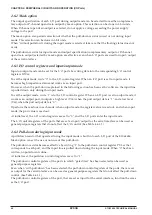
The clock timer can cause interrupts at the falling edge of 32 Hz, 8 Hz, 2 Hz, 1 Hz and 16 Hz signals.
Software can set whether to mask any of these frequencies.
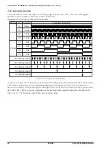
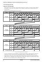
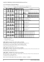
Figure 4.8.3.1 is the timing chart of the clock timer.

Address

FF75H

FF76H

32 Hz interrupt request

16 Hz interrupt request

8 Hz interrupt request

2 Hz interrupt request

1 Hz interrupt request

Bit

D0

D1

D2

D3

D0

D1

D2

D3

Frequency

Clock timer timing chart

128 Hz

64 Hz

32 Hz

16 Hz

8 Hz

4 Hz

2 Hz

1 Hz

Fig. 4.8.3.1  Timing chart of clock timer

As shown in Figure 4.8.3.1, interrupt is generated at the falling edge of the frequencies (32 Hz, 8 Hz, 2 Hz,
1 Hz, 16 Hz). At this time, the corresponding interrupt factor flag (IT0, IT1, IT2, IT3, IT4) is set to "1".
Selection of whether to mask the separate interrupts can be made with the interrupt mask registers (EIT0,
EIT1, EIT2, EIT3, EIT4). However, regardless of the interrupt mask register setting, the interrupt factor
flag is set to "1" at the falling edge of the corresponding signal.

Содержание S1C63656

Страница 1: ...Technical Manual CMOS 4 BIT SINGLE CHIP MICROCOMPUTER S1C63656 Technical Hardware S1C63656 ...

Страница 2: ...uiring high level reliability such as medical products Moreover no license to any intellectual property rights is granted by implication or otherwise and there is no representation or warranty that anything made in accordance with this material will be free from any patent or copyright infringement of a third party This material or portions thereof may contain technology or the subject relating to...

Страница 3: ...y Function Absolute Maximum Rating Recommended Operating Conditions DC Characteristics Diagram of Pad Layout Differences with the actual IC Contents Explanation was revised Explanation was revised Explanation was revised Table 2 2 2 1 was revised Table 4 1 1 e was revised Explanation was revised Explanation was revised Explanation was revised A note was added Explanation was revised Explanation wa...

Страница 4: ......

Страница 5: ...tion Package D die form F QFP B BGA Model number Model name C microcomputer digital products Product classification S1 semiconductor Development tools S5U1 C 63000 A1 1 Packing specifications 00 standard packing Version 1 Version 1 Tool type Hx ICE Ex EVA board Px Peripheral board Wx Flash ROM writer for the microcomputer Xx ROM writer peripheral board Cx C compiler package Ax Assembler package Dx...

Страница 6: ......
Страница 7: ...s at initial resetting 14 2 3 Test Terminal TEST 14 CHAPTER 3 CPU ROM RAM________________________________________ 15 3 1 CPU 15 3 2 Code ROM 15 3 3 RAM 15 3 4 Data ROM 16 CHAPTER 4 PERIPHERAL CIRCUITS AND OPERATION__________________________ 17 4 1 Memory Map 17 4 2 Watchdog Timer 26 4 2 1 Configuration of watchdog timer 26 4 2 2 Interrupt function 26 4 2 3 I O memory of watchdog timer 27 4 2 4 Pro...

Страница 8: ...nction 58 4 8 4 I O memory of clock timer 59 4 8 5 Programming notes 60 4 9 Stopwatch Timer 61 4 9 1 Configuration of stopwatch timer 61 4 9 2 Counter and prescaler 61 4 9 3 Capture buffer and hold function 62 4 9 4 Stopwatch timer RUN STOP and reset 63 4 9 5 Direct input function and key mask 63 4 9 6 Interrupt function 66 4 9 7 I O memory of stopwatch timer 68 4 9 8 Programming notes 71 4 10 Pro...

Страница 9: ...ng Motor Driver 121 4 15 1 Configuration of stepping motor driver 121 4 15 2 Setting up the motor drive pulse 122 4 15 3 Pulse output control 123 4 15 4 Interrupt function 123 4 15 5 I O memory of stepping motor driver 124 4 15 6 Programming notes 127 4 16 SVD Supply Voltage Detection Circuit 128 4 16 1 Configuration of SVD circuit 128 4 16 2 SVD operation 128 4 16 3 I O memory of SVD circuit 129 ...

Страница 10: ...155 9 1 Diagram of Pad Layout 155 9 2 Pad Coordinates 156 APPENDIX PERIPHERAL CIRCUIT BOARDS FOR S1C63656 ____________________ 157 A 1 Names and Functions of Each Part 157 A 1 1 S5U1C63000P1 157 A 1 2 S5U1C63658P2 160 A 2 Connecting to the Target System 161 A 3 Downloading to S5U1C63000P1 164 A 3 1 Downloading Circuit Data 1 when new ICE S5U1C63000H2 is used 164 A 3 2 Downloading Circuit Data 2 wh...

Страница 11: ...e to switch the 4 bits to serial I F input output 2 Serial interface 1 port 8 bit clock synchronous system LCD driver 38 segments 4 or 3 commons 2 Time base counter Clock timer Stopwatch timer 1 1000 sec with direct key input function Programmable timer 8 bit PWM 2 ch or 16 bit PWM 1 ch 2 Watchdog timer Built in Sound generator With envelope and 1 shot output functions R f converter 2 ch CR oscill...

Страница 12: ...REF1 RFIN0 RFIN1 RFOUT RESET P00 P03 P10 P13 R00 R03 BZ AO1 AO2 BO1 BO2 Core CPU S1C63000 ROM 6 144 words 13 bits System Reset Control Interrupt Generator OSC RAM 1 024 words 4 bits Data ROM 1 024 words 4 bits LCD Driver 38 SEG 4 COM Power Controller SVD Sound Generator Stepping Motor Driver Clock Timer Stopwatch Timer Programmable Timer Counter Input Port R f Converter Serial Interface I O Port O...

Страница 13: ... 140 141 142 143 144 Pin name CB VC1 VC2 VC3 VSSA RFOUT N C RFIN0 RFIN1 REF0 SEN0 REF1 SEN1 N C N C HUD N C N C N C N C N C VDDA VDDA VOSC N C N C N C N C OSC1 OSC2 VD1 N C OSC3 OSC4 VSS TEST Pin name RESET N C N C N C N C N C N C N C N C SEG19 SEG20 SEG21 SEG22 SEG23 SEG24 SEG25 SEG26 SEG27 SEG28 SEG29 SEG30 SEG31 SEG32 SEG33 SEG34 SEG35 SEG36 SEG37 N C N C N C N C N C N C COM2 COM3 Pin name VDD ...

Страница 14: ...tware I O port or serial I F ready signal output pin selected by software Output port pin Output port pin Output port or TOUT output pin selected by software Output port or FOUT output pin selected by software Motor driver Ch 1 drive pulse output pin 1 Motor driver Ch 1 drive pulse output pin 2 Motor driver Ch 2 drive pulse output pin 1 Motor driver Ch 2 drive pulse output pin 2 LCD common output ...

Страница 15: ...sed to select whether the pull down resistor working in the input mode is supplemented to the I O ports or not It is possible to select for each bit of the input ports Refer to Section 4 6 2 Mask option for details 6 Output specification of the output port Either complementary output or P channel open drain output can be selected as the output specifica tion for the output ports R00 R03 The select...

Страница 16: ...ica tions that meet the target system and check the appropriate box Be sure to record the specifications for unused functions too 1 OSC1 SYSTEM CLOCK 1 Crystal 2 OSC3 SYSTEM CLOCK 1 CR built in R 2 CR external R 3 Ceramic 4 No Operation disabled 3 INPUT PORT PULL DOWN RESISTOR K00 1 With Resistor 2 Gate Direct K01 1 With Resistor 2 Gate Direct K02 1 With Resistor 2 Gate Direct K03 1 With Resistor ...

Страница 17: ...entary 2 Pch OpenDrain 8 MULTIPLE KEY ENTRY RESET COMBINATION 1 Not Use 2 Use K00 K01 3 Use K00 K01 K02 4 Use K00 K01 K02 K03 9 MULTIPLE KEY ENTRY RESET TIME AUTHORIZE 1 Not Use 2 Use 10 SIO SYNC CLOCK SRDY 1 Negative 2 Positive 11 LCD DRIVING POWER 1 Internal Power 3 0 V panel normal mode with contrast adjustment function 2 External Power 1 3 bias VDD VC2 4 5 V panel 3 External Power 1 3 bias VDD...

Страница 18: ... C N SEG output S DC output C N SEG output S DC output C N SEG output S DC output C N SEG output S DC output C N SEG output S DC output C N SEG output S DC output C N SEG output S DC output C N SEG output S DC output C N SEG output S DC output C N SEG output S DC output C N SEG output S DC output C N SEG output S DC output C N SEG output S DC output C N SEG output S DC output C N SEG output S DC o...

Страница 19: ...it Voltage regulator for OSC1 oscillation circuit High speed operation voltage regulator LCD system voltage circuit Output voltage VOSC VOSC VD3 VC1 VC3 Note Do not drive external loads with the output voltage from the internal power supply circuits See Chapter 7 Electrical Characteristics for voltage values and drive capability External power supply LCD system voltage regulator LCD driver VDDA VD...

Страница 20: ...erates the LCD drive voltage This circuit allows the software to turn on and off Turn this circuit on before starting display on the LCD The LCD system voltage circuit generates VC1 with the voltage regulator built in and generates two other voltages VC2 2VC1 VC3 3VC1 by boosting VC1 The voltage regulator that generates VC1 provides two operating modes normal mode that allows adjustment of LCD con...

Страница 21: ...2 1 5 Analog system power supply The VDDA and VSSA power supply terminals are provided only for the R f converter in order to avoid decreasing the conversion accuracy due to noise However the same voltage level as the VDD VSS must be supplied to the VDDA VSSA VDDA VDD VSSA VSS ...

Страница 22: ...that the initial reset is released by setting the reset terminal to a low level VSS and the CPU starts operation The reset input signal is maintained by the RS latch and becomes the internal initial reset signal The RS latch is designed to be released by a 2 Hz signal high that is divided by the OSC1 clock Therefore in normal operation a maximum of 250 msec when fOSC1 32 768 kHz is needed until th...

Страница 23: ...1 Stack pointer SP2 Zero flag Carry flag Interrupt flag Extension flag Queue register CPU core Symbol A B EXT X Y PC SP1 SP2 Z C I E Q Number of bits 4 4 8 16 16 16 8 8 1 1 1 1 16 Setting value Undefined Undefined Undefined Undefined Undefined 0110H Undefined Undefined Undefined Undefined 0 0 Undefined Name RAM Display memory Other peripheral circuits Peripheral circuits Number of bits 4 4 Setting...

Страница 24: ...ws the list of the shared terminal settings Table 2 2 4 1 List of shared terminal settings Terminal name R00 R01 R02 R03 P00 P03 P10 P11 P12 P13 Terminal status at initial reset R00 LOW output R01 LOW output R02 LOW output R03 LOW output P00 P03 Input pulled down P10 Input pulled down P11 Input pulled down P12 Input pulled down P13 Input pulled down Special output TOUT FOUT TOUT FOUT Serial I F Wh...

Страница 25: ...s 0000H to 03FFH on the data memory map Addresses 0100H to 01FFH are 4 bit 16 bit data accessible areas and in other areas it is only possible to access 4 bit data When programming keep the following points in mind 1 Part of the RAM area is used as a stack area for subroutine call and register evacuation so pay attention not to overlap the data area and stack area 2 The S1C63000 core CPU handles t...

Страница 26: ...bit data 0000H 00FFH 0100H 01FFH 0200H 03FFH 4 bits 4 bit access area SP2 stack area 4 bit access area Data area 4 16 bit access area SP1 stack area Fig 3 3 1 Configuration of data RAM 3 4 Data ROM The data ROM is a mask ROM for loading various static data such as a character generator and has a capacity of 1 024 words 4 bits The data ROM is assigned to addresses 8000H to 83FFH on the data memory ...

Страница 27: ...word data ROM 48 word display memory and 101 word peripheral I O memory Figure 4 1 1 shows the overall memory map of the S1C63656 and Table 4 1 1 the peripheral circuits I O space memory maps 0000H 0400H 8000H 8400H F000H FF00H FFFFH RAM area Unused area Unused area Data ROM area I O memory area Display memory area Unused area Peripheral I O area F000H F030H FF00H FFFFH Fig 4 1 1 Memory map Note M...

Страница 28: ...d Motor driver Ch 1 pulse width selection FF10H 0 0 FTRG2 FRUN2 FTRG1 FRUN1 W R W R R 0 3 0 3 FTRG2 FRUN2 FTRG1 FRUN1 2 2 2 0 2 0 Trigger Run Trigger Run Invalid Stop Invalid Stop Unused Unused Motor driver Ch 2 trigger writing Motor driver Ch 2 status reading Motor driver Ch 1 trigger writing Motor driver Ch 1 status reading FF12H PFWA3 PFWA2 PFWA1 PFWA0 R W PFWA3 PFWA2 PFWA1 PFWA0 0 0 0 0 FF13H ...

Страница 29: ...ata K13 FF40H IOC03 IOC02 IOC01 IOC00 R W IOC03 IOC02 IOC01 IOC00 0 0 0 0 Output Output Output Output Input Input Input Input P00 P03 I O control register FF41H PUL03 PUL02 PUL01 PUL00 R W PUL03 PUL02 PUL01 PUL00 1 1 1 1 On On On On Off Off Off Off P00 P03 pull down control register FF42H P03 P02 P01 P00 R W P03 P02 P01 P00 2 2 2 2 High High High High Low Low Low Low P00 P03 I O port data FF44H IO...

Страница 30: ...et On Enable 0 5 sec Invalid Off Disable Envelope releasing time selection Envelope reset writing Envelope On Off Buzzer output enable FF6DH 0 BZSTP BZSHT SHTPW R W R W 0 3 BZSTP 3 BZSHT SHTPW 2 0 0 0 Stop Trigger Busy 125 msec Invalid Invalid Ready 31 25 msec Unused 1 shot buzzer stop writing 1 shot buzzer trigger writing 1 shot buzzer status reading 1 shot buzzer pulse width setting 0 4096 0 1 3...

Страница 31: ... 3 0 0 0 Reset Request Renewal Run Reset No No Stop Invalid Lap data carry up request flag Capture renewal flag Stopwatch timer Run Stop Stopwatch timer reset writing DRL3 DRL2 DRL1 DRL0 2 2 2 2 Low order 8 bit destination register low order 4 bits LSB R W FF82H DRL3 DRL2 DRL1 DRL0 DRL7 DRL6 DRL5 DRL4 2 2 2 2 MSB Low order 8 bit destination register high order 4 bits R W FF83H DRL7 DRL6 DRL5 DRL4 ...

Страница 32: ...ent counter mode Timer 0 pulse polarity selection for event counter mode R W FFC0H MOD16 EVCNT FCSEL PLPOL TC11 TC10 TC9 TC8 2 2 2 2 Time base counter TC8 TC11 R W FF99H TC11 TC10 TC9 TC8 TC15 TC14 TC13 TC12 2 2 2 2 Time base counter TC12 TC15 R W FF9AH TC15 TC14 TC13 TC12 TC19 TC18 TC17 TC16 2 2 2 2 MSB Time base counter TC16 TC19 R W FF9BH TC19 TC18 TC17 TC16 MC19 MC18 MC17 MC16 2 2 2 2 MSB Meas...

Страница 33: ...0 0 0 0 0 MSB Programmable timer 0 reload data low order 4 bits LSB R W FFC6H RLD03 RLD02 RLD01 RLD00 RLD07 RLD06 RLD05 RLD04 0 0 0 0 MSB Programmable timer 0 reload data high order 4 bits LSB R W FFC7H RLD07 RLD06 RLD05 RLD04 RLD13 RLD12 RLD11 RLD10 0 0 0 0 MSB Programmable timer 1 reload data low order 4 bits LSB R W FFC8H RLD13 RLD12 RLD11 RLD10 RLD17 RLD16 RLD15 RLD14 0 0 0 0 MSB Programmable ...

Страница 34: ...SMD1 R R W 0 3 0 3 EISMD2 EISMD1 2 2 0 0 Enable Enable Mask Mask Unused Unused Interrupt mask register Motor driver Ch 2 Interrupt mask register Motor driver Ch 1 FFD8H 0 0 PTSEL1 PTSEL0 R R W 0 3 0 3 PTSEL1 PTSEL0 2 2 0 0 PWM PWM Normal Normal Unused Unused Programmable timer 1 PWM output selection Programmable timer 0 PWM output selection FFE0H 0 0 ECTC1 ECTC0 R R W 0 3 0 3 ECTC1 ECTC0 2 2 0 0 E...

Страница 35: ...M R R W 0 3 0 3 IRFB IRFM 2 2 0 0 R Yes W Reset R No W Invalid Unused Unused Interrupt factor flag R f converter reference oscillate completion Interrupt factor flag R f converter sensor oscillate completion FFF8H 0 0 ISMD2 ISMD1 R R W 0 3 0 3 ISMD2 ISMD1 2 2 0 0 R Yes W Reset R No W Invalid Unused Unused Interrupt factor flag Motor driver Ch 2 Interrupt factor flag Motor driver Ch 1 IT3 IT2 IT1 I...

Страница 36: ... bit binary counter and generates the non maskable interrupt when the last stage of the counter 0 25 Hz overflows Watchdog timer reset processing in the program s main routine enables detection of program overrun such as when the main routine s watchdog timer processing is bypassed Ordinarily this routine is incorporated where periodic processing takes place just as for the timer interrupt routine...

Страница 37: ...hen 0 is written Disabled Reading Valid When 1 is written to the WDEN register the watchdog timer starts count operation When 0 is written the watchdog timer does not count and does not generate the interrupt NMI At initial reset this register is set to 1 WDRST Watchdog timer reset FF07H D0 Resets the watchdog timer When 1 is written Watchdog timer is reset When 0 is written No operation Reading A...

Страница 38: ...agram of this oscillation system VOSC VD1 High speed operation voltage regulator Voltage regulator for OSC1 oscillation circuit Oscillation circuit control signal CPU clock selection signal To CPU To peripheral circuits Clock switch OSC3 oscillation circuit OSC1 oscillation circuit Divider Mask option Fig 4 3 1 1 Oscillation system block diagram 4 3 2 OSC1 oscillation circuit The OSC1 crystal osci...

Страница 39: ...scillation circuit CCR R CR VSS CGC CDC Ceramic OSC4 OSC3 R RDC To CPU and some peripheral circuits Oscillation circuit control signal FC To CPU and some peripheral circuits Oscillation circuit control signal a CR oscillation circuit external R type CCR OSC3 OSC4 R CR Fig 4 3 3 1 OSC3 oscillation circuit As shown in Figure 4 3 3 1 the CR oscillation circuit external R type can be configured simply...

Страница 40: ...tion clock from OSC1 to OSC3 do this after a minimum of 5 msec have elapsed since the OSC3 oscillation went on Further the oscillation stabilization time varies depending on the external oscillator characteristics and conditions of use so allow ample margin when setting the wait time OSC3 OSC1 1 Set CLKCHG to 0 CPU clock OSC3 OSC1 2 Set OSCC to 0 OSC3 oscillation on off Note When switching the clo...

Страница 41: ...Initial value at initial reset 2 Not set in the circuit 3 Constantly 0 when being read OSCC OSC3 oscillation control register FF01H D2 Turns the OSC3 oscillation circuit on and off When 1 is written OSC3 oscillation On When 0 is written OSC3 oscillation Off Reading Valid When it is necessary to operate the CPU at high speed set OSCC to 1 At other times set it to 0 to reduce current consumption At ...

Страница 42: ...he OSC3 oscillation went on Further the oscillation stabilization time varies depending on the external oscillator characteristics and conditions of use so allow ample margin when setting the wait time 2 When switching the clock form OSC3 to OSC1 use a separate instruction for switching the OSC3 oscillation off An error in the CPU operation can result if this processing is performed at the same ti...

Страница 43: ... for slide switch input and interfacing with other LSIs The K00 and K01 input ports can also be used as the Run Stop and Lap direct inputs for the stopwatch timer and the K13 port can also be used as the event counter input for the programmable timer 4 4 2 Interrupt function All eight bits of the input ports K00 K03 K10 K13 provide the interrupt function The conditions for issuing an interrupt can...

Страница 44: ...of an interrupt for K00 K03 Interrupt selection register SIK03 1 SIK02 1 SIK01 1 SIK00 0 Input port 1 Initial value Interrupt generation K03 1 K02 0 K01 1 K00 0 Input comparison register KCP03 1 KCP02 0 KCP01 1 KCP00 0 With the above setting the interrupt of K00 K03 is generated under the following condition 2 K03 1 K02 0 K01 1 K00 1 3 K03 0 K02 0 K01 1 K00 1 4 K03 0 K02 1 K01 1 K00 1 Because K00 ...

Страница 45: ... K10 K13 input port data FF26H KCP13 KCP12 KCP11 KCP10 R W KCP13 KCP12 KCP11 KCP10 1 1 1 1 K10 K13 input comparison register FFE3H 0 0 0 EIK0 R R W 0 3 0 3 0 3 EIK0 2 2 2 0 Enable Mask Unused Unused Unused Interrupt mask register K00 K03 FFE4H 0 0 0 EIK1 R R W 0 3 0 3 0 3 EIK1 2 2 2 0 Enable Mask Unused Unused Unused Interrupt mask register K10 K13 FFF3H 0 0 0 IK0 R R W 0 3 0 3 0 3 IK0 2 2 2 0 R Y...

Страница 46: ...gisters At initial reset these registers are set to 1 EIK0 K0 input interrupt mask register FFE3H D0 EIK1 K1 input interrupt mask register FFE4H D0 Masking the interrupt of the input port can be selected with these registers When 1 is written Enable When 0 is written Mask Reading Valid With these registers masking of the input port interrupt can be selected for each of the two systems K00 K03 K10 ...

Страница 47: ...are needs to be taken of the key scan during key matrix configuration Make this waiting time the amount of time or more calculated by the following expression 10 C R C terminal capacitance 5 pF parasitic capacitance pF R pull down resistance 375 kΩ Max 2 After an interrupt occurs the same interrupt will occur again if the interrupt enabled state I flag 1 is set or the RETI instruction is executed ...

Страница 48: ...n is selected by the software At initial reset these are all set to the general purpose output port Table 4 5 1 1 shows the setting of the output terminals by function selection Table 4 5 1 1 Function setting of output terminals Terminal name R00 R01 R02 R03 Terminal status at initial reset R00 Low output R01 Low output R02 Low output R03 Low output Special output TOUT FOUT R00 R00 R01 R01 TOUT FO...

Страница 49: ...onfiguration of the R02 and R03 output ports Table 4 5 4 1 Special output Terminal R03 R02 Special output FOUT TOUT Output control register FOUTE PTOUT Data bus Register PTOUT Register R02 TOUT R02 TOUT Register FOUTE Register R03 Register R03HIZ Register R02HIZ FOUT R03 FOUT Fig 4 5 4 1 Configuration of R02 and R03 output ports At initial reset the output port data register is set to 0 and the hi...

Страница 50: ...rnal circuit and can be used to provide a clock signal to an external device To output the FOUT signal fix the R03 register at 1 and the R03HIZ register at 0 and turn the signal on and off using the FOUTE register The frequency of the output clock may be selected from among 4 types shown in Table 4 5 4 2 by setting the FOFQ0 and FOFQ1 registers Table 4 5 4 2 FOUT clock frequency FOFQ1 1 1 0 0 FOFQ...

Страница 51: ...ed TOUT output selection TOUT output control R R W FFC1H 0 0 CHSEL0 PTOUT 1 Initial value at initial reset 2 Not set in the circuit 3 Constantly 0 when being read R00HIZ R03HIZ R0 port high impedance control register FF30H Controls high impedance output of the output port When 1 is written High impedance When 0 is written Data output Reading Valid By writing 0 to the high impedance control registe...

Страница 52: ...en TOUT output Off Reading Valid By writing 1 to the PTOUT register when the R02 register has been set to 1 and the R02HIZ register has been set to 0 the TOUT signal is output from the R02 terminal When 0 is written the R02 termi nal goes high VDD When using the R02 output port for DC output fix this register at 0 At initial reset this register is set to 0 4 5 6 Programming notes 1 When using the ...

Страница 53: ...e terminals are all set to the I O port Table 4 6 1 1 shows the setting of the input output terminals by function selection Table 4 6 1 1 Function setting of input output terminals Terminal P00 P03 P10 P11 P12 P13 Terminal status at initial reset P00 P03 Input pull down P10 Input pull down P11 Input pull down P12 Input pull down P13 Input pull down Serial I F Master P00 P03 SIN I SOUT O SCLK O P13...

Страница 54: ...rite 1 is to the I O control register When an I O port is set to output mode it works as an output port it outputs a high level VDD when the port output data is 1 and a low level VSS when the port output data is 0 If perform the read out in each mode when output mode the register value is read out and when input mode the port value is read out At initial reset the I O control registers are set to ...

Страница 55: ...er ESIF 0 functions as a general purpose register when SIF is selected P11 I O control register ESIF 0 functions as a general purpose register when SIF is selected P10 I O control register ESIF 0 functions as a general purpose register when SIF is selected FF45H PUL13 PUL12 PUL11 PUL10 R W PUL13 PUL12 PUL11 PUL10 1 1 1 1 On On On On Off Off Off Off P13 pull down control register functions as a gen...

Страница 56: ...written as the port data the port terminal goes high VDD and when 0 is written the terminal goes low VSS Port data can be written also in the input mode When reading data When 1 is read High level When 0 is read Low level The terminal voltage level of the I O port is read out When the I O port is in the input mode the voltage level being input to the port terminal can be read out in the output mod...

Страница 57: ...to enable in 1 bit units The pull down resistor is included into the ports selected by mask option By writing 1 to the pull down control register the corresponding I O ports are pulled down during input mode while writing 0 disables the pull down function At initial reset these registers are all set to 1 so the pull down function is enabled The pull down control registers of the ports in which the...

Страница 58: ...1 3 bias for 3 0 V panel VDD VC3 3 External power supply 1 2 bias for 3 0 V panel VDD VC3 VC1 VC2 static drive function is available Note that the power control using the LPWR register is necessary even if an external power supply is used SEG output ports that are set for DC output by the mask option operate same as the output R port regardless of the power on off control by the LPWR register 4 7 ...

Страница 59: ...HAPTER 4 PERIPHERAL CIRCUITS AND OPERATION LCD Driver COM0 COM1 COM2 COM3 SEG0 SEG37 VC3 VC2 VC1 VSS VC3 VC2 VC1 VSS VC2 VC1 Not lit Lit LCD lighting status COM0 COM1 COM2 COM3 SEG0 37 Frame Fig 4 7 3 1 Dynamic drive waveform for 1 4 duty ...

Страница 60: ...PTER 4 PERIPHERAL CIRCUITS AND OPERATION LCD Driver COM0 COM1 COM2 COM3 SEG0 SEG37 VC3 VC2 VC1 VSS VC3 VC2 VC1 VSS VC2 VC1 VC2 VC1 Not lit Lit LCD lighting status COM0 COM1 COM2 SEG0 37 Frame Fig 4 7 3 2 Dynamic drive waveform for 1 3 duty ...

Страница 61: ...ng to the SEG terminal the SEG terminal outputs a static on waveform When all the COM0 to COM3 bits are set to 0 the SEG terminal outputs a dynamic off waveform Figure 4 7 3 3 shows the static drive waveform COM 0 3 Frame frequency VC3 VC2 VC1 VSS VC3 VC2 VC1 VSS VC3 VC2 VC1 VSS SEG 0 37 LCD lighting status COM0 COM1 COM2 COM3 SEG0 37 Not lit Lit Fig 4 7 3 3 Static drive waveform Note To use the s...

Страница 62: ...t This makes design easy by increasing the degree of freedom with which the liquid crystal panel can be designed Figure 4 7 5 1 shows an example of the relationship between the LCD segments on the panel and the display memory for the case of 1 4 duty a f g e d p c SEG10 SEG11 Common 0 Common 1 Common 2 F020H F021H Address d p D3 c g D2 b f D1 a e D0 Data Display memory allocation SEG10 SEG11 21 D1...

Страница 63: ...G output S DC output C N SEG output S DC output C N SEG output S DC output C N SEG output S DC output C N SEG output S DC output C N SEG output S DC output C N SEG output S DC output C N SEG output S DC output C N SEG output S DC output C N SEG output S DC output C N SEG output S DC output C N SEG output S DC output C N SEG output S DC output C N SEG output S DC output C N SEG output S DC output C...

Страница 64: ...6 1 LCD contrast No 0 1 2 3 4 5 6 7 8 9 10 11 12 13 14 15 LC3 0 0 0 0 0 0 0 0 1 1 1 1 1 1 1 1 LC2 0 0 0 0 1 1 1 1 0 0 0 0 1 1 1 1 LC1 0 0 1 1 0 0 1 1 0 0 1 1 0 0 1 1 LC0 0 1 0 1 0 1 0 1 0 1 0 1 0 1 0 1 VC1 V 1 03 1 06 1 09 1 12 1 15 1 18 1 20 1 23 1 26 1 28 1 30 1 32 1 34 1 36 1 38 1 40 Contrast light dark At initial reset the LC0 LC3 are set to 0000B The software should initialize the register to...

Страница 65: ...being read Address Base Low 0 1 2 3 4 5 6 7 8 9 A B C D E F F000H F010H F020H Display memory 48 words 4 bits R W Fig 4 7 7 1 Display memory map LPWR LCD power control on off register FF60H D0 Turns the LCD system voltage circuit on and off When 1 is written On When 0 is written Off Reading Valid When 1 is written to the LPWR register the LCD system voltage circuit goes on and generates the LCD dri...

Страница 66: ... segments fade out When 0 is written Normal display Reading Valid By writing 1 to the ALOFF register all the LCD segments go off and when 0 is written it returns to normal display This function outputs an off waveform to the SEG terminals and does not affect the content of the display memory ALON FF61H D1 has priority over ALOFF so all the LCD segments go on when ALON and ALOFF are set to 1 simult...

Страница 67: ...H D0 TM0 128 Hz D1 TM1 64 Hz D2 TM2 32 Hz D3 TM3 16 Hz FF76H D0 TM4 8 Hz D1 TM5 4 Hz D2 TM6 2 Hz D3 TM7 1 Hz Since the clock timer data has been allocated to two addresses a carry is generated from the low order data within the count TM0 TM3 128 16 Hz to the high order data TM4 TM7 8 1 Hz When this carry is generated between the reading of the low order data and the high order data a content combi...

Страница 68: ...t 1 Hz interrupt request Bit D0 D1 D2 D3 D0 D1 D2 D3 Frequency Clock timer timing chart 128 Hz 64 Hz 32 Hz 16 Hz 8 Hz 4 Hz 2 Hz 1 Hz Fig 4 8 3 1 Timing chart of clock timer As shown in Figure 4 8 3 1 interrupt is generated at the falling edge of the frequencies 32 Hz 8 Hz 2 Hz 1 Hz 16 Hz At this time the corresponding interrupt factor flag IT0 IT1 IT2 IT3 IT4 is set to 1 Selection of whether to ma...

Страница 69: ...factor flag Clock timer 1 Hz Interrupt factor flag Clock timer 2 Hz Interrupt factor flag Clock timer 8 Hz Interrupt factor flag Clock timer 32 Hz FFE9H 0 0 0 EIT4 R R W 0 3 0 3 0 3 EIT4 2 2 2 0 Enable Mask Unused Unused Unused Interrupt mask register Clock timer 16 Hz FFF9H 0 0 0 IT4 R R W 0 3 0 3 0 3 IT4 2 2 2 0 R Yes W Reset R No W Invalid Unused Unused Unused Interrupt factor flag Clock timer ...

Страница 70: ... FFF5H D2 IT3 1 Hz interrupt factor flag FFF5H D3 IT4 16 Hz interrupt factor flag FFF9H D0 These flags indicate the status of the clock timer interrupt When 1 is read Interrupt has occurred When 0 is read Interrupt has not occurred When 1 is written Flag is reset When 0 is written Invalid The interrupt factor flags IT0 IT1 IT2 IT3 IT4 correspond to the clock timer interrupts of the respective freq...

Страница 71: ...rate timer from the clock timer In particular digital watch stopwatch functions can be realized easily with software 4 9 2 Counter and prescaler The stopwatch timer is configured of four bit BCD counters SWD0 3 SWD4 7 and SWD8 11 The counter SWD0 3 at the stage preceding the stopwatch timer has a 1 000 Hz signal generated by the prescaler for the input clock It counts up every 1 1 000 sec and gene...

Страница 72: ...eased when SWD8 11 1 10 sec reading is completed Therefore data should be read in order of SWD0 3 SWD4 7 SWD8 11 If SWD4 7 or SWD8 11 is first read when data have not been held the hold function does not work and data in the counter is directly read out When data that has not been held is read in the stopwatch timer RUN status you cannot judge whether it is correct or not The stopwatch timer has a...

Страница 73: ...nd is maintained as is When the stopwatch timer is reset in the RUN status counting restarts from count 000 Also in the STOP status the reset data 000 is maintained until the next RUN 4 9 5 Direct input function and key mask The stopwatch timer has a direct input function that can control the RUN STOP and LAP operation of the stopwatch timer by external key input This function is set by writing 1 ...

Страница 74: ...newal flag is set renewed data is held in the capture buffer So it is necessary to read from SWD0 3 again The stopwatch timer sets the 1 Hz interrupt factor flag ISW1 to 1 when requiring a carry up to 1 sec digit by an SWD8 11 overflow If the capture buffer shifts into hold status when SWD0 3 is read or when LAP is input while the 1 Hz interrupt factor flag ISW1 is set to 1 the lap data carry up r...

Страница 75: ...or LAP inputs become invalid in the following status 1 The RUN or LAP key is pressed when one or more keys that are included in the selected combina tion here in after referred to as mask are held down 2 The RUN or LAP key has been pressed when the mask is released fOSC1 32 1 024 Hz Direct RUN LAP input Key mask valid invalid invalid invalid Fig 4 9 5 4 Operation of key mask RUN or LAP inputs beco...

Страница 76: ...D3 D0 D1 D2 D3 Address Register Stopwatch timer SWD0 3 timing chart FF7AH 1 1 000 sec BCD D0 D1 D2 D3 Address Register Stopwatch timer SWD4 7 timing chart Address Register Stopwatch timer SWD8 11 timing chart Fig 4 9 6 1 Timing chart for counters As shown in Figure 4 9 6 1 the interrupts are generated by the overflow of their respective counters 9 changing to 0 Also at this time the corresponding ...

Страница 77: ...LAP The direct RUN and LAP functions use the K00 and K01 ports Therefore the direct input interrupt and the K00 K03 inputs interrupt may generate at the same time depending on the interrupt condi tion setting for the input port K00 K03 Consequently when using the direct input interrupt set the interrupt selection registers SIK00 and SIK01 to 0 so that the input interrupt does not generate by K00 a...

Страница 78: ...riting FFE6H EIRUN EILAP EISW1 EISW10 R W EIRUN EILAP EISW1 EISW10 0 0 0 0 Enable Enable Enable Enable Mask Mask Mask Mask Interrupt mask register Stopwatch direct RUN Interrupt mask register Stopwatch direct LAP Interrupt mask register Stopwatch timer 1 Hz Interrupt mask register Stopwatch timer 10 Hz FFF6H IRUN ILAP ISW1 ISW10 R W IRUN ILAP ISW1 ISW10 0 0 0 0 R Yes W Reset R No W Invalid Interru...

Страница 79: ...tatuses are input to the stopwatch timer as the RUN STOP and LAP inputs according to this selection At initial reset this register is set to 0 DKM0 DKM2 Direct key mask selection register FF78H D0 D2 Selects a combination of the key inputs for concurrence judgment with RUN and LAP inputs when the direct input function is set Table 4 9 7 2 Key mask selection DKM2 0 0 0 0 1 1 1 1 DKM1 0 0 1 1 0 0 1 ...

Страница 80: ...t required Writing Invalid If the capture buffer shifts into hold status while the 1 Hz interrupt factor flag ISW1 is set to 1 LCURF is set to 1 to indicate that a carry up to 1 sec digit is required When performing a processing such as a LAP input preceding with 1 Hz interrupt processing read this flag before processing and check whether carry up is needed or not This flag is renewed set reset ev...

Страница 81: ...rupt factor flag is reset Therefore be sure to reset write 1 to the interrupt factor flag in the interrupt service routine before shifting to the interrupt enabled state At initial reset these flags are set to 0 4 9 8 Programming notes 1 The interrupt factor flag should be reset after resetting the stopwatch timer 2 Be sure to data reading in the order of SWD0 3 SWD4 7 SWD8 11 3 When data that is ...

Страница 82: ...compare match signal if the contents between the down counter and the compare data register are matched and an interrupt occurs at the same time Also the compare match signal is used with the underflow signal to generate a PWM waveform The signal generated by the programmable timer can be output from the R02 output port terminal Interrupt request CHSEL0 TOUT R02 Serial interface Interrupt control ...

Страница 83: ...s counting This control RUN STOP does not affect the counter data The counter maintains its data while stopped and can restart counting continuing from that data The counter data can be read via the data buffer PTDx0 PTDx7 in optional timing However the counter has the data hold function the same as the clock timer that holds the high order data PTDx4 PTDx7 when the low order data PTDx0 PTDx3 is r...

Страница 84: ...ection of prescaler division ratio Select the division ratio for each prescaler from among 4 types This selection is done using the prescaler division ratio selection register PTPSx0 PTPSx1 Table 4 10 3 1 shows the correspondence between the setting value and the division ratio Table 4 10 3 1 Selection of prescaler division ratio PTPSx1 1 1 0 0 PTPSx0 1 0 1 0 Prescaler division ratio Source clock ...

Страница 85: ...aveform When using this function write 1 to the PTSEL0 register for timer 0 or PTSEL1 register for timer 1 to set the timer in the PWM mode The compare data register CDx0 CDx7 x represents a timer number is provided for timers 0 and 1 to control the PWM waveform When the timer is set in the PWM mode the timer compares data between the down counter and the compare data register and outputs the comp...

Страница 86: ...uration of 16 bit timer The registers for timer 0 are used to control the timer The event counter and PWM output functions can also be used Timer 1 operates with the timer 0 underflow signal as the count clock so the clock and RUN STOP control registers for timer 1 become invalid However reload data PTRSTx must be preset to timers 0 and 1 separately The counter data in 16 bit mode must be read in ...

Страница 87: ...rom the R02 output port terminal Figure 4 10 8 1 shows the configuration of the output port R02 Data bus Register PTOUT Register R02 TOUT R02 TOUT Register R02HIZ Fig 4 10 8 1 Configuration of R02 The output of a TOUT signal is controlled by the PTOUT register When 1 is written to the PTOUT register the TOUT signal is output from the R02 output port terminal and when 0 is written the terminal goes...

Страница 88: ... timer 1 into RUN state PTRUN1 1 It is not necessary to control with the PTOUT register PTRUN1 Timer 1 underflow Source clock for serial I F Fig 4 10 9 1 Synchronous clock of serial interface A setting value for the RLD1x register according to a transfer rate is calculated by the following expres sion RLD1x fosc 2 bps division ratio of the prescaler 1 fosc Oscillation frequency OSC1 OSC3 bps Trans...

Страница 89: ... RLD03 RLD02 RLD01 RLD00 RLD07 RLD06 RLD05 RLD04 0 0 0 0 MSB Programmable timer 0 reload data high order 4 bits LSB R W FFC7H RLD07 RLD06 RLD05 RLD04 RLD13 RLD12 RLD11 RLD10 0 0 0 0 MSB Programmable timer 1 reload data low order 4 bits LSB R W FFC8H RLD13 RLD12 RLD11 RLD10 RLD17 RLD16 RLD15 RLD14 0 0 0 0 MSB Programmable timer 1 reload data high order 4 bits LSB R W FFC9H RLD17 RLD16 RLD15 RLD14 P...

Страница 90: ... selection FFF1H 0 0 IPT1 IPT0 R R W 0 3 0 3 IPT1 IPT0 2 2 0 0 R Yes W Reset R No W Invalid Unused Unused Interrupt factor flag Programmable timer 1 underflow Interrupt factor flag Programmable timer 0 underflow FFE1H 0 0 EIPT1 EIPT0 R R W 0 3 0 3 EIPT1 EIPT0 2 2 0 0 Enable Enable Mask Mask Unused Unused Interrupt mask register Programmable timer 1 underflow Interrupt mask register Programmable ti...

Страница 91: ... is set to 0 EVCNT Timer 0 counter mode selection register FFC0H D2 Selects a counter mode for timer 0 When 1 is written Event counter mode When 0 is written Timer mode Reading Valid The counter mode for timer 0 is selected from either the event counter mode or timer mode When 1 is written to the EVCNT register the event counter mode is selected and when 0 is written the timer mode is selected At ...

Страница 92: ...et to 0 RLD00 RLD07 Timer 0 reload data register FFC6H FFC7H RLD10 RLD17 Timer 1 reload data register FFC8H FFC9H Sets the initial value for the counter The reload data written in this register is loaded to the respective counters The counter counts down using the data as the initial value for counting Reload data is loaded to the counter when the counter is reset by writing 1 to the PTRSTx regist...

Страница 93: ...intained until the counter is reset or is set in the next RUN status When STOP status changes to RUN status the data that has been maintained can be used for resuming the count At initial reset these registers are set to 0 CHSEL0 TOUT output channel selection register FFC1H D1 Selects the channel used for TOUT signal output When 1 is written Timer 1 When 0 is written Timer 0 Reading Valid This reg...

Страница 94: ...red When 1 is written Flag is reset When 0 is written Invalid IPTx and ICTCx are the interrupt factor flags that respectively correspond to the interrupts for counter underflow and compare match and are set to 1 by generation of each factor The underflow interrupt factor is generated at the point where the counter underflows The compare match interrupt factor is generated if the counter data and t...

Страница 95: ...d 1 The PTRUNx register maintains 1 for reading until the timer actually stops Figure 4 10 11 1 shows the timing chart for the RUN STOP control PTRUNx WR PTDx0 PTDx7 42H 41H 40H 3FH 3EH 3DH PTRUNx RD Input clock 1 RUN writing 0 STOP writing Fig 4 10 11 1 Timing chart for RUN STOP control It is the same even in the event counter mode Therefore be aware that the counter does not enter RUN STOP statu...

Страница 96: ...ad data to the counter and the counter data is determined at the next rising edge of the input clock period shown in as in the figure Input clock Counter data continuous mode Reload data 25H 03H 02H 01H 00H 25H 24H Counter data is determined by reloading Underflow interrupt is generated Fig 4 10 11 2 Reload timing for programmable timer To avoid improper reloading do not rewrite the reload data af...

Страница 97: ...nal which indicates whether or not the serial interface is available to transmit or receive can be output to the SRDY terminal SD0 SD7 SIN P10 SCLK or SCLK P12 SCS0 SCS1 Output latch Serial I F interrupt control circuit Interrupt request SOUT P11 SRDY or SRDY P13 SCTRG Serial I F activating circuit fOSC1 Serial clock counter Serial clock selector Serial clock generator Shift register 8 bits Progra...

Страница 98: ... is assumed that positive polarity SCLK SRDY has been selected 4 11 3 Master mode and slave mode of serial interface The serial interface of the S1C63656 has two types of operation mode master mode and slave mode The master mode uses an internal clock as the synchronous clock for the built in shift register and outputs this internal clock from the SCLK P12 terminal to control the external slave si...

Страница 99: ...3H and writing 1 to SCTRG bit FF70H D1 it synchronizes with the synchronous clock and the serial data is output to the SOUT P11 terminal The synchronous clock used here is as follows in the master mode internal clock which is output to the SCLK P12 terminal while in the slave mode external clock which is input from the SCLK P12 terminal Shift timing of serial data is as follows When positive polar...

Страница 100: ...0 SD7 by software Serial data input output permutation The S1C63656 allows the input output permutation of serial data to be selected by the SDP register FF71H D3 as to either LSB first or MSB first The block diagram showing input output permutation in case of LSB first and MSB first is provided in Figure 4 11 4 1 The SDP register should be set before setting data to SD0 SD7 SIN SIN Address FF73H ...

Страница 101: ...e mode SCTRG W SCTRG R SCLK SIN 8 bit shift register SOUT ISIF SRDY Slave mode b When SCPS 0 Fig 4 11 4 2 Serial interface timing chart when synchronous clock is positive polarity SCLK SCTRG W SCTRG R SCLK SIN 8 bit shift register SOUT ISIF SRDY Slave mode SCTRG W SCTRG R SCLK SIN 8 bit shift register SOUT ISIF SRDY Slave mode b When SCPS 0 Fig 4 11 4 3 Serial interface timing chart when synchrono...

Страница 102: ...data high order 4 bits LSB SCS1 0 Clock SCS1 0 Clock FF71H SDP SCPS SCS1 SCS0 R W SDP SCPS SCS1 SCS0 0 0 0 0 MSB first LSB first Serial I F data input output permutation Serial I F clock phase selection Negative polarity mask option Positive polarity mask option Serial I F clock mode selection FF70H 0 ESOUT SCTRG ESIF R R W 0 3 ESOUT SCTRG ESIF 2 0 0 0 Enable Trigger Run SIF Disable Invalid Stop I...

Страница 103: ...n register FF71H D0 D1 Selects the synchronous clock SCLK for the serial interface Table 4 11 5 2 Synchronous clock selection SCS1 1 1 0 0 SCS0 1 0 1 0 Mode Master mode Slave mode Synchronous clock OSC1 OSC1 2 Programmable timer External clock The maximum clock is limited to 1 MHz Synchronous clock SCLK is selected from among the above 4 types 3 types of internal clock and external clock When the ...

Страница 104: ...o SCTRG The internal circuit of the serial interface is initiated through data writ ing reading on data registers SD0 SD7 In addition be sure to enable the serial interface with the ESIF register before setting the trigger Supply trigger only once every time the serial interface is placed in the RUN state Refrain from perform ing trigger input multiple times as leads to malfunctioning Moreover whe...

Страница 105: ...ETI instruction is executed unless the interrupt factor flag is reset Therefore be sure to reset write 1 to the interrupt factor flag in the interrupt service routine before shifting to the interrupt enabled state At initial reset this flag is set to 0 4 11 6 Programming notes 1 Perform data writing reading to the data registers SD0 SD7 only while the serial interface is not running i e the synchr...

Страница 106: ...und generator fOSC1 BZ terminal Programmable dividing circuit 256 Hz One shot buzzer control circuit Duty ratio control circuit BZFQ0 BZFQ2 BDTY0 BDTY2 Buzzer output control circuit Envelope addition circuit ENON BZE ENRTM ENRST BZSTP BZSHT SHTPW Fig 4 12 1 1 Configuration of sound generator 4 12 2 Control of buzzer output The BZ signal generated by the sound generator is output from the BZ termin...

Страница 107: ... 0 0 0 1 1 1 1 Level Level 1 Max Level 2 Level 3 Level 4 Level 5 Level 6 Level 7 Level 8 Min 4096 0 2048 0 8 16 7 16 6 16 5 16 4 16 3 16 2 16 1 16 3276 8 1638 4 8 20 7 20 6 20 5 20 4 20 3 20 2 20 1 20 2730 7 1365 3 12 24 11 24 10 24 9 24 8 24 7 24 6 24 5 24 2340 6 1170 3 12 28 11 28 10 28 9 28 8 28 7 28 6 28 5 28 Duty ratio by buzzer frequency Hz When the high level output time has been made TH an...

Страница 108: ...uated down to level 8 minimum it is retained at that level The duty ratio can be returned to maximum by writing 1 into register ENRST during output of a envelope attached buzzer signal The envelope attenuation time time for changing of the duty ratio can be selected by the register ENRTM The time for a 1 stage level change is 62 5 msec 16 Hz when 0 has been written into ENRTM and 125 msec 8 Hz whe...

Страница 109: ...T also permits reading When BZSHT is 1 the one shot output circuit is in operation during one shot output and when it is 0 it shows that the circuit is in the ready outputtable status In addition it can also terminate one shot output prior to the elapsing of the set time This is done by writing a 1 into the one shot buzzer stop BZSTP In this case as well the buzzer signal goes off in synchronizati...

Страница 110: ...BZSHT SHTPW R W R W 0 3 BZSTP 3 BZSHT SHTPW 2 0 0 0 Stop Trigger Busy 125 msec Invalid Invalid Ready 31 25 msec Unused 1 shot buzzer stop writing 1 shot buzzer trigger writing 1 shot buzzer status reading 1 shot buzzer pulse width setting 1 Initial value at initial reset 2 Not set in the circuit 3 Constantly 0 when being read BZE Buzzer output control register FF6CH D0 Controls the buzzer signal o...

Страница 111: ... No operation Reading Always 0 Writing 1 into ENRST resets envelope and the duty ratio becomes maximum If an envelope has not been added ENON 0 and if no buzzer signal is being output the reset becomes invalid Writing 0 is also invalid This bit is dedicated for writing and is always 0 for reading ENON Envelope On Off control register FF6CH D1 Controls the addition of an envelope onto the buzzer si...

Страница 112: ... When a re trigger is assigned during a one shot output the one shot output time set with SHTPW is measured again from that point time extension When reading When 1 is read BUSY When 0 is read READY During reading BZSHT shows the operation status of the one shot output circuit During one shot output BZSHT becomes 1 and the output goes off it shifts to 0 At initial reset this bit is set to 0 BZSTP ...

Страница 113: ...rm a multiplication set the multiplier to the source register SR and the multiplicand to the low order 8 bits DRL of the destination register then write 0 to the calculation mode selection register CALMD The multiplication takes 10 CPU clock cycles from writing 0 to CALMD until the 16 bit product is loaded into the destination register DRH and DRL At the same time the result is loaded the operatio...

Страница 114: ...ge Z flag Set when the 8 bit value in DRL is 00H and reset when it is not 00H Examples of division DRH DRL dividend SR divisor DRL quotient DRH remainder NF VF ZF 1A16H 64H 42H 4EH 0 0 0 332CH 64H 83H 00H 1 0 0 0000H 58H 00H 00H 0 0 1 2468H 13H 68H 24H 1 1 0 In the example of 2468H 13H shown above DRH DRL maintains the dividend because the quotient overflows the 8 bit To get the correct results wh...

Страница 115: ...shows a sample program ldb ext src_data h ldb xl src_data l Set RAM address for operand ldb ext au h ldb yl au l Set multiplier I O memory address ldb ba x ldb y ba Set data to SR ldb ba x ldb y ba Set data to DRL ldb ba x ldb y ba Set data to DRH ld y 0b0001 Start operation select calculation mode ldb ext rslt_data h ldb xl rslt_data l Set result store address nop nop nop Dummy instructions to wa...

Страница 116: ... DRH4 2 2 2 2 MSB High order 8 bit destination register high order 4 bits R W FF85H DRH7 DRH6 DRH5 DRH4 1 Initial value at initial reset 2 Not set in the circuit 3 Constantly 0 when being read SR0 SR7 Source register FF80H FF81H Used to set multipliers and divisors Set the low order 4 bits of data to SR0 SR3 and the high order 4 bits to SR4 SR7 This register maintains the latest set value until th...

Страница 117: ...al reset this flag is set to 0 VF Overflow flag FF86H D2 Indicates whether an overflow has occurred or not in a division process When 1 is read Overflow occurred When 0 is read Overflow has not occurred Writing Invalid When a multiplication process has finished this flag is always set to 0 VF is a read only bit so writing operation is invalid At initial reset this flag is set to 0 ZF Zero flag FF8...

Страница 118: ...nal reference resistance of the resistive sensor that has been connected to the sensor input terminal is converted into frequency by the CR oscillation circuit and the number of clocks is counted in the built in measurement counter By reading the value of the measure ment counter it can obtain the data after digitally converting the value detected by the sensor Various sensor circuits such as temp...

Страница 119: ...n using a normal resistive sensor DC bias such as temperature measurement using thermistor At initial reset channel 1 is set into this conversion method Figure 4 14 2 1 shows the connection diagram of external elements R1 R2 VSS C SEN0 REF0 RFIN0 Channel 0 R1 R2 VSS C SEN1 HUD REF1 RFIN1 Channel 1 R1 R2 C Thermistor Reference resistor Capacitor Fig 4 14 2 1 Connection diagram in case of R f conver...

Страница 120: ...tor becomes discharged and oscilla tion is performed according to CR time constant The time constant changes as the sensor resistance value fluctuates producing a difference from the oscillation frequency of the reference resistance Oscillation waveforms are shaped by the schmitt trigger and transmitted to the measurement counter The clock transmitted to the measurement counter is also output from...

Страница 121: ... of resistive humidity sensor Connect a humidity sensor between the HUD and SEN1 terminals and connect a reference resistance between the REF1 and RFIN1 terminals Connect an oscillating capacitor that is used for CR oscillation of both the reference resistance and the sensor between the RFIN1 and VSS terminals The oscillating operation by reference resistance is the same as the R f conversion desc...

Страница 122: ...counter after the R f conversion In other words the difference between the reference resistance and sensor oscillation frequencies can be found easily For instance if resistance values of the reference resistance and the sensor are equivalent the same value as the initial value before converting into a complement will be obtained as the result The time base counter allows reading of the counter va...

Страница 123: ...alues to the counters If converting the sensor resistance independently the measurement counter must be set to 00000H and the time base counter must be set to the value measured at the time of a reference oscillation When R f conversion is initiated by the RFRUNS register oscillation by the sensor begins and the measurement counter starts counting up from 00000H by the oscillation clock The time b...

Страница 124: ...re set to 1 if respective counter overflows These flags are reset to 0 when R f conversion is started or when 1 is written to the flag When the interrupt occurs be sure to read the overflow flags and check overflow The initial value to be set depends on the measurable range by the sensor or where to set the reference resistance value within that range The initial value must be set taking the above...

Страница 125: ...IRFB When the EIRFM EIRFB has been set at 1 an interrupt occurs in the CPU When the EIRFM EIRFB is set at 0 no interrupt will occur in the CPU even if the interrupt factor flag is set to 1 The interrupt factor flag is reset to 0 by writing 1 Timing of interrupt by the R f converter is shown in Figures 4 14 4 1 to 4 14 4 4 n 0 FFFFCH FFFFBH n 1 n 2 n 3 FFFFD FFFFEH FFFFFH 0 x 3 x 2 x 1 x FFFFFH FFF...

Страница 126: ... Measurement counter OVTBC IRFB Interrupt request Count down Fig 4 14 4 4 Time base counter overflow interrupt Note When the R f converter interrupt is generated be sure to check whether or not the R f conversion has completed normally by reading the overflow flags When an interrupt occurs by the counter overflow the same interrupt will occur if the overflow flag OVMC or OVTBC is not reset Be sure...

Страница 127: ...MC8 2 2 2 2 Measurement counter MC8 MC11 FF94H MC11 MC10 MC9 MC8 R W MC15 MC14 MC13 MC12 2 2 2 2 Measurement counter MC12 MC15 FF95H MC15 MC14 MC13 MC12 FFE7H 0 0 EIRFB EIRFM R R W 0 3 0 3 EIRFB EIRFM 2 2 0 0 Enable Enable Mask Mask Unused Unused Interrupt mask register R f converter reference oscillate completion Interrupt mask register R f converter sensor oscillate completion FFF7H 0 0 IRFB IRF...

Страница 128: ...during oscillation of the reference resistance and counts up to 00000H during oscillation of the sensor 00000H needs to be entered in the counter prior to a reference oscillation in order to adjust the CR oscillating time number of clocks of both counts The counter value after a reference oscillation has completed should be read from this register and save it in the memory The saved value should b...

Страница 129: ...e sensor starts The register remains at 1 during R f conversion and is set to 0 when R f conversion is terminated Writing 0 to RFRUNS is invalid At initial reset this register is set to 0 OVMC Measurement counter overflow flag FF91H D2 Indicates whether the measurement counter has overflown When 1 is read Overflow has occurred When 0 is read Overflow has not occurred When 1 is written Flag reset W...

Страница 130: ...re to reset write 1 to the interrupt factor flag in the interrupt service routine before shifting to the interrupt enabled state After an initial reset these flags are set to 0 4 14 6 Programming notes 1 Depending on the initial value of the measurement counter MC the measurement counter or the time base counter may overflow while the CR oscillation clock is being counted When setting the initial ...

Страница 131: ...an be implemented Figure 4 15 1 1 shows the configuration of the motor driver Pulse width switch Motor control Interrupt control Frequency divider Timing generator Ch 1 output control circuit Data bus AO2 PFTYP PFTYP 1 4 kHz clock PFTYP 0 512 Hz clock Ch 1 Ch 2 FTRG1 FTRG1 FRUN1 Timing clock Timing signal Interrupt request FRUN1 ISMD1 EISMD1 AO1 Motor control Interrupt control Frequency divider Ti...

Страница 132: ... 7 08 msec in 0 244 msec increments for a watch pulse Source clock PFTYP 1 4 kHz PFTYP 0 512 Hz PFWA PFWB 00H min PFWA PFWB 08H 18H 1FH PFWA PFWB 17H max 1 46 msec PFTYP 1 11 72 msec PFTYP 0 3 42 msec PFTYP 1 27 34 msec PFTYP 0 7 08 msec PFTYP 1 56 64 msec PFTYP 0 Fig 4 15 2 1 Motor drive pulse Table 4 15 2 1 Setting up the motor drive pulse PFWA4 PFWB4 0 0 0 0 0 0 0 0 0 0 0 0 0 0 0 0 1 1 1 1 1 1 ...

Страница 133: ... an interrupt can be generated Ch 2 can also be controlled with exactly the same method but FTRG2 FRUN2 FF10H D1 is used instead of FTRG1 FRUN1 The motor drive pulses are output from the BO1 and BO2 alternately Writing 1 to FTRG1 FTRG2 FRUN1 FRUN2 AO1 AO2 BO1 BO2 ISMD1 ISMD2 When PFTYP 1 Interrupt Max 0 2 msec 0 13 msec 1 46 7 08 msec Writing 1 to FTRG1 FTRG2 FRUN1 FRUN2 AO1 AO2 BO1 BO2 ISMD1 ISMD...

Страница 134: ...2 0 2 0 Trigger Run Trigger Run Invalid Stop Invalid Stop Unused Unused Motor driver Ch 2 trigger writing Motor driver Ch 2 status reading Motor driver Ch 1 trigger writing Motor driver Ch 1 status reading FF12H PFWA3 PFWA2 PFWA1 PFWA0 R W PFWA3 PFWA2 PFWA1 PFWA0 0 0 0 0 FF13H 0 0 0 PFWB4 R R W 0 3 0 3 0 3 PFWB4 2 2 2 0 Unused Unused Unused Motor driver Ch 2 pulse width selection FF14H PFWB3 PFWB2...

Страница 135: ...s for pulse output process Writing 1 to FTRGx for trigger is ignored while FRUNx is set to 1 At initial reset this bit is set to 0 PFWA0 PFWA4 Motor driver Ch 1 pulse width select register FF12H FF11H D0 PFWB0 PFWB4 Motor driver Ch 2 pulse width select register FF14H FF13H D0 Selects the motor drive pulse width The selectable range is changed according to the selection of the pulse width base cloc...

Страница 136: ...to 1 are enabled and interrupts set to 0 are disabled At initial reset these registers are set to 0 ISMD1 Motor driver Ch 1 interrupt factor flag FFF8H D0 ISMD2 Motor driver Ch 2 interrupt factor flag FFF8H D1 These flags indicate the status of the motor driver interrupt When 1 is read Interrupt has occurred When 0 is read Interrupt has not occurred When 1 is written Flag is reset When 0 is writte...

Страница 137: ...g the pulse width using PFTYP or the pulse width using PFWA0 PFWA4 or PFWB0 PFWB4 2 After an interrupt occurs the same interrupt will occur again if the interrupt enabled state I flag 1 is set or the RETI instruction is executed unless the interrupt factor flag is reset Therefore be sure to reset write 1 to the interrupt factor flag in the interrupt service routine before shifting to the interrupt...

Страница 138: ...of software whether the supply voltage is normal or has dropped The criteria voltage can be selected using the SVDS2 SVDS0 register as shown in Table 4 16 2 1 Not that the criteria voltage range depends on the selected OSC3 oscillation circuit option use or not used Table 4 16 2 1 Criteria voltage SVDS2 1 1 1 1 0 0 0 0 SVDS1 1 1 0 0 1 1 0 0 SVDS0 1 0 1 0 1 0 1 0 When OSC3 is used 2 90 2 75 2 60 2 ...

Страница 139: ...tly 0 when being read SVDS2 SVDS0 SVD criteria voltage setting register FF04H D2 D0 Criteria voltage for SVD is set as shown in Table 4 16 2 1 At initial reset this register is set to 0 SVDON SVD control on off register FF05H D0 Turns the SVD circuit on and off When 1 is written SVD circuit ON When 0 is written SVD circuit OFF Reading Valid When SVDON is set to 1 a source voltage detection is exec...

Страница 140: ... a stable detection result the SVD circuit must be on for at least 500 µsec So to obtain the SVD detection result follow the programming sequence below 1 Set SVDON to 1 2 Maintain for 500 µsec minimum 3 Set SVDON to 0 4 Read SVDDT 2 The SVD circuit should normally be turned off because SVD operation increase current consumption ...

Страница 141: ...d regardless of the interrupt flag setting Also the interrupt mask register is not provided However it is possible to not generate NMI since software can stop the watchdog timer operation Figure 4 17 1 shows the configuration of the interrupt circuit Note After an initial reset all the interrupts including NMI are masked until both the stack pointers SP1 and SP2 are set with the software Be sure t...

Страница 142: ... Interrupt mask register Input comparison register Interrupt selection register Interrupt flag NMI request Watchdog timer K10 KCP10 SIK10 K11 KCP11 SIK11 K12 KCP12 SIK12 K13 KCP13 SIK13 IK1 EIK1 IT3 EIT3 IT2 EIT2 IT1 EIT1 IT0 EIT0 IRUN EIRUN ILAP EILAP ISW1 EISW1 ISW10 EISW10 IRFM EIRFM IRFB EIRFB ISMD2 EISMD2 ISMD1 EISMD1 IPT1 EIPT1 IPT0 EIPT0 ICTC1 ECTC1 ICTC0 ECTC0 K00 KCP00 SIK00 K01 KCP01 SIK...

Страница 143: ...t completion K00 K03 input falling edge or rising edge K10 K13 input falling edge or rising edge Clock timer 16 Hz falling edge Clock timer 1 Hz falling edge Clock timer 2 Hz falling edge Clock timer 8 Hz falling edge Clock timer 32 Hz falling edge Stopwatch timer Direct RUN Stopwatch timer Direct LAP Stopwatch timer 1 Hz Stopwatch timer 10 Hz R f converter end of reference conversion R f converte...

Страница 144: ...FE1H D0 FFE2H D0 FFE3H D0 FFE4H D0 FFE9H D0 FFE5H D3 FFE5H D2 FFE5H D1 FFE5H D0 FFE6H D3 FFE6H D2 FFE6H D1 FFE6H D0 FFE7H D1 FFE7H D0 FFE8H D1 FFE8H D0 Interrupt mask register 4 17 3 Interrupt vector When an interrupt request is input to the CPU the CPU begins interrupt processing After the program being executed is terminated the interrupt processing is executed in the following order 1 The conte...

Страница 145: ...sed Unused Interrupt mask register K10 K13 FFE6H EIRUN EILAP EISW1 EISW10 R W EIRUN EILAP EISW1 EISW10 0 0 0 0 Enable Enable Enable Enable Mask Mask Mask Mask Interrupt mask register Stopwatch direct RUN Interrupt mask register Stopwatch direct LAP Interrupt mask register Stopwatch timer 1 Hz Interrupt mask register Stopwatch timer 10 Hz FFE7H 0 0 EIRFB EIRFM R R W 0 3 0 3 EIRFB EIRFM 2 2 0 0 Enab...

Страница 146: ...nused Interrupt factor flag Serial I F FFF0H 0 0 ICTC1 ICTC0 R R W 0 3 0 3 ICTC1 ICTC0 2 2 0 0 R Yes W Reset R No W Invalid Unused Unused Interrupt factor flag Programmable timer 1 compare match Interrupt factor flag Programmable timer 0 compare match FFF8H 0 0 ISMD2 ISMD1 R R W 0 3 0 3 ISMD2 ISMD1 2 2 0 0 R Yes W Reset R No W Invalid Unused Unused Interrupt factor flag Motor driver Ch 2 Interrupt...

Страница 147: ...s 1 The interrupt factor flags are set when the interrupt condition is established even if the interrupt mask registers are set to 0 2 After an interrupt occurs the same interrupt will occur again if the interrupt enabled state I flag 1 is set or the RETI instruction is executed unless the interrupt factor flag is reset Therefore be sure to reset write 1 to the interrupt factor flag in the interru...

Страница 148: ...nd control registers Circuit and item CPU CPU operating frequency LCD system voltage circuit SVD circuit Motor driver Control register HALT instruction CLKCHG OSCC LPWR SVDON FTRG1 FTRG2 Refer to Chapter 7 Electrical Characteristics for current consumption Below are the circuit statuses at initial reset CPU Operating status CPU operating frequency Low speed side CLKCHG 0 OSC3 oscillation circuit i...

Страница 149: ... are set already the interrupts including NMI are masked again until the other is re set Therefore the settings of SP1 and SP2 must be done as a pair Watchdog timer 1 When the watchdog timer is being used the software must reset it within 3 second cycles 2 Because the watchdog timer is set in operation state by initial reset set the watchdog timer to disabled state not used before generating an in...

Страница 150: ...play memory are undefined and LC3 LC0 LCD contrast is set to 0000B there is need to initialize by the software Furthermore take care of the registers LPWR and ALOFF because these are set so that the display goes off Clock timer Be sure to read timer data in the order of low order data TM0 TM3 then high order data TM4 TM7 Stopwatch timer 1 The interrupt factor flag should be reset after resetting t...

Страница 151: ... programmable timer counts down at the falling edge of the input clock and at the same time it generates an interrupt if the counter underflows Then it starts loading the reload data to the counter and the counter data is determined at the next rising edge of the input clock period shown in as in the figure Input clock Counter data continuous mode Reload data 25H 03H 02H 01H 00H 25H 24H Counter da...

Страница 152: ...s 3 When selecting OSC3 for the time base counter clock the maximum frequency of the OSC3 clock is limited to 2 MHz 4 When setting the measurement counter always write 5 words of data continuously in order from the lower address FF92H FF93H FF94H FF95H FF96H Furthermore an LD instruction should be used for writing data to the measurement counter and a read modify write instruction AND OR ADD SUB e...

Страница 153: ...er on reset signal which is input to the RESET terminal changes depending on conditions power rise time components used board pattern etc Decide the time constant of the capacitor and resistor after enough tests have been completed with the application product When using the built in pull down resistor of the RESET terminal take into consideration dispersion of the resistance for setting the const...

Страница 154: ...may cause a malfunction Do not arrange a high speed signal line especially near circuits that are sensitive to noise such as the oscillation unit and analog input unit OSC4 OSC3 VSS Large current signal line High speed signal line Prohibited pattern example Precautions for Visible Radiation when bare chip is mounted Visible radiation causes semiconductor devices to change the electrical characteri...

Страница 155: ...he above table is simply an example and is not guaranteed to work 1 Ceramic oscillation 2 CR oscillation external R 3 1 1 3 6 V when OSC3 is not used CA CB RESET VDDA VDD VD1 VOSC OSC1 OSC2 OSC3 OSC4 TEST VSSA VSS C1 C2 C3 CGX CDC CRES CP 2 4 V 3 3 6 V X tal CR 1 2 R CR K00 K03 K10 K13 P00 P03 P10 SIN P11 SOUT P12 SCLK P13 SRDY R00 R01 R02 TOUT R03 FOUT AO1 AO2 BO1 BO2 SEG0 SEG37 COM0 COM3 C 4 C 5...

Страница 156: ...Low level input voltage 2 High level input current 1 High level input current 2 Low level input current 1 Low level input current 2 High level output current 1 High level output current 2 High level output current 3 Low level output current 1 Low level output current 2 Low level output current 3 Common output current Segment output current during LCD output Segment output current during DC output ...

Страница 157: ... Current consumption in Run state OSC3 enabled 3 SVD circuit current R f converter circuit current 1 2 3 4 VSVD1 VSVD2 tSVD IHALT1 IHALT2 IEXE1 IEXE2 ISVD IRF V V µs µA µA µA µA µA µA µA µA µA µA µA µA µA Typ 100mV Typ 100mV 500 1 50 1 80 2 10 1 80 2 10 2 80 4 5 6 0 800 1000 600 10 150 1 13 1 22 1 30 1 39 1 47 1 56 1 64 1 85 2 00 2 15 2 30 2 45 2 60 2 75 2 90 0 50 0 60 1 20 0 90 1 20 1 40 2 5 4 0 ...

Страница 158: ... 3 0V VSS 0V fOSC1 32 768kHz CG 25pF CD built in Ta 20 to 70 C OSC3 ceramic oscillation circuit Item Oscillation start voltage Oscillation start time Oscillation stop voltage Symbol Vsta tsta Vstp Unit V ms V Max 5 Typ Min 2 4 2 4 Condition VDD VDD 2 4 to 3 6V VDD Unless otherwise specified VDD 3 0V VSS 0V Ceramic oscillator 4MHz CGC CDC 30pF Ta 20 to 70 C OSC3 CR oscillation circuit built in R ty...

Страница 159: ...oscillation characteristics change depending on the conditions components used board pattern etc Use the following characteristics as reference values and evaluate the characteristics on the actual product Resistor value for CR oscillation RCR kΩ CR oscillation frequency f OSC3 kHz 0 20 40 60 80 100 120 10000 1000 100 VDD 2 4 3 6 V Ta 25 C Typ value ...

Страница 160: ... Condition VDD 3 0V VSS 0V Ta 20 to 70 C VIH1 0 8VDD VIL1 0 2VDD VOH 0 8VDD VOL 0 2VDD Clock synchronous slave mode During 32 kHz operation Item Transmitting data output delay time Receiving data input set up time Receiving data input hold time Symbol tssd tsss tssh Unit µs µs µs Max 10 Typ Min 10 5 Condition VDD 3 0V VSS 0V Ta 20 to 70 C VIH1 0 8VDD VIL1 0 2VDD VOH 0 8VDD VOL 0 2VDD During 4 MHz ...

Страница 161: ...S1C63656 TECHNICAL MANUAL EPSON 151 CHAPTER 7 ELECTRICAL CHARACTERISTICS 7 7 Timing Chart System clock switching OSCC CLKCHG 5 msec min 1 instruction execution time or longer ...

Страница 162: ...acitance pF external RFIN Oscillation frequency Hz 470 1 000 2 200 4 700 Typ 1 000 000 100 000 10 000 1 000 100 10 1 Ta 20 70 C R 50 kΩ VDD 3 0 V 20 20 R f converter oscillation frequency resistance characteristic reference value Resistance kΩ external SEN0 SEN1 or REF Oscillation frequency Hz 1 Typ 10 100 1 000 1 000 000 100 000 10 000 1 000 100 10 1 Ta 20 70 C C 1000 pF VDD 3 0 V 20 20 ...

Страница 163: ...PACKAGE CHAPTER 8 PACKAGE 8 1 Plastic Package QFP20 144pin Unit mm The dimensions are subject to change without notice 20 0 1 22 0 4 73 108 20 0 1 22 0 4 37 72 INDEX 0 2 36 1 144 109 1 4 0 1 0 1 1 7 max 1 0 5 0 2 0 10 0 125 0 5 0 1 0 05 0 05 0 025 ...

Страница 164: ...ON S1C63656 TECHNICAL MANUAL CHAPTER 8 PACKAGE 8 2 Ceramic Package for Test Samples QFP17 144pin Unit mm 19 20 0 19 22 00 0 25 19 20 0 19 22 00 0 25 0 20 0 50 2 80 Max 0 50 0 20 0 15 73 108 37 72 36 1 144 109 ...

Страница 165: ...CAL MANUAL EPSON 155 CHAPTER 9 PAD LAYOUT CHAPTER 9 PAD LAYOUT 9 1 Diagram of Pad Layout Chip thickness 400 µm Pad opening 90 µm X Y 0 0 4 80 mm 3 00 mm 1 5 10 15 20 50 55 60 65 70 75 25 30 35 40 45 80 85 90 95 Die No ...

Страница 166: ...6 SEG37 COM2 COM3 VDD K00 K01 K02 K03 K10 K11 K12 K13 P00 P01 P02 P03 P10 P11 P12 X 2 266 2 266 2 266 2 266 2 266 2 266 2 266 2 266 2 266 2 266 2 266 2 266 2 266 2 266 1 666 1 556 1 446 1 336 1 226 1 116 1 005 0 895 0 785 0 675 0 564 0 454 0 344 0 234 0 123 0 013 0 097 0 207 Y 0 481 0 361 0 241 0 121 0 001 0 119 0 239 0 359 0 479 0 599 0 719 0 839 0 959 1 079 1 368 1 368 1 368 1 368 1 368 1 368 1 ...

Страница 167: ...63000P1 board provides peripheral circuit functions of S1C63 Family microcomputers other than the core CPU The following explains the names and functions of each part of the S5U1C63000P1 board V S V D F P G A Prog PRG Norm 1 1 2 15 LED VC5 V L C D P R C 6 3 0 0 0 Ver x x VC5 CLK CN0 GND GND FOSC3 CR FOSC1 CR ADOSCA SN0 ST1 ST0 LCLK 32K EPROM CONFIG SEL Flash CPA1 E IOSEL2 OSC1 CR Adj OSC3 CR Adj D...

Страница 168: ... 10 12 14 16 LED 5 CR oscillation frequency adjusting control This control allows you to adjust the OSC3 oscillation frequency This function is effective when ceramic oscillation is selected for the OSC3 oscillation circuit by mask option as well as when CR oscillation is selected The oscillation frequency can be adjusted in the range of approx 100 kHz to 8 MHz Note that the actual IC does not ope...

Страница 169: ...32K position and the PRG switch to the Prog position then switch on power for the ICE once again This should allow the debugger to start up allowing you to download circuit data After downloading the circuit data temporarily power off the ICE and reset CLK and PRG to the LCLK and the Norm position respec tively Then power on the ICE once again 10 IOSEL2 When downloading circuit data set IOSEL2 to ...

Страница 170: ... 1 2 3 4 5 6 7 8 Connecting a DC bias resistive sensor e g thermistor RFOUT SEN0 REF0 RFIN0 GND CHANNEL 0 Capacitor Reference resistance Sensor resistor 2 R f converter monitor pins and external part connecting socket Channel 1 These monitor pins are used to check the operation of R f converter channel 1 The socket is used to connect external resistors and a capacitor for R f conversion Mount resi...

Страница 171: ...ng the peripheral circuit boards to the ICE Installing the S5U1C63000P1 63658P2 board Set the jig included with the ICE into position as shown in Figure A 2 2 Using this jig as a lever push it toward the inside of the board evenly on the left and right sides After confirming that the board has been firmly fitted into the internal slot of the ICE remove the jig Fig A 2 2 Installing the board Dismou...

Страница 172: ...tem use the I O connecting cables supplied with the board 80 pin 40 pin 2 100 pin 50 pin 2 flat type Take care when handling the connectors since they conduct electrical power VDD 3 3 V CN1 1 40 pin CN1 2 40 pin I O connection cable To target board mark CN2 1 50 pin CN2 2 50 pin Fig A 2 4 Connecting the S5U1C63000P1 to the target system ...

Страница 173: ...42 43 44 45 46 47 48 49 50 50 pin CN2 1 connector Pin name VDD 3 3 V VDD 3 3 V SEG0 DC SEG1 DC SEG2 DC SEG3 DC SEG4 DC SEG5 DC SEG6 DC SEG7 DC VSS VSS SEG8 DC SEG9 DC SEG10 DC SEG11 DC SEG12 DC SEG13 DC SEG14 DC SEG15 DC VDD 3 3 V VDD 3 3 V SEG16 DC SEG17 DC SEG18 DC SEG19 DC SEG20 DC SEG21 DC SEG22 DC SEG23 DC VSS VSS SEG24 DC SEG25 DC SEG26 DC SEG27 DC SEG28 DC SEG29 DC SEG30 DC SEG31 DC VDD 3 3...

Страница 174: ... invoke the debugger again Debugging can be started here A 3 2 Downloading Circuit Data 2 when previous ICE S5U1C63000H1 is used The standard ICE S5U1C63000H1 previous model did not support the circuit data download function for this board To use the download function update the ICE firmware according to the following procedure 1 Set the baud rate of the ICE to 9600 bps Refer to the manual supplie...

Страница 175: ...1C63000P1 and the target system cannot be interfaced with voltages exceeding VDD by setting the output ports for open drain mode Pull down resistance value The pull down resistance values on S5U1C63000P1 are set to 220 kΩ which differ from those for the actual IC For the resistance values on the actual IC refer to Chapter 7 Electrical Characteristics Note that when using pull down resistors to pul...

Страница 176: ...ood with S5U1C63000P1 may not function properly well with the actual IC Because the logic level of the oscillation circuit is high the timing at which the oscillation starts on S5U1C63000P1 differs from that of the actual IC S5U1C63000P1 contains oscillation circuits for OSC1 and OSC3 Keep in mind that even though the actual IC may not have a resonator connected to its OSC3 its emulator can operat...

Страница 177: ...S5U1C63658P2 is active High and that of the actual IC is active Low Pay attention when using the output signal for a purpose other than measurement of the oscillation frequency The following shows the oscillation characteristics reference value of the R f converter on the S5U1C63658P2 R f converter oscillation frequency capacitance characteristic reference value Capacitance pF Oscillation frequenc...

Страница 178: ...O connection cable 100 pin S5U1C63000P1 connector KEL8830E 100 170L Cable connector 100 pin KEL8822E 100 171 Cable connector 50 pin 3M7950 6500SC 1 pair Cable 50 pin flat cable 1 pair Interface CMOS interface 3 3 V Length Approx 40 cm Accessories 40 pin connector for connecting to target system 3M3432 6002LCSC 2 50 pin connector for connecting to target system 3M3433 6002LCSC 2 A 5 2 Specification...

Страница 179: ...rth RD DongSanHuan ChaoYang District Beijing CHINA Phone 86 10 6410 6655 Fax 86 10 6410 7320 SHANGHAI BRANCH 7F High Tech Bldg 900 Yishan Road Shanghai 200233 CHINA Phone 86 21 5423 5522 Fax 86 21 5423 5512 EPSON HONG KONG LTD 20 F Harbour Centre 25 Harbour Road Wanchai Hong Kong Phone 852 2585 4600 Fax 852 2827 4346 Telex 65542 EPSCO HX EPSON Electronic Technology Development Shenzhen LTD 12 F Da...

Страница 180: ...ON Electronic Devices Website SEMICONDUCTOR OPERATIONS DIVISION http www epson jp device semicon_e Technical Manual S1C63656 First issue October 2004 Printed March 2007 in Japan A L Document code 405218203 ...

Отзывы: