82
EPSON
S1C63656 TECHNICAL MANUAL
CHAPTER 4: PERIPHERAL CIRCUITS AND OPERATION (Programmable Timer)
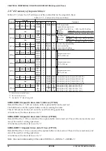
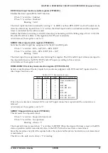
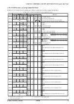
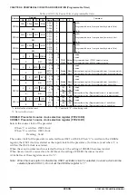
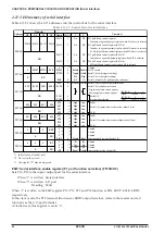
PLPOL: Timer 0 pulse polarity selection register (FFC0H•D0)
Selects the count pulse polarity in the event counter mode.
When "1" is written: Rising edge
When "0" is written: Falling edge
Reading: Valid
The count timing in the event counter mode (timer 0) is selected from either the falling edge of the
external clock input to the K13 input port terminal or the rising edge. When "0" is written to the PLPOL
register, the falling edge is selected and when "1" is written, the rising edge is selected.
Setting of this register is effective only when timer 0 is used in the event counter mode.
At initial reset, this register is set to "0".
PTSEL0: Timer 0 PWM mode selection register (FFD8H•D0)
PTSEL1: Timer 1 PWM mode selection register (FFD8H•D1)
Sets timer 0 or 1 for PWM output.
When "1" is written: PWM output
When "0" is written: Normal output
Reading: Valid
When "1" is written to the PTSELx, the compare data register becomes valid and PWM waveform is
generated using the underflow and compare match signals. When "0" is written, the timer outputs the
normal clock generated from the underflow signal. When timers 0 and 1 are used as a 16-bit timer, the
setting of PTSEL1 becomes invalid.
At initial reset, these registers are set to "0".
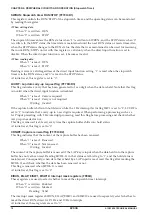
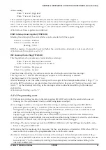
RLD00–RLD07: Timer 0 reload data register (FFC6H, FFC7H)
RLD10–RLD17: Timer 1 reload data register (FFC8H, FFC9H)
Sets the initial value for the counter.
The reload data written in this register is loaded to the respective counters. The counter counts down
using the data as the initial value for counting.
Reload data is loaded to the counter when the counter is reset by writing "1" to the PTRSTx register, or
when counter underflow occurs.
At initial reset, these registers are set to "00H".
PTD00–PTD07: Timer 0 counter data (FFCCH, FFCDH)
PTD10–PTD17: Timer 1 counter data (FFCEH, FFCFH)
Count data in the programmable timer can be read from these latches.
The low-order 4 bits of the count data in timer x can be read from PTDx0–PTDx3, and the high-order data
can be read from PTDx4–PTDx7. Since the high-order 4 bits are held by reading the low-order 4 bits, be
sure to read the low-order 4 bits first.
Since these latches are exclusively for reading, the writing operation is invalid.
At initial reset, these counter data are set to "00H".
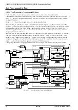
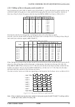
CD00–CD07: Timer 0 compare data register (FFD2H, FFD3H)
CD10–CD17: Timer 1 compare data register (FFD4H, FFD5H)
Set the compare data for PWM output.
When the timer is set in the PWM mode, the compare data set in this register is compared with the
counter data and outputs the compare match signal if they are matched. The compare match signal is
used for generating an interrupt and controlling the duty ratio of the PWM waveform.
At initial reset, these registers are set to "00H".
Содержание S1C63656
Страница 1: ...Technical Manual CMOS 4 BIT SINGLE CHIP MICROCOMPUTER S1C63656 Technical Hardware S1C63656 ...
Страница 4: ......
Страница 6: ......

