90
EPSON
S1C63656 TECHNICAL MANUAL
CHAPTER 4: PERIPHERAL CIRCUITS AND OPERATION (Serial Interface)
Serial data input procedure and interrupt
The S1C63656 serial interface is capable of inputting serial data as parallel data, in units of 8 bits.
The serial data is input from the SIN (P10) terminal, synchronizes with the synchronous clock, and is
sequentially read in the 8-bit shift register. The synchronous clock used here is as follows: in the
master mode, internal clock which is output to the SCLK (P12) terminal while in the slave mode,
external clock which is input from the SCLK (P12) terminal.
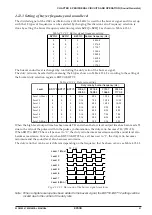
Shift timing of serial data is as follows:
• When positive polarity is selected for the synchronous clock (mask option):
The serial data is read into the built-in shift register at the rising edge of the SCLK signal when the
SCPS register is "1" and is read at the falling edge of the SCLK signal when the SCPS register is "0".
The shift register is sequentially shifted as the data is fetched.
• When negative polarity is selected for the synchronous clock (mask option):
_________
The serial data is read into the built-in shift register at the falling edge of the SCLK signal when the
_________
SCPS register is "1" and is read at the rising edge of the SCLK signal when the SCPS register is "0". The
shift register is sequentially shifted as the data is fetched.
When the input of the 8-bit data from SD0 to SD7 is completed, the interrupt factor flag ISIF is set to
"1" and an interrupt is generated. Moreover, the interrupt can be masked by the interrupt mask
register EISIF. However, regardless of the interrupt mask register setting, the interrupt factor flag is
set to "1" after input of the 8-bit data.
The data input in the shift register can be read from data registers SD0–SD7 by software.
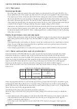
Serial data input/output permutation
The S1C63656 allows the input/output permutation of serial data to be selected by the SDP register
(FF71H•D3) as to either LSB first or MSB first. The block diagram showing input/output permutation
in case of LSB first and MSB first is provided in Figure 4.11.4.1. The SDP register should be set before
setting data to SD0–SD7.
SIN
SIN
Address [FF73H]
Address [FF72H]
Address [FF73H]
Address [FF72H]
Output
latch
Output
latch
SOUT
SOUT
SD3 SD2 SD1 SD0
SD4 SD5 SD6 SD7
SD7 SD6 SD5 SD4
SD0 SD1 SD2 SD3
(LSB first)
(MSB first)
Fig. 4.11.4.1 Serial data input/output permutation
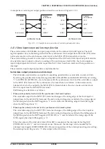
SRDY signal
When the S1C63656 serial interface is used in the slave mode (external clock mode), SRDY signal is
used to indicate whether the internal serial interface is available to transmit or receive data for the
master side (external) serial device. SRDY signal is output from the SRDY (P13) terminal.
Output timing of SRDY signal is as follows:
• When positive polarity is selected (mask option):
SRDY signal goes "1" (high) when the S1C63656 serial interface is available to transmit or receive data;
normally, it is at "0" (low).
SRDY signal changes from "0" to "1" immediately after "1" is written to SCTRG and returns from "1" to
"0" when "1" is input to the SCLK (P12) terminal (i.e., when the serial input/output begins transmit-
ting or receiving data). Moreover, when high-order data is read from or written to SD4–SD7, the SRDY
signal returns to "0".
• When negative polarity is selected (mask option):
_________
SRDY signal goes "0" (low) when the S1C63656 serial interface is available to transmit or receive data;
normally, it is at "1" (high).
_________
SRDY signal changes from "1" to "0" immediately after "1" is written to SCTRG and returns from "0" to
_________
"1" when "0" is input to the SCLK (P12) terminal (i.e., when the serial input/output begins transmit-
_________
ting or receiving data). Moreover, when high-order data is read from or written to SD4–SD7, the SRDY
signal returns to "1".
Содержание S1C63656
Страница 1: ...Technical Manual CMOS 4 BIT SINGLE CHIP MICROCOMPUTER S1C63656 Technical Hardware S1C63656 ...
Страница 4: ......
Страница 6: ......

