140
EPSON
S1C63656 TECHNICAL MANUAL
CHAPTER 5: SUMMARY OF NOTES
Output port
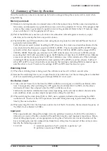
(1) When using the output port (R02, R03) as the special output port, fix the data register (R02, R03) at "1"
and the high impedance control register (R02HIZ, R03HIZ) at "0" (data output).
Be aware that the output terminal is fixed at a low (V
SS
) level the same as the DC output if "0" is
written to the R02 and R03 registers when the special output has been selected.
Be aware that the output terminal shifts into high impedance status when "1" is written to the high
impedance control register (R02HIZ, R03HIZ).
(2) A hazard may occur when the FOUT signal and the TOUT signal are turned on and off.
(3) When f
OSC3
is selected for the FOUT signal frequency, it is necessary to control the OSC3 oscillation
circuit before output. Refer to Section 4.3, "Oscillation Circuit", for the control and notes.
f
OSC3
is available when a mask option for using the OSC3 oscillation circuit is selected. If the system
uses the OSC1 oscillation circuit only, do not set the FOFQ register to "11".
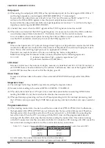
I/O port
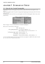
When in the input mode, I/O ports are changed from high to low by pull-down resistor, the fall of the
waveform is delayed on account of the time constant of the pull-down resistor and input gate capaci-
tance. Hence, when fetching input ports, set an appropriate wait time.
Particular care needs to be taken of the key scan during key matrix configuration.
Make this waiting time the amount of time or more calculated by the following expression.
10
×
C
×
R
C: terminal capacitance 5 pF + parasitic capacitance ? pF
R: pull-down resistance 375 k
Ω
(Max.)
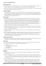
LCD driver
Because at initial reset, the contents of display memory are undefined and LC3–LC0 (LCD contrast) is
set to 0000B, there is need to initialize by the software. Furthermore, take care of the registers LPWR
and ALOFF because these are set so that the display goes off.
Clock timer
Be sure to read timer data in the order of low-order data (TM0–TM3) then high-order data (TM4–
TM7).
Stopwatch timer
(1) The interrupt factor flag should be reset after resetting the stopwatch timer.
(2) Be sure to data reading in the order of SWD0–3
→
SWD4–7
→
SWD8–11.
(3) When data that is held by a LAP input is read, read the capture buffer renewal flag CRNWF after
reading the SWD8–11 and check whether the data has been renewed or not.
(4) When performing a processing such as a LAP input preceding with 1 Hz interrupt processing, read
the LAP data carry-up request flag LCURF before processing and check whether carry-up is needed or
not.
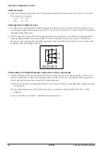
Programmable timer
(1) When reading counter data, be sure to read the low-order 4 bits (PTDx0–PTDx3) first. Furthermore,
the high-order 4 bits (PTDx4–PTDx7) are not latched when the low-order 4 bits are read. Therefore,
the high-order 4 bits should be read within 0.73 msec (when f
OSC1
is 32.768 kHz) from reading the
low-order 4 bits. When the CPU is running with the OSC1 clock and the programmable timer is
running with the OSC3 clock, stop the timer before reading the counter data. The counter running
with OSC3 counts down for the value listed in Table 5.2.1 while the CPU running with OSC1 reads the
low-order 4 bits and high-order 4 bits of the counter data by two instructions.
Table 5.2.1 Counter change with OSC3 between readings low-order and high-order data with OSC1
Count clock
OSC3/1
OSC3/4
OSC3/32
Counter change between reading
0200H
001AH
0002H
In 16-bit mode, the counter data must be read in the order below.
PTD00–PTD03
→
PTD04–PDT07
→
PTD10–PTD13
→
PTD14–PTD17
Содержание S1C63656
Страница 1: ...Technical Manual CMOS 4 BIT SINGLE CHIP MICROCOMPUTER S1C63656 Technical Hardware S1C63656 ...
Страница 4: ......
Страница 6: ......


