80
EPSON
S1C63656 TECHNICAL MANUAL
CHAPTER 4: PERIPHERAL CIRCUITS AND OPERATION (Programmable Timer)
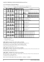
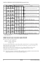
Table 4.10.10.1(b) Control bits of programmable timer
Address
Comment
D3
D2
Register
D1
D0
Name
Init
∗
1
1
0
FFE0H
0
0
ECTC1 ECTC0
R
R/W
0
∗
3
0
∗
3
ECTC1
ECTC0
–
∗
2
–
∗
2
0
0
Enable
Enable
Mask
Mask
Unused
Unused
Interrupt mask register (Programmable timer 1 compare match)
Interrupt mask register (Programmable timer 0 compare match)
CD07
CD06
CD05
CD04
0
0
0
0
MSB
Programmable timer 0 compare data (high-order 4 bits)
LSB
R/W
FFD3H
CD07
CD06
CD05
CD04
CD17
CD16
CD15
CD14
0
0
0
0
MSB
Programmable timer 1 compare data (high-order 4 bits)
LSB
R/W
FFD5H
CD17
CD16
CD15
CD14
CD13
CD12
CD11
CD10
0
0
0
0
MSB
Programmable timer 1 compare data (low-order 4 bits)
LSB
R/W
FFD4H
CD13
CD12
CD11
CD10
FFF0H
0
0
ICTC1
ICTC0
R
R/W
0
∗
3
0
∗
3
ICTC1
ICTC0
–
∗
2
–
∗
2
0
0
(R)
Yes
(W)
Reset
(R)
No
(W)
Invalid
Unused
Unused
Interrupt factor flag (Programmable timer 1 compare match)
Interrupt factor flag (Programmable timer 0 compare match)
FFD8H
0
0
PTSEL1 PTSEL0
R
R/W
0
∗
3
0
∗
3
PTSEL1
PTSEL0
–
∗
2
–
∗
2
0
0
PWM
PWM
Normal
Normal
Unused
Unused
Programmable timer 1 PWM output selection
Programmable timer 0 PWM output selection
FFF1H
0
0
IPT1
IPT0
R
R/W
0
∗
3
0
∗
3
IPT1
IPT0
–
∗
2
–
∗
2
0
0
(R)
Yes
(W)
Reset
(R)
No
(W)
Invalid
Unused
Unused
Interrupt factor flag (Programmable timer 1 underflow)
Interrupt factor flag (Programmable timer 0 underflow)
FFE1H
0
0
EIPT1
EIPT0
R
R/W
0
∗
3
0
∗
3
EIPT1
EIPT0
–
∗
2
–
∗
2
0
0
Enable
Enable
Mask
Mask
Unused
Unused
Interrupt mask register (Programmable timer 1 underflow)
Interrupt mask register (Programmable timer 0 underflow)
*1 Initial value at initial reset
*3 Constantly "0" when being read
*2 Not set in the circuit
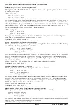
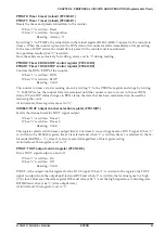
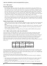
CKSEL0: Prescaler 0 source clock selection register (FFC2H•D0)
CKSEL1: Prescaler 1 source clock selection register (FFC2H•D1)
Selects the source clock of the prescaler.
When "1" is written: OSC3 clock
When "0" is written: OSC1 clock
Reading: Valid
The source clock for the prescaler is selected from OSC1 or OSC3. When "0" is written to the CKSELx
register, the OSC1 clock is selected as the input clock for the prescaler x (for timer x) and when "1" is
written, the OSC3 clock is selected.
When the event counter mode is selected for timer 0, the setting of CKSEL0 becomes invalid.
When timers 0 and 1 are used as a 16-bit timer, the setting of CKSEL1 becomes invalid.
At initial reset, these registers are set to "0".
Note: When the mask option to disable the OSC3 oscillation circuit is selected, no source clock can be
selected (fixed at OSC1). Do not set the CKSELx register to "1".
Содержание S1C63656
Страница 1: ...Technical Manual CMOS 4 BIT SINGLE CHIP MICROCOMPUTER S1C63656 Technical Hardware S1C63656 ...
Страница 4: ......
Страница 6: ......

