S1C63656 TECHNICAL MANUAL
EPSON
41
CHAPTER 4: PERIPHERAL CIRCUITS AND OPERATION (Output Ports)
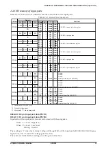
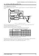
4.5.5 I/O memory of output ports
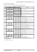
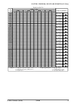
Table 4.5.5.1 shows the I/O addresses and control bits for the output ports.
Table 4.5.5.1 Control bits of output ports
Address
Comment
D3
D2
Register
D1
D0
Name
Init
∗
1
1
0
FF06H
FOUTE SWDIR FOFQ1 FOFQ0
R/W
FOUTE
SWDIR
FOFQ1
FOFQ0
0
0
0
0
Enable
Disable
FOUT output enable
Stopwatch direct input switch
0: K00=Run/Stop, K01=Lap 1: K00=Lap, K01=Run/Stop
FOUT
frequency
selection
0
f
OSC1
/64
1
f
OSC1
/8
2
f
OSC1
3
f
OSC3
[FOFQ1, 0]
Frequency
FF30H
R03HIZ R02HIZ R01HIZ R00HIZ
R/W
R03HIZ
R02HIZ
R01HIZ
R00HIZ
0
0
0
0
Hi-Z
Hi-Z
Hi-Z
Hi-Z
Output
Output
Output
Output
R03 (FOUTE=0)/FOUT (FOUTE=1) Hi-Z control
R02 (PTOUT=0)/TOUT (PTOUT=1) Hi-Z control
R01 Hi-Z control
R00 Hi-Z control
FF31H
R03
R02
R01
R00
R/W
R03
R02
R01
R00
0
0
0
0
High
High
High
High
Low
Low
Low
Low
R03 output port data (FOUTE=0) Fix at "1" when FOUT is used.
R02 output port data (PTOUT=0) Fix at "1" when TOUT is used.
R01 output port data
R00 output port data
0
∗
3
0
∗
3
CHSEL0
PTOUT
–
∗
2
–
∗
2
0
0
Timer 1
On
Timer 0
Off
Unused
Unused
TOUT output selection
TOUT output control
R
R/W
FFC1H
0
0
CHSEL0 PTOUT
*1 Initial value at initial reset
*2 Not set in the circuit
*3 Constantly "0" when being read
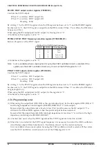
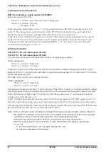
R00HIZ–R03HIZ: R0 port high impedance control register (FF30H)
Controls high impedance output of the output port.
When "1" is written: High impedance
When "0" is written: Data output
Reading: Valid
By writing "0" to the high impedance control register, the corresponding output terminal outputs accord-
ing to the data register. When "1" is written, it shifts into high impedance status.
When the output ports R02 and R03 are used for special output (TOUT, FOUT), fix the R02HIZ register
and the R03HIZ register at "0" (data output).
At initial reset, these registers are set to "0".
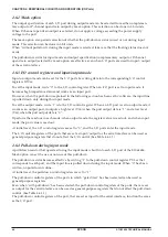
R00–R03: R0 output port data register (FF31H)
Set the output data for the output ports.
When "1" is written: High level output
When "0" is written: Low level output
Reading: Valid
The output port terminals output the data written in the corresponding data registers without changing
it. When "1" is written to the register, the output port terminal goes high (V
DD
), and when "0" is written,
the output port terminal goes low (V
SS
).
When the output ports R02 and R03 are used for special output (TOUT, FOUT), fix the R02 register and
the R03 register at "1".
At initial reset, these registers are all set to "0".
Содержание S1C63656
Страница 1: ...Technical Manual CMOS 4 BIT SINGLE CHIP MICROCOMPUTER S1C63656 Technical Hardware S1C63656 ...
Страница 4: ......
Страница 6: ......


