18 UNIVERSAL SERIAL INTERFACE (USI)
S1C33L26 TECHNICAL MANUAL
Seiko Epson Corporation
18-9
Data reception
In SPI master mode, write dummy data to the transmit data buffer. Writing to the transmit data buffer creates
the trigger for reception as well as transmission start. Writing actual transmit data enables simultaneous trans-
mission and reception. This starts the SPI clock output from the USI_CK pin.
In SPI slave mode, the module waits until the clock is input from the USI_CK pin. There is no need to write to
the transmit data buffer if no transmission is required. The receiving operation is started by the clock input from
the master device. If data is transmitted simultaneously, write transmit data to the transmit data buffer before
the clock is input.
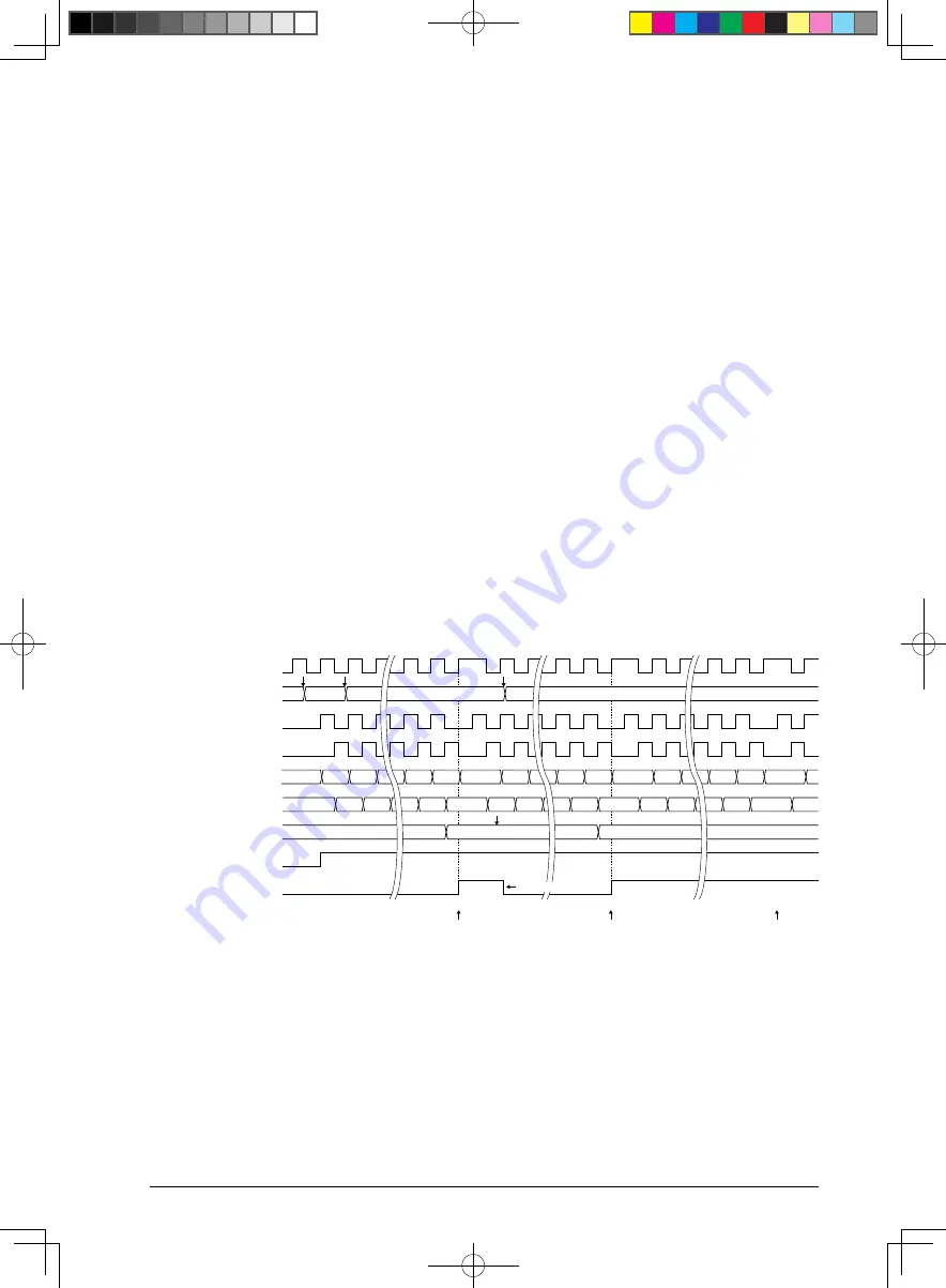
The data is received in sequence in the shift register at the SPI clock edge (see Figure 18.4.5.1). The received
data is loaded into the receive data buffer once the 8 bits of data are received in the shift register.
The received data in the buffer can be read from RD[7:0]/USI_RD register.
The SPI controller includes two status flags for transfer control: SRDIF/USI_SIF register and SSIF/USI_SIF
register.
The SRDIF flag indicates the receive data buffer status. This flag is set to 1 when the data received in the shift
register is loaded into the receive data buffer, indicating that the received data can be read out. SRDIF is an
interrupt flag. An interrupt or DMA request can be generated when this flag is set to 1 (see Section 18.7). Read
the received data from the receive data buffer using this interrupt or DMA. The receive data buffer size is 1
byte, therefore the received data must be read before the subsequent data reception has completed. Furthermore,
SRDIF must be reset by writing 1. While SRDIF is set to 1, the next received data will not be transferred from
the shift register to the receive data buffer (the first byte data exists in the receive data buffer and the second
byte data exists in the shift register). An overrun error occurs if the third byte data is received in this condition,
as the second byte data in the shift register is corrupted (an overrun error occurs at the time the first bit of the
third byte is fetched).
In SPI master mode, the SSIF flag indicates the shift register status. This flag switches to 1 at the beginning of
data reception and reverts to 0 once the data is received. Read this flag to check whether the SPI controller is
operating or at standby.
spi_ck (master mode)
TD[7:0]
USI_CK pin
(SCPOL = 0, SCPHA = 1)
USI_CK pin
(SCPOL = 0, SCPHA = 0)
USI_DI pin
Shift register
RD[7:0]
SSIF (master mode)
SRDIF
Interrupt
A
D7
A
D6
A
D1
A
D0
B
D1
B
D0
Write
Write
Write
Receive buffer full interrupt
Receive buffer full interrupt
Overrun error interrupt
(when Data B has not been read)
(MSB first)
dummy
dummy
Data A
Data B
dummy
B
D7
B
D6
C
D1
C
D0
C
D7
C
D6
Read
D
D7
Reset by writing 1
5.2.2 Data Receiving Timing Chart (SPI mode)
Figure 18.
Slave select signal
In SPI slave mode, data transmission/receiving operations are enabled when the master device's slave select
signal input to the USI_CS pin is low. When the slave select signal is high, the SPI controller does not start data
transfer even if the clock is input to the USI_CK pin from the master device. The slave select signal status can
be checked using SSIF/USI_SIF register (it functions as the shift register status flag in SPI master mode). SSIF
goes 1 when the slave select signal is inactive (high); it goes 0 when the slave select signal is active (low).
If a slave select output is required in SPI master mode, use a general-purpose I/O port and control its output
with software.


