20 GENERAL-PURPOSE SERIAL INTERFACE (FSIO)
20-16
Seiko Epson Corporation
S1C33L26 TECHNICAL MANUAL
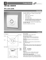
Example: Data length: 8 bits, Stop bit: 1 bit, Parity bit: Included
S1
S2
P
Start bit
Stop bit
Parity bit
A
B
First data is written. (2 bytes)
Next data is written. (2 bytes)
Transmit-buffer empty
interrupt request
Transmit-buffer empty
interrupt request
Sampling clock
SOUT
x
TDBE
TEND
S1 D0 D1 D2 D3 D4 D5 D6 D7 P S2 S1 D0 D1
D7 P S2 S1 D0 D1
D7 P S2 S1 D0 D1
D7 P S2
A
B
*
*
: 1 PCLK cycle
*
7.3.1 Transmit Timing Chart in Asynchronous Mode
Figure 20.
1. The contents of the buffer are transferred to the shift register synchronously with the first falling edge of the
sampling clock. At the same time, the SOUT
x
pin is setting to a low level to send the start bit.
2. Each bit of data in the shift register is transmitted beginning with the LSB at each falling edge of the subse-
quent sampling clock. This operation is repeated until all 8 (or 7) bits of data are transmitted.
3. After sending the MSB, the parity bit (if EPR = 1) and the stop bit are transmitted in succession.
4. The next data transfer begins if the transmit data buffer contains other data.
(3) Terminating transmit operations
When data transmission is completed, write 0 to the transmit-enable bit TXEN to disable transmit operations.
This operation clears (initializes) the transmit data buffer (FIFO), therefore, make sure that the transmit data
buffer does not contain any data waiting for transmission before writing 0 to TXEN.
Receive control
(1) Enabling receive operations
Use the receive-enable bit RXEN/FSIO_CTL
x
register for receive control.
When receiving enabled by writing 1 to this bit, clock input to the shift register is enabled (ready for input),
meaning that it is ready to receive data. Receive operations are disabled and the receive data buffer (FIFO) is
cleared (initialized) by writing 0 to RXEN.
Note: Do not set RXEN to 0 during a receive operation.
(2) Receive procedure
This serial interface has a receive shift register, receive data buffer and a receive data register that are provided
independently of those used for transmit operations.
The received data enters the received data buffer. The receive data buffer is a 4-byte FIFO and can receive data
until it becomes full unless the received data is not read out.
The received data in the buffer can be read by accessing RXD[7:0]/FSIO_RXD
x
register. The older data is out-
put first and cleared by reading.
The number of data in the receive data buffer can be checked by reading RXDNUM[1:0]/FSIO_STATUS
x
reg-
ister. When RXDNUM[1:0] is 0, the buffer contains 0 or 1 data. When RXDNUM[1:0] is 1–3, the buffer con-
tains 2–4 data.
Furthermore, RDBF/FSIO_STATUS
x
register is provided for indicating whether the receive data buffer is emp-
ty or not. This flag is set to 1 when the receive data buffer contains one or more received data, and is reset to 0
when the receive data buffer becomes empty by reading all the received data.
When the receive data buffer has received the specified number or more data (one in standard mode or one to
four in advanced mode), a cause of the receive-buffer full interrupt occurs. Since an interrupt can be generated
by setting the interrupt control bits, the received data can be read by an interrupt processing routine.