


Product Description
Rev. A
1-33
1.4.2 Serial Interface
Synchronization
Asynchronous
Signal level
EIA-232D
MARK (logical 1):
-3 V to -25 V
SPACE (logical):
+3 V to +25 V
Word format
Start bit:
1 bit
Data bit:
8 bit
Parity bit:
Odd, Even or Non
Stop bit:
1 bit
Baud rate
300, 600, 1200, 2400, 4800, 9600 or 19200 bps
Handshaking
DTR signal and XON/XOFF
DTR = MARK, XOFF:
Indicates that the printer cannot receive data.
DTR = SPACE, XON:
Indicates that the printer is ready to receive data.
The DTR signal is MARK and XOFF code (DC3, 13H) is transmitted when the rest of
the input buffer becomes 256 byte. The DTR signal is SPACE and XON code (DC1,
11H) is transmitted when the rest of the input buffer becomes 256 byte.
Error handling
Parity error is detected only.
(Overrun error and framing error are ignored.)
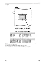
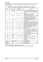
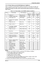
Connector
25-pin sub-miniature D-shell connector. (female)
Table 1-27. Connector Pin Assignment for Serial Interface
Pin No.
Signal Name
I/O
Function Description
1
Chassis GND
Chassis GND
2
TXD
Out
Transmits data
3
RXD
In
Receives data
4
RTS
Out
Request to send. Always SPACE level
when the printer is powered on. Pulled
up to +12 V via 4.7 L ohm resistor.
7
Signal GND
Signal GND
11
REV
Out
Connected directly to the DTR signal.
20
DTR
Out
Data terminal ready
others
NC
Not used. Not connected.
Note: In and Out refers to the direction of the signal flow from the printer’s point of
view.
Содержание DLQ-3000 Minerva+
Страница 1: ...EPSON 24 PIN DOT MATRIX PRINTER EPSON DLQ 3000 SERVICE MANUAL SEIKO EPSON CORPORATION 4008259 ...
Страница 5: ...v REVISION SHEET Revision Issued Data Contents Rev A August 21 1997 First Release ...
Страница 61: ...2 3 12 Other Sensor Circuits 2 31 ...
Страница 160: ...Chapter 6 Maintenance 6 1 Maintenance 6 1 6 1 1 Lubrication and Adhesion 6 1 ...
Страница 171: ...DLQ 3000 Rev A A 6 ...
Страница 172: ...Appendix Rev A A 7 A 2 Circuit Diagrams Figure A 2 C210 MAIN Board Circuit Diagram 1 2 ...
Страница 173: ...DLQ 3000 Rev A A 8 ...
Страница 174: ...Appendix Rev A A 9 Figure A 3 C210 MAIN Board Circuit Diagram 2 2 ...
Страница 175: ...DLQ 3000 Rev A A 10 ...
Страница 177: ...DLQ 3000 Rev A A 12 Figure A 5 C124 PSB Board Circuit Diagram ...
Страница 179: ...DLQ 3000 Rev A A 14 A 3 Circuit Board Component Layout Figure A 7 C210 MAIN Board Component Layout 1 2 ...
Страница 180: ...Appendix Rev A A 15 Figure A 8 C210 MAIN Board Component Layout 2 2 ...
Страница 181: ...DLQ 3000 Rev A A 16 Figure A 9 C124 PSB Board Component Layout ...
Страница 182: ...Appendix Rev A A 17 Figure A 10 C124 PSE Board Component Layout ...
Страница 189: ...EPSON SEIKO EPSON CORPORATION ...