

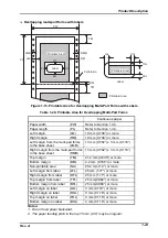


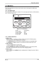
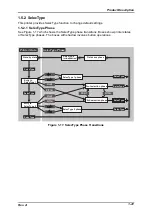


Product Description
Rev. A
1-31
Reverse Channel
Transmission mode
IEEE-1284 nibble mode
Adaptable connector
Same as for the forward channel
Synchronization
Refer to the IEEE-1284 specification
Handshaking
Refer to the IEEE-1284 specification
Data transmission timing
Refer to the IEEE-1284 specification
Signal level
IEEE-1284 level 1 device
See the forward channel.
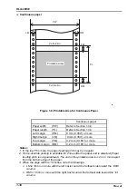
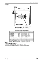
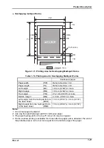
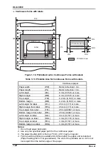
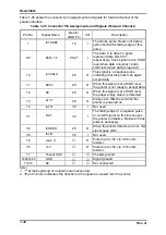
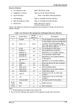
Table 1-26 shows the connector pin assignment and signals for reverse channel of the
parallel interface.
Table 1-26. Connector Pin Assignment and Signals (Reverse Channel)
Pin No.
Signal Name
Return
GND Pin
I/O
Description
1
HostClk
19
I
Clock signal from the host computer.
2-9
DATA 1-8
20-27
I
These signals represent parallel data
on bits 2 to 9. Each signal is High
when the data is logical 1 and LOW
when the data is logical 0.
10
PtrClk
28
O
Clock signal from the printer
11
PtrBusy /
Data bit 3,7
29
O
Busy signal from the printer.
Data bit 3 or 7 in reverse channel.
12
AckDatareq /
Data Bit 2,6
28
O
Acknowledge request signal.
Data bit 2 or 6 in reverse channel.
13
Xflag/Data bit
1,5
28
O
X flag signal.
Data bit 1 or 5 in reverse channel.
14
HostBusy
30
I
Busy signal from the host computer
31
/INIT
30
I
Not used
32
/Data Avail /
Data bit 0,4
29
O
Data available signal.
Data bit 0 or 4 in reverse channel.
36
1284-Active
30
I
1284 active signal.
18
Logic-H
O
Pulled up to +5V via 3.9 K-ohm
resistor.
35
+5V
O
Pulled up to +5V via 3.3 K-ohm
resistor.
17
Chassis GND
Chassis ground for the printer.
16,33,
19-30
GND
Signal ground.
15,34
NC
Not connected.
Note)
1. */* at the beginning of a signal means active low.
2. The I/O column indicates the direction of the signal as viewed form the printer.
Содержание DLQ-3000 Minerva+
Страница 1: ...EPSON 24 PIN DOT MATRIX PRINTER EPSON DLQ 3000 SERVICE MANUAL SEIKO EPSON CORPORATION 4008259 ...
Страница 5: ...v REVISION SHEET Revision Issued Data Contents Rev A August 21 1997 First Release ...
Страница 61: ...2 3 12 Other Sensor Circuits 2 31 ...
Страница 160: ...Chapter 6 Maintenance 6 1 Maintenance 6 1 6 1 1 Lubrication and Adhesion 6 1 ...
Страница 171: ...DLQ 3000 Rev A A 6 ...
Страница 172: ...Appendix Rev A A 7 A 2 Circuit Diagrams Figure A 2 C210 MAIN Board Circuit Diagram 1 2 ...
Страница 173: ...DLQ 3000 Rev A A 8 ...
Страница 174: ...Appendix Rev A A 9 Figure A 3 C210 MAIN Board Circuit Diagram 2 2 ...
Страница 175: ...DLQ 3000 Rev A A 10 ...
Страница 177: ...DLQ 3000 Rev A A 12 Figure A 5 C124 PSB Board Circuit Diagram ...
Страница 179: ...DLQ 3000 Rev A A 14 A 3 Circuit Board Component Layout Figure A 7 C210 MAIN Board Component Layout 1 2 ...
Страница 180: ...Appendix Rev A A 15 Figure A 8 C210 MAIN Board Component Layout 2 2 ...
Страница 181: ...DLQ 3000 Rev A A 16 Figure A 9 C124 PSB Board Component Layout ...
Страница 182: ...Appendix Rev A A 17 Figure A 10 C124 PSE Board Component Layout ...
Страница 189: ...EPSON SEIKO EPSON CORPORATION ...