background image

DL205 Analog Manual, 7th Edition Rev. D

14-18

Chapter 14: F2-4AD2DA, 4-Ch. In / 2-Ch. Out Analog Combination

1
2
3
4
5
6
7
8
9

10
11
12
13
14

A

B

C

D

1
2
3
4
5
6
7
8
9

10
11
12
13
14

A

b

C

D

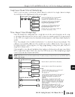
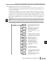
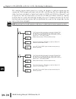
Read Input Values (Multiplexing)

The DL230 CPU does not use special V-memory locations for transferring data. Since all 

channels are multiplexed into a single data word, the control program must be setup to 

determine which channel is being read. Since the module appears as X input points to the 

CPU, simply use the active channel status bits to determine which channel is being read.
Note, this example is for a module installed in slot 3, as shown in the previous examples. The 

addresses used would be different if the module was used in a different slot. These rungs can 

be placed anywhere in the program or if stage programming is being used, place them in a 

stage that is always active.
This multiplexing example can be used with all of the DL205 CPUs.

It is usually easier to perform math operations in

BCD, You can leave out this instruction if your

application does not require it.

This instruction masks the channel identification bits.

Without this, the values used will not be correct so do

not forget to include it.

Loads the complete data word into the accumulator.

The V-memory location depends on the I/O

configuration. See Appendix A for the memory map.

Load data when module is not busy.

LD

V40401

ANDD

KFFF

BCD

X36

X36

X34

X35

Store Channel 1

OUT

V2000

When the module is not busy and X36, X34 and X35

are off, channel 1 data is stored in V2000.

When the module is not busy and X34 is on and X35

and X36 are off, channel 2 data is stored in V2001.

When the module is not busy and X34 and X36 are

off and X35 is on, channel 3 data is stored in V2002.

When the module is not busy and both X34 and X35 are

on and X36 is off, channel 4 data is stored in V2003.

X36

X34

X35

Store Channel 2

OUT

V2001

X36

X34

X35

Store Channel 3

OUT

V2002

X36

X34

X35

Store Channel 4

OUT

V2003

Содержание DL205

Страница 1: ...DL205 Analog I O Manual Manual Number D2 ANLG M ...

Страница 2: ...Notes ...

Страница 3: ...t in hazardous environments requiring fail safe performance such as in the operation of nuclear facilities aircraft navigation or communication systems air traffic control direct life support machines or weapons systems in which the failure of the product could lead directly to death personal injury or severe physical or environmental damage High Risk Activities AutomationDirect specifically discl...

Страница 4: ...reux nécessitant une sécurité absolue par exemple l exploitation d installations nucléaires les systèmes de navigation aérienne ou de communication le contrôle de la circulation aérienne les équipements de survie ou les systèmes d armes pour lesquels la défaillance du produit peut provoquer la mort des blessures corporelles ou de graves dommages matériels ou environnementaux activités à risque éle...

Страница 5: ... Added DL250 1 and DL260 CPUs and removed references to DL250 CPU Note DL250 has same functionality as a DL250 1 except for local expansion capability Rev B 8 02 Minor corrections 7th Edition 8 05 Added new F2 8AD4DA chapters 15 and 16 and miscellaneous minor changes Rev A 11 06 Added information about changes to F2 04THM jumper link locations in chapter 7 Rev B 4 10 Added information about jumper...

Страница 6: ...Notes ...
Страница 7: ...inology 1 5 Selecting the Appropriate Module 1 6 Wide Variety of Modules 1 6 Diagnostic Features 1 6 Analog Input 1 7 Special Input 1 7 Analog Output 1 8 Combination Analog 1 8 Analog Made Easy Four Steps 1 9 Chapter 2 F2 04AD 1 4 Channel Analog Current Input Module Specifications 2 2 F2 04AD 1 2 2 F2 04AD 1L is Obsolete 2 2 Input Specifications 2 3 General Specifications 2 3 Analog Input Configur...

Страница 8: ...2 13 Module Resolution 2 13 Writing the Control Program 2 14 Reading Values Pointer Method and Multiplexing 2 14 Pointer Method for the DL240 DL250 1 and DL260 2 14 Reading Values Multiplexing for the DL230 DL240 DL250 1 and DL260 2 16 Single Channel Selected 2 16 Analog Power Failure Detection 2 17 Scaling the Input Data 2 17 The Conversion Program 2 18 Analog and Digital Value Conversions 2 18 F...

Страница 9: ...4 Writing the Control Program 3 15 Reading Values Pointer Method and Multiplexing 3 15 Pointer Method for the DL240 DL250 1 and DL260 CPUs 3 15 Using Bipolar Ranges Ptr Method for the DL240 DL250 1 and DL260 CPUs 3 17 Reading Values Multiplexing for the DL230 DL240 DL250 1 and DL260 3 18 Single Channel Selected 3 19 Using Bipolar Ranges Multiplexing 3 19 Using 2 s Complement for DL230 DL240 DL250 ...

Страница 10: ...ignments 4 11 Analog Data Bits 4 11 Active Channel Indicator Inputs 4 12 Module Diagnostic Inputs 4 12 Module Resolution 4 12 Writing the Control Program 4 13 Reading Values Pointer Method and Multiplexing 4 13 Pointer Method for the DL240 DL250 1 and DL260 CPUs 4 13 Reading Values Multiplexing for the DL230 DL240 DL250 1 and DL260 4 15 Single Channel Selected 4 15 Analog Power Failure Detection 4...

Страница 11: ...ic and Sign 5 12 Module Resolution 5 12 Writing the Control Program 5 14 Reading Values Pointer Method and Multiplexing 5 14 Pointer Method for the DL240 DL250 1 and DL260 CPUs 5 14 Using Bipolar Ranges Pointer Method for the DL240 DL250 1 and DL260 CPUs 5 16 Reading Values Multiplexing for the DL230 DL240 DL250 1 and DL260 5 17 Single Channel Selected 5 18 Using Bipolar Ranges Multiplexing 5 18 U...

Страница 12: ...11 Reading Values Pointer Method and Multiplexing 6 11 Pointer Method for the DL240 250 1 260 CPUs 6 11 Negative Temperature Readings with Magnitude Plus Sign for the DL240 DL250 1 and DL260 CPUs Pointer Method 6 13 Magnitude Plus Sign Binary 6 14 Magnitude Plus Sign BCD 6 14 Negative Temperatures 2 s Complement for the DL240 DL250 1 and DL260 CPUs Binary Pointer Method 6 15 Understanding the Inpu...

Страница 13: ...8 Thermocouples 7 9 Ambient Variations in Temperature 7 9 Wiring Diagrams 7 10 Module Operation 7 11 Channel Scanning Sequence for a DL230 CPU Multiplexing 7 11 Channel Scanning Sequence for DL240 DL250 1 and DL260 CPUs Pointer Method 7 12 Analog Module Updates 7 12 Writing the Control Program 7 13 Reading Values Pointer Method and Multiplexing 7 13 Pointer Method for the DL240 250 1 260 CPUs 7 13...

Страница 14: ... Specifications 8 3 General Specifications 8 3 Special Placement Requirements DL230 and Remote I O Bases 8 4 Connecting and Disconnecting the Field Wiring 8 5 Wiring Guidelines 8 5 User Power Supply Requirements 8 5 Wiring Diagram 8 6 Load Range 8 6 Module Operation 8 7 Channel Scanning Sequence for a DL230 CPU Multiplexing 8 7 Channel Scanning Sequence for DL240 DL250 1 and DL260 CPUs Pointer Met...

Страница 15: ...Wiring Diagram 9 9 Module Operation 9 10 Channel Scanning Sequence for a DL230 CPU Multiplexing 9 10 Channel Scanning Sequence for DL240 DL250 1 and DL260 CPUs Pointer Method 9 11 Understanding the Output Assignments 9 12 Channel Select Outputs 9 12 Analog Data Bits 9 13 Signal Sign Output 9 13 Bipolar Output Data 9 13 Module Resolution 9 14 Writing the Control Program 9 15 Calculating the Digital...

Страница 16: ...exing 10 7 Channel Scanning Sequence for DL240 DL250 1 and DL260 CPUs Pointer Method 10 8 Understanding the Output Assignments 10 8 Channel Select Outputs 10 9 Analog Data Bits 10 10 Output Enable 10 10 Module Resolution 10 10 Writing the Control Program 10 11 Calculating the Digital Value 10 11 The Conversion Program 10 11 Reading Values Pointer Method and Multiplexing 10 12 Pointer Method for th...

Страница 17: ...t Outputs 11 10 Analog Data Bits 11 11 Output Enable 11 11 Module Resolution 11 11 Writing the Control Program 11 12 Calculating the Digital Value 11 12 The Conversion Program 11 13 Writing Values Pointer Method and Multiplexing 11 14 Writing Values Pointer Method for the DL240 DL250 1 and DL260 CPUs 11 14 Writing Data Example Multiplexing 11 16 Writing Data Example Multiplexing continued 11 17 Wr...

Страница 18: ... for the DL240 DL250 1 and DL260 CPUs 12 13 Write Data Example Multiplexing 12 15 Write Data to One Channel 12 16 Write the same Data to Both Channels 12 16 Analog and Digital Value Conversions 12 17 Chapter 13 F2 02DAS 2 0 5V 0 10V 2 Channel Isolated Analog Out Module Specifications 13 2 Firmware Requirements 13 2 Output Specifications 13 3 General Specifications 13 3 Analog Output Configuration ...

Страница 19: ...ination Module Specifications 14 2 Input Specifications 14 2 Output Specifications 14 3 General Specifications 14 3 Combination Analog Configuration Requirements 14 3 Special Placement Requirements DL230 and Remote I O Bases 14 4 Connecting the Field Wiring 14 5 Wiring Guidelines 14 5 Loop Power Supply Requirements 14 5 Current Loop Transmitter Impedance 14 6 Wiring Diagram 14 7 Module Operation 1...

Страница 20: ...Data to Both Channels 14 20 Analog and Digital Value Conversions 14 20 Filtering Input Noise DL250 1 DL260 CPUs Only 14 21 Chapter 15 F2 8AD4DA 1 8 Ch In 4 Ch Out Current Analog Comb Module Specifications 15 2 F2 8AD4DA 1 Requirements 15 2 Input Specifications 15 3 Output Specifications 15 4 General Module Specifications 15 5 Module Placement and Configuration Requirements 15 5 Connecting the Fiel...

Страница 21: ... 15 21 Scaling the Input Data 15 22 Scaling Example 15 22 Input Engineering Unit Conversion Example 1 15 23 Input Engineering Unit Conversion Example 2 15 23 Input Engineering Unit Conversion Example 3 15 24 Input Engineering Unit Conversion Example 4 15 25 Using the Input Track and Hold Feature 15 25 Track and Hold Example 15 26 Module 16 Bit Output Resolution 15 27 Digital and Analog Output Data...

Страница 22: ...ection Bits 16 15 Writing the Control Program 16 16 Configuring the Module to Read Write I O Pointer Method DL250 1 and DL260 only 16 16 Module Configuration Example 1 16 17 Module Configuration Example 2 16 18 Module Configuration Example 3 16 19 Module 12 Bit Input Resolution 16 20 Module 14 Bit Input Resolution 16 20 Module 16 Bit Input Resolution 16 20 Analog and Digital Input Data Value Conve...

Страница 23: ...tents Calculating the Digital Output Value 16 27 Calculating Output Data Engineering Units Conversion 16 27 Appendix A DL205 Discrete I O Memory Map X Input Y Output Bit Map A 2 Control Relay Bit Map A 4 Remote I O Bit Map DL260 only A 8 Table of Contents ...

Страница 24: ...ter Chapter In This Chapter Introduction 1 2 Conventions Used 1 3 Physical Characteristics 1 3 Analog Input Module Terminology 1 4 Analog Output Module Terminology 1 5 Selecting the Appropriate Module 1 6 Analog Made Easy Four Steps 1 9 ...

Страница 25: ...acquire the analog data The User Manual also provides a more thorough description of how the I O points are assigned to the module This is all the material necessary to quickly understand the DL205 Analog I O modules Technical Support We strive to make our manuals the best in the industry We rely on your feedback to let us know if we are reaching our goal If you cannot find the solution to your pa...

Страница 26: ... Modules provide many features that make the modules easy to use With the exception of the thermocouple module the terminal blocks are removable which makes wiring a simple task All of the DL205 analog modules have normal screw terminal connectors Access the module terminals by removing the front cover not shown To remove the front cover press the tab on the lower front corner of the cover For eas...

Страница 27: ...itized and acknowledged in the PLC Linearity Error The relative accuracy of the digital representation over the entire input range Maximum Inaccuracy Maximum absolute error of the digital representation of the signal over the entire input range Factors which contribute to maximum inaccuracy are also specified separately These factors are full scale calibration error offset calibration error and ac...

Страница 28: ...ve accuracy of the digital representation over the entire output range Maximum Inaccuracy Maximum absolute error of the digital representation of the signal over the entire output range Factors which contribute to maximum inaccuracy are also specified separately These factors are full scale calibration error offset calibration error and accuracy vs temperature Accuracy vs Temperature The variation...

Страница 29: ... Simply install the module add a few lines to the RLL program That s all Analog input temperature input and analog output modules are available These modules are designed and manufactured by FACTS Engineering FACTS has been producing feature packed products for the DirectLOGIC families and compatible products for years These modules are readily identifiable by their F2 prefix in the part number Di...

Страница 30: ... in 4096 12 bit 1 in 4096 and 13 bit 1 in 8192 12 bit 1 in 4096 12 bit 1 in 4096 and 13 bit 1 in 8192 Input Type Single ended Single ended Single ended Single ended Maximum Inaccuracy w 0 5 at 25 C 77 F w 0 65 at 0 60 C 32 140 F w 0 1 at 25 C 77 F w 0 3 at 0 60 C 32 140 F w 0 1 at 25 C 77 F w 0 25 at 0 60 C 32 140 F w 0 1 at 25 C 77 F w 0 3 at 0 60 C 32 140 F See Chapter 2 3 4 5 Special Input Spec...

Страница 31: ...t 1 in 4096 16 bit 1 in 4096 Output Type Single ended Single ended 1 common See Chapter 10 11 Analog Output Specification F2 02DAS 1 F2 02DAS 2 Channels 2 8 Output Ranges 4 20 mA 0 5V 0 10V Resolution 16 bit 1 in 65536 16 bit 1 in 65536 Output Type Current sourcing Isolated See Chapter 12 13 Combination Analog Specification F2 4AD2DA Input Channels 4 Output Channels 2 Input Ranges 4 20 mA Output R...

Страница 32: ...oment to review the detailed specifications to be sure the module chosen will meet the application requirements Step 2 If applicable set the module switches and or jumpers to select number of channels the operating ranges Step 3 Connect the field wiring to the module connector Step 4 Review the module operating characteristics and write the control program 1 2 3 4 5 6 7 8 9 10 11 12 13 14 A B C D ...

Страница 33: ...DL205 Analog I O Manual 7th Edition Rev D 1 10 Chapter 1 Getting Started 1 2 3 4 5 6 7 8 9 10 11 12 13 14 A B C D Notes 1 2 3 4 5 6 7 8 9 10 11 12 13 14 A B C D ...

Страница 34: ...pter Module Specifications 2 2 Setting the Module Jumpers 2 6 Connecting the Field Wiring 2 7 Module Operation 2 10 Writing the Control Program 2 14 2 F2 04AD 1 4 Channel Analog Current Input Chapter Chapter Chapter ...

Страница 35: ...er provide digital signal processing to maintain precision analog measurements in noisy environments F2 04AD 1L is Obsolete NOTE In 2009 the F2 04AD 1L was discontinued A re designed F2 04AD 1 was released at the same time which can be powered by either 12 VDC or 24 VDC input power supplies This new module is a direct replacement for prior F2 04AD 1 and all F2 04AD 1L modules The new module is a s...

Страница 36: ...or End to End W 1 count 0 025 of full scale maximum Input Stability W 1 count Full Scale Calibration Error Offset error not included W 12 counts maximum 20 mA current input Offset Calibration Error W 7 counts maximum 4 mA current input Maximum Inaccuracy W 0 5 25 C 77 F W 0 65 0 60 C 32 140 F Accuracy vs Temperature W 50 ppm C maximum full scale calibration including maximum offset change Recommen...

Страница 37: ... and Remote I O Bases Even though the module can be placed in any slot it is important to examine the configuration if a DL230 CPU is used as can be seen in the section about Writing the Program located in this chapter V memory locations are used to extract the analog data If the module is placed so the input points do not start on a V memory boundary the instructions cannot access the data This a...

Страница 38: ...ws the V memory addresses that correspond to these X locations 1 2 3 4 5 6 7 8 9 10 11 12 13 14 A B C D F2 04AD 1 8pt Input 16pt Input 16pt Input Output 16pt 16pt Input X0 X7 X10 X27 X30 X47 X50 X67 Y0 Y17 V40401 B S L B S M X 2 0 X 3 7 X 2 7 X 3 0 V40400 B S L B S M X 0 X 1 7 X 7 X 1 0 Incorrect Slot 0 Slot 1 Slot 2 Slot 3 Slot 4 Data is split over two locations so instructions cannot access data...

Страница 39: ... if only channels 1 thru 3 are selected then channel 4 will not be active The following table shows how to use the jumpers to select the number of channels 1 2 3 4 5 6 7 8 9 10 11 12 13 14 A B C D 1 2 Jumper 1 1 2 No of Channels 1 2 1 No No 1 2 Yes No 1 2 3 No Yes 1 2 3 4 Yes Yes For example to select all 4 channels 1 4 leave both jumpers installed To select channel 1 remove both jumpers Jumper lo...

Страница 40: ...s 18 30 VDC at 80 mA The DL205 bases have built in 24 VDC power supplies that provide up to 300mA of current This may used with the F2 04AD 1 modules instead of a separate supply if only a couple of analog modules are being used It is desirable in some situations to power the transmitters separately in a location remote from the PLC This will work as long as the transmitter supply meets the voltag...

Страница 41: ...l If the transmitter being used requires a load resistance below 250 q it is not necessary to make any adjustments However if the transmitter requires a load resistance higher than 250 q a resistor will need to be added in series with the input Consider the following example for a transmitter being operated from a 30 VDC supply with a recommended load resistance of 750 q Since the module has a 250...

Страница 42: ...t connected to 0 VDC on the module then the output of the external transmitter must be isolated To avoid ground loop errors recommended 4 20 mA transmitter types are 2 or 3 wire Isolation between input signal and power supply 4 wire Isolation between input signal power supply and 4 20 mA output 2 3 4 5 6 7 8 9 10 11 12 13 14 A b C D Retaining clip Retaining clip Analog Switch DC to DC Converter 24...

Страница 43: ...per scan depending on the type of CPU being used The DL230 can obtain one channel of data per CPU scan Since there are four channels it can take up to four scans to get data for all channels Once all channels have been scanned the process starts over with channel 1 Unused channels are not processed so if only two channels are selected then each channel will be updated every other scan The multiple...

Страница 44: ...rts the signal to a 12 bit binary representation This enables the module to continuously provide accurate measurements without slowing down the discrete control logic in the RLL program For the vast majority of applications the values are updated much faster than the signal changes However in some applications the update time can be important The module takes approximately 4 milliseconds to sense ...

Страница 45: ... Since all input points are automatically mapped into V memory it is very easy to determine the location of the data word that will be assigned to the module Within these word locations the individual bits represent specific information about the analog signal Analog Data Bits The first twelve bits represent the analog data in binary format Bit Value Bit Value 0 1 6 64 1 2 7 128 2 4 8 256 3 8 9 51...

Страница 46: ...mples in the next section shows this input can be used The wiring guidelines shown earlier in this chapter provide steps that can help reduce noise problems Missing 24VDC The last diagnostic input X37 in this example indicates that 24VDC has not been applied to the card For example if the 24 VDC input power is missing or if the terminal block is loose the module will turn on this input point The m...

Страница 47: ...or in the initial stage if stage programming instructions are being used This is all that is required to read the data into V memory locations Once the data is in V memory math can be used on the data compare the data against preset values and so forth V2000 is used in the example but you can use any user V memory location In this example the module is installed in slot 2 Be sure to use the V memo...

Страница 48: ...ase Analog Input Module Slot Dependent V memory Locations Slot 0 1 2 3 4 5 6 7 No of Channels V7660 V7661 V7662 V7663 V7664 V7665 V7666 V7667 Storage Pointer V7670 V7671 V7672 V7673 V7674 V7675 V7676 V7677 Expansion Base D2 CM 1 Analog Input Module Slot Dependent V memory Locations Slot 0 1 2 3 4 5 6 7 No of Channels V36000 V36001 V36002 V36003 V36004 V36005 V36006 V36007 Storage Pointer V36010 V3...

Страница 49: ... this instruction if your application does not require it This instruction masks the channel identification bits Without this the values used will not be correct so do not forget to include it Loads the complete data word into the accumulator The V memory location depends on the I O configuration See Appendix A for the memory map Store Channel 1 when Module is not busy LD V40401 ANDD KFFF BCD OUT ...

Страница 50: ...ed for the engineering units For example if pressure PSI is to be measured from 0 0 99 9 then multiply the value by 10 in order to imply a decimal place when viewing the value with the programming software or with a handheld programmer Notice how the calculations differ when the multiplier is used V2000 K0 X37 OUT C1 Multiplexing method V memory location V2000 holds channel 1 data When a data valu...

Страница 51: ...rsions Sometimes it is useful to be able to quickly convert between the signal levels and the digital values This is especially helpful during machine startup or troubleshooting The following table provides formulas to make this conversion more simple As an example if the measured signal is 10 mA the formula can be used to easily determine the digital value that will be stored in the V memory loca...

Страница 52: ...analog and are masking the first twelve bits then it is already in binary and no conversion using the BIN instruction is needed LD V2000 SUBR V1400 BTOR SP1 BIN Loads the analog signal which is a BCD value and has been loaded from V memory location V2000 into the accumulator Contact SP1 is always on Converts the BCD value in the accumulator to binary Remember this instruction is not needed if the ...

Страница 53: ...Channel Analog Voltage Input In This Chapter Module Specifications 3 2 Setting the Module Jumpers 3 5 Connecting the Field Wiring 3 7 Module Operation 3 10 Understanding the Input Assignments 3 12 Writing the Control Program 3 15 ...

Страница 54: ...t power supplies This new module is a direct replacement for prior F2 04AD 2 and all F2 04AD 2L modules The new module is a single circuit board design and the jumper link locations are different See Setting the Module Jumpers on page 3 5 Also some specifications were changed on page 3 3 Otherwise the re designed module functions the same as the prior designs 1 2 3 4 5 6 7 8 9 10 11 12 13 14 A B C...

Страница 55: ...5 VDC Converter Type Successive appropximation Linearity Error End to End 1 count 0 025 of span maximum unipolar 2 counts maximum bipolar Input Stability 1 count Full Scale Calibration Error Offset error included 3 counts maximum Offset Calibration Error 1 count maximum 0V input Maximum Inaccuracy 0 1 25 C 77 F 0 3 0 60 C 32 140 F Accuracy vs Temperature 50ppm C full scale calibration change inclu...

Страница 56: ...es required for a DL230 CPU the first input address assigned to the module must be one of the following X locations The table also shows the V memory addresses that correspond to these X locations 1 2 3 4 5 6 7 8 9 10 11 12 13 14 A B C D Slot 0 Slot 1 Slot 2 Slot 3 Slot 4 8pt Input 8pt Input 16pt Input 16pt Input 16pt Output X0 X7 X10 X17 X20 X37 X40 X57 Y0 Y17 V40401 V40402 V40400 F2 04AD 2 MSB L...

Страница 57: ...only channels 1 thru 3 are selected then channel 4 will not be active The following table shows how to place the jumpers to select the number of channels 1 2 Jumper 1 1 2 No of Channels 1 2 1 No No 1 2 Yes No 1 2 3 No Yes 1 2 3 4 Yes Yes For example to select all 4 channels 1 4 leave both jumpers installed To select channel 1 remove both jumpers Jumper location on modules having Date Code 0609F4 a...

Страница 58: ...peration jumper not installed 1 2 3 4 5 6 7 8 9 10 11 12 13 14 A B C D Jumper J2 Install jumper J2 or J3 for 0 5V or W5V operation Remove J2 or J3 or store on a single pin for 0 10V or W10V operation Jumper J2 is located on the smaller circuit board which is on top of the motherboard Install J2 for 0 5V or W5V operation Remove J2 or store on a single pin for 0 10V or W10V operation Jumper J2 locat...

Страница 59: ... 26 4 VDC at 80mA The DL205 bases have built in 24VDC power supplies that provide up to 300mA of current This can be used instead of a separate supply if only a couple of analog modules are installed Check the power budget to be safe It is desirable in some situations to power the transmitters separately in a location remote from the PLC This will work as long as the transmitter supply meets the v...

Страница 60: ...rature coefficient is recommended If a 4 20 mA signals are used and converted to voltage using this method a broken transmitter condition can easily be detected For example if using the 0 5V range and the lowest signal for the 4 20 mA transmitter is 4mA the lowest digital value for the signal is not 0 but instead is 819 If the transmitter is working properly the smallest value would be 819 in the ...

Страница 61: ...ounded at the signal source 1 2 3 4 5 6 7 8 9 10 11 12 13 14 A b C D 24V CH1 CH2 CH3 CH4 0V CH1 CH2 CH3 CH4 F2 04AD 2 IN ANALOG 4CH 10 30VDC 5mA ANALOG IN 0 5 0 10VDC 5 10VDC 24V CH1 CH2 CH3 CH4 0V CH1 CH2 CH3 CH4 F2 04AD 2 IN 10 30VDC 5mA ANALOG IN 0 5 0 10VDC 5 10VDC ANALOG 4CH Typical User Wiring Internal Module Wiring See NOTE 1 18 26 4VDC 0VDC 5V 15V 0V 15V CH4 Voltage Transmitter CH1 Voltage...

Страница 62: ...er scan The DL230 can obtain one channel of data per CPU scan Since there are four channels it can take up to four scans to get data for all channels Once all channels have been scanned the process starts over with channel 1 Unused channels are not processed so if only two channels are selected then each channel will be updated every other scan The multiplexing method can also be used for the DL24...

Страница 63: ...sentation This enables the module to continuously provide accurate measurements without slowing down the discrete control logic in the RLL program For the vast majority of applications the values are updated much faster than the signal changes However in some applications the update time can be important The module takes approximately 10 milliseconds to sense 95 of the change in the analog signal ...

Страница 64: ...ally mapped into V memory it is very easy to determine the location of the data word that will be assigned to the module Within these word locations the individual bits represent specific information about the analog signal Analog Data Bits The first twelve bits represent the analog data in binary format Bit Value Bit Value 0 1 6 64 1 2 7 128 2 4 8 256 3 8 9 512 4 16 10 1024 5 32 11 2048 1 2 3 4 5...

Страница 65: ... when extreme environmental electrical noise problems are present The last input X37 in this example is used for two purposes Signal Sign When using bipolar ranges the value returned needs to be known if it is either positive or negative When this input is off the value stored represents a positive analog signal 0V or greater If the input is on then the value stored represents a negative input sig...

Страница 66: ... to the signal range Each count can also be expressed in terms of the signal level by using the equation shown Each count can also be expressed in terms of the signal level by using the equation shown The following table shows the smallest detectable signal change that will result in one LSB change in the data value for each input signal range 1 2 3 4 5 6 7 8 9 10 11 12 13 14 A B C D V 0V 0 4095 U...

Страница 67: ...tructions are being used This is all that is required to read the data into V memory locations Once the data is in V memory math can be used on the data compare the data against preset values and so forth V2000 is used in the example but you can use any user V memory location In this example the module is installed in slot 2 Be sure to use the V memory locations for the module placement The pointe...

Страница 68: ...Module Slot Dependent V memory Locations Slot 0 1 2 3 4 5 6 7 No of Channels V36000 V36001 V36002 V36003 V36004 V36005 V36006 V36007 Storage Pointer V36010 V36011 V36012 V36013 V36014 V36015 V36016 V36017 Expansion Base D2 CM 2 Analog Input Module Slot Dependent V memory Locations Slot 0 1 2 3 4 5 6 7 No of Channels V36100 V36101 V36102 V36103 V36104 V36105 V36106 V36107 Storage Pointer V36110 V36...

Страница 69: ...ant to be known these rungs should be placed before any other operations that use the data such as math instructions scaling operations and so forth Also if stage programming instructions are being used place these rungs in a stage that is always active Please note this logic is only needed for each channel that is using bipolar input signals The following example only shows two channels 1 2 3 4 5...

Страница 70: ...rogramming is being used place them in a stage that is always active 1 2 3 4 5 6 7 8 9 10 11 12 13 14 A B C D It is usually easier to perform math operations in BCD so it is best to convert the data to BCD immediately You can leave out this instruction if your application does not require it This instruction masks the channel identification bits Without this the values used will not be correct so ...

Страница 71: ...ction masks the channel identification bits Without this the values used will not be correct so do not forget to include it Loads the complete data word into the accumulator The V memory location depends on the I O configuration See Appendix A for the memory map Store channel 1 when module is not busy LD V40401 ANDD KFFF BCD OUT V2000 When the module is not busy and X34 and X35 are off channel 1 d...

Страница 72: ...pendix A for the memory map Load data when module is not busy LD V40401 ANDD KFFF X36 X36 X34 X35 Store Channel 1 OUT V2000 When the module is not busy and X34 and X35 are off channel 1 data is stored in V2000 C0 is reset to indicate that channel 1 s value is positive SET C0 X37 RST C0 If X37 is on then the data value represents a negative voltage C0 is set to indicate that channel 1 s value is ne...

Страница 73: ... if pressure PSI is to be measured from 0 0 99 9 then multiply the value by 10 in order to imply a decimal place when viewing the value with the programming software or with a handheld programmer Notice how the calculations differ when the multiplier is used 1 2 3 4 5 6 7 8 9 10 11 12 13 14 A B C D V2000 K0 X37 OUT C0 Multiplexing method V memory location V2000 holds channel 1 data When a data val...

Страница 74: ...er versions of analog input modules The bipolar ranges use 0 4095 for both positive and negative voltages The sign bit allows this which actually provides better resolution than those modules that do not offer a sign bit The following table provides formulas to make this conversion easier As an example if the range being used is 10V 10V and the measured signal is 6V use the formula to the right to...

Страница 75: ... bits then it is already in binary and no conversion using the BIN instruction is needed 1 2 3 4 5 6 7 8 9 10 11 12 13 14 A B C D LD V2000 SUBR V1400 BTOR SP1 BIN Loads the analog signal which is a BCD value and has been loaded from V memory location V2000 into the accumulator Contact SP1 is always on Converts the BCD value in the accumulator to binary Remember this instruction is not needed if th...

Страница 76: ...DL205 Analog Manual 7th Edition Rev D 3 24 Chapter 3 F2 04AD 2 F2 04AD 2L 4 Channel Analog Voltage Input 1 2 3 4 5 6 7 8 9 10 11 12 13 14 A B C D Notes 1 2 3 4 5 6 7 8 9 10 11 12 13 14 A B C D ...

Страница 77: ...Chapter Chapter F2 08AD 1 8 Channel Analog Current Input In This Chapter Module Specifications 4 2 Setting the Module Jumpers 4 5 Connecting the Field Wiring 4 6 Module Operation 4 9 Writing the Control Program 4 13 ...

Страница 78: ...ng With a DL240 DL250 1 and DL260 CPU you can read all channels in one scan Firmware Requirements To use this module with a D2 230 CPU the CPU must have firmware version 1 6 or later To use the pointer method of writing values D2 240 CPUs require firmware version 2 2 or later All versions of the D2 250 1 and D2 260 CPU s firmware support this module and the pointer method 1 2 3 4 5 6 7 8 9 10 11 1...

Страница 79: ...ing Temperature 0 60 C 32 140 F Storage Temperature 20 70 C 4 158 F Relative Humidity 5 95 non condensing Environmental Air No corrosive gases permitted Vibration MIL STD 810C 514 2 Shock MIL STD 810C 516 2 Noise Immunity NEMA ICS3 304 One count in the specification tables is equal to one least significant bit of the analog data value 1 in 4096 Input Specifications Number of Channels 4 single ende...

Страница 80: ... required for a DL230 CPU the first input address assigned to the module must be one of the following X locations The table also shows the V memory addresses that correspond to these X locations 1 2 3 4 5 6 7 8 9 10 11 12 13 14 A B C D Slot 0 Slot 1 Slot 2 Slot 3 Slot 4 8pt Input 8pt Input 16pt Input 16pt Input 16pt Output X0 X7 X10 X17 X20 X37 X40 X57 Y0 Y17 V40401 V40402 V40400 F2 08AD 1 MSB LSB...

Страница 81: ...e shows how to use the jumpers to select the number of channels 1 2 3 4 5 6 7 8 9 10 11 12 13 14 A B C D 1 2 1 2 4 4 1 2 4 No of Channels 1 2 4 1 No No No 1 2 Yes No No 1 2 3 No Yes No 1 2 3 4 Yes Yes No 1 2 3 4 5 No No Yes 1 2 3 4 5 6 Yes No Yes 1 2 3 4 5 6 7 No Yes Yes 1 2 3 4 5 6 7 8 Yes Yes Yes For example to select all 8 channel operation leave three jumpers installed To select channel 1 remo...

Страница 82: ...4 VDC power supplies that provide up to 300 mA of current This may used with the F2 04AD 1 modules instead of a separate supply if only a couple of analog modules are being used It is desirable in some situations to power the transmitters separately in a location remote from the PLC This will work as long as the transmitter supply meets the voltage and current requirements and the transmitter s mi...

Страница 83: ...50 q resistance for each channel If the transmitter being used requires a load resistance below 250 q it will not be necessary to make any adjustments However if the transmitter requires a load resistance higher than 250 q a resistor will need to be added in series with the input Consider the following example for a transmitter being operated from a 30 VDC supply with a recommended load resistance...

Страница 84: ... is not connected to 0 VDC on the module then the output of the external transmitter must be isolated To avoid ground loop errors recommended 4 20 mA transmitter types are 2 or 3 wire Isolation between input signal and power supply 4 wire Isolation between input signal power supply and 4 20 mA output 1 2 3 4 5 6 7 8 9 10 11 12 13 14 A b C D CH1 4 wire 4 20mA Transmitter Optional OV A to D Converte...

Страница 85: ...ding on the type of CPU being used The DL230 can obtain one channel of data per CPU scan Since there are eight channels it can take up to eight scans to get data for all channels Once all channels have been scanned the process starts over with channel 1 Unused channels are not processed so if only two channels are selected then each channel will be updated every other scan The multiplexing method ...

Страница 86: ...he signal to a 12 bit binary representation This enables the module to continuously provide accurate measurements without slowing down the discrete control logic in the RLL program For the vast majority of applications the values are updated much faster than the signal changes However in some applications the update time can be important The module takes approximately 4 milliseconds to sense 95 of...

Страница 87: ...nput points are automatically mapped into V memory it is very easy to determine the location of the data word that will be assigned to the module Within these word locations the individual bits represent specific information about the analog signal Analog Data Bits The first twelve bits represent the analog data in binary format Bit Value Bit Value 0 1 6 64 1 2 7 128 2 4 8 256 3 8 9 512 4 16 10 10...

Страница 88: ... is on the input transmitter may be broken for the corresponding input If there is no external 24 volts input power or if there is a loose or missing terminal block then X37 goes on and a value of zero is returned for all enabled channels Module Resolution Since the module has 12 bit resolution the analog signal is converted into 4096 counts ranging from 0 4095 212 For example a 4 mA signal would ...

Страница 89: ...how to setup these locations Place this rung anywhere in the ladder program or if RLLPLUS instructions are being used in the Initial Stage This is all that is required to read the analog data into V memory locations Once the data is in V memory it can be used to perform math compare the data against preset values etc V2000 is used in the example but any user V memory location can be used The point...

Страница 90: ...nalog Input Module Slot Dependent V memory Locations Slot 0 1 2 3 4 5 6 7 No of Channels V7660 V7661 V7662 V7663 V7664 V7665 V7666 V7667 Storage Pointer V7670 V7671 V7672 V7673 V7674 V7675 V7676 V7677 Expansion Base D2 CM 1 Analog Input Module Slot Dependent V memory Locations Slot 0 1 2 3 4 5 6 7 No of Channels V36000 V36001 V36002 V36003 V36004 V36005 V36006 V36007 Storage Pointer V36010 V36011 ...

Страница 91: ...leave out this instruction if your application does not require it This instruction masks the channel identification bits Without this the values used will not be correct so do not forget to include it Loads the complete data word into the accumulator The V memory location depends on the I O configuration See Appendix A for the memory map Store Channel 1 LD V40401 ANDD KFFF BCD OUT V2000 When X34 ...

Страница 92: ...he engineering units For example if pressure PSI is to be measured from 0 0 to 99 9 then multiply the value by 10 in order to imply a decimal place when viewing the value with the programming software or with a handheld programmer Notice how the calculations differ when the multiplier is used V2000 K0 V memory location V2000 holds channel 1 data When a data value of zero is returned and input X37 ...

Страница 93: ...ions Sometimes it is useful to be able to quickly convert between the signal levels and the digital values This is especially helpful during machine startup or troubleshooting The following table provides formulas to make this conversion more simple As an example if the measured signal is 10 mA the formula can be used to easily determine the digital value that will be stored in the V memory locati...

Страница 94: ...eading analog is used and the first twelve bits are masked then it is already in binary and no conversion using the BIN instruction is needed LD V2000 SUBR V1400 BTOR SP1 BIN Loads the analog signal which is a BCD value and has been loaded from V memory location V2000 into the accumulator Contact SP1 is always on Converts the BCD value in the accumulator to binary Remember this instruction is not ...

Страница 95: ...2 8 Channel Analog Voltage Input Chapter Chapter Chapter In This Chapter Module Specifications 5 2 Setting the Module Jumpers 5 5 Connecting the Field Wiring 5 7 Module Operation 5 9 Writing the Control Program 5 14 ...

Страница 96: ... one scan Firmware Requirements To use this module D2 230 CPUs must have firmware version 1 6 or later To use the pointer method of writing values D2 240 CPUs require firmware version 2 2 or later All versions of the D2 250 1 and D2 260 CPU s firmware support this module and the pointer method Analog Input Configuration Requirements The F2 08AD 2 Analog Input appears as a 16 point discrete input m...

Страница 97: ...rity Error End to End 0 025 of span 1 count maximum unipolar 2 count maximum bipolar Input Stability 1 count Full Scale Calibration Error Offset error not included 3 counts maximum Offset Calibration Error 1 count maximum 0VDC Maximum Inaccuracy 0 1 25 C 0 3 0 60 C 32 140 F Accuracy vs Temperature 50 ppm C maximum full scale calibration including maximum offset change of 2 counts General Specifica...

Страница 98: ... for a DL230 CPU the first input address assigned to the module must be one of the following X locations The table also shows the V memory addresses that correspond to these X locations 1 2 3 4 5 6 7 8 9 10 11 12 13 14 A B C D X 3 7 F2 08AD 2 V40401 B S L B S M X 2 0 V40400 V40402 Correct 8pt Input 8pt Input 16pt Input Output 16pt 16pt Input X0 X7 X10 X17 X20 X37 X40 X57 Y0 Y17 Slot 0 Slot 1 Slot ...

Страница 99: ...he number of channels 1 2 3 4 5 6 7 8 9 10 11 12 13 14 A B C D 1 2 1 2 4 4 1 2 4 No of Channels 1 2 4 1 No No No 1 2 Yes No No 1 2 3 No Yes No 1 2 3 4 Yes Yes No 1 2 3 4 5 No No Yes 1 2 3 4 5 6 Yes No Yes 1 2 3 4 5 6 7 No Yes Yes 1 2 3 4 5 6 7 8 Yes Yes Yes For example to select all 8 channel operation leave all jumpers installed To select 1 channel remove all three jumpers Note that removed jumpe...

Страница 100: ...1 2 3 4 5 6 7 8 9 10 11 12 13 14 A B C D Jumper J3 Install jumper J3 for 0 5V or W5V operation Remove J3 or store on a single pin for 0 to 10V or W10V operation Jumper J3 is located on the smaller circuit board which is on top of the motherboard Install J3 for 0 5V or W5V operation Remove J3 or store on a single pin for 0 10V or W10V operation Jumper J3 location on modules having Date Code 0609D4 ...

Страница 101: ... This can be used instead of a separate supply if only a couple of analog modules are installed Check the power budget to be safe It is desirable in some situations to power the transmitters separately in a location remote from the PLC This will work as long as the transmitter supply meets the voltage and current requirements and the transmitter s minus side and the module supply s minus side are ...

Страница 102: ... Connect unused channels CH5 CH6 CH7 CH8 in this diagram to common 0VDC 1 2 3 4 5 6 7 8 9 10 11 12 13 14 A b C D AD C Voltage Transmitter Voltage Transmitter Voltage Transmitter Voltage Transmitter CH1 CH3 CH5 CH7 0 VDC 24 VDC CH2 CH4 CH6 CH8 CH1 CH2 CH3 CH4 24VDC Analog Multiplexer 0 V 3 wire 2 wire 4 wire 3 wire 24V CH2 CH4 CH6 CH8 0V CH1 CH3 CH5 CH7 F2 08AD 2 IN ANALOG 8CH 10 30VDC 5mA ANALOG I...

Страница 103: ... DL230 can obtain one channel of data per CPU scan Since there are eight channels it can take up to eight scans to get data for all channels Once all channels have been scanned the process starts over with channel 1 Unused channels are not processed so if only two channels are selected each channel will be updated every other scan The multiplexing method can also be used for the DL240 250 1 and DL...

Страница 104: ...n This enables the module to continuously provide accurate measurements without slowing down the discrete control logic in the RLL program For the vast majority of applications the values are updated much faster than the signal changes However in some applications the update time can be important The module takes approximately 4 milliseconds to sense 95 of the change in the analog signal NOTE This...

Страница 105: ...emory it is very easy to determine the location of the data word that will be assigned to the module Within these word locations the individual bits represent specific information about the analog signal Analog Data Bits The first twelve bits represent the analog data in binary format Bit Value Bit Value 0 1 6 64 1 2 7 128 2 4 8 256 3 8 9 512 4 16 10 1024 5 32 11 2048 1 2 3 4 5 6 7 8 9 10 11 12 13...

Страница 106: ...or missing If the data is not 0 zero the input represents the sign bit Module Resolution Since the module has 12 bit unipolar resolution the analog signal is converted into 4096 counts ranging from 0 4095 212 For example with a 0 10V scale a 0V signal would be 0 and a 10V signal would be 4095 This is equivalent to a binary value of 0000 0000 0000 to 1111 1111 1111 or 000 to FFF hexadecimal The dia...

Страница 107: ...by using the equation shown on the facing page The following table shows the smallest detectable signal change that will result in one LSB change in the data value for each input signal range 1 2 3 4 5 6 7 8 9 10 11 12 13 14 A B C D Voltage Range Signal Span H L Divide By Smallest Detectable Change 0V 10V 10V 4095 2 44 mV 10V 10V 20V 8191 2 44 mV 0V 5V 5V 4095 1 22 mV 5V 5V 10V 8191 1 22 mV ...

Страница 108: ...ng instructions are being used This is all that is required to read the data into V memory locations Once the data is in V memory math can be used on the data compare the data against preset values and so forth V2000 is used in the example but any user V memory location can be used In this example the module is installed in slot 2 Be sure to use the V memory locations for the module placement The ...

Страница 109: ...ule Slot Dependent V memory Locations Slot 0 1 2 3 4 5 6 7 No of Channels V36000 V36001 V36002 V36003 V36004 V36005 V36006 V36007 Storage Pointer V36010 V36011 V36012 V36013 V36014 V36015 V36016 V36017 Expansion Base D2 CM 2 Analog Input Module Slot Dependent V memory Locations Slot 0 1 2 3 4 5 6 7 No of Channels V36100 V36101 V36102 V36103 V36105 V36106 V36107 Storage Pointer V36110 V36111 V36112...

Страница 110: ...nown these rungs should be placed before any other operations that use the data such as math instructions scaling operations and so forth Also if stage programming instructions are being used place these rungs in a stage that is always active Please note this logic is only needed for each channel that is using bipolar input signals The following example only shows two channels 1 2 3 4 5 6 7 8 9 10...

Страница 111: ...g used place them in a stage that is always active 1 2 3 4 5 6 7 8 9 10 11 12 13 14 A B C D It is usually easier to perform math operations in BCD so it is best to convert the data to BCD immediately You can leave out this instruction if your application does not require it This instruction masks the channel identification bits Without this the values used will not be correct so do not forget to i...

Страница 112: ...e it This instruction masks the channel identification bits Without this the values used will not be correct so do not forget to include it Loads the complete data word into the accumulator The V memory location depends on the I O configuration See Appendix A for the memory map Store Channel 1 LD V40401 ANDD KFFF BCD OUT V2000 When the module is not busy and X34 and X35 are off channel 1 data is s...

Страница 113: ... memory map Load data when module is not busy LD V40401 ANDD KFFF X36 X36 X34 X35 Store Channel 1 OUT V2000 When the module is not busy and X34 X35 and X36 are off channel 1 data is stored in V2000 C0 is reset to indicate that channel 1 s value is positive SET C0 X37 RST C0 If X37 is on then the data value represents a negative voltage C0 is set to indicate that channel 1 s value is negative X36 X...

Страница 114: ...sure PSI is to be measured from 0 0 99 9 then multiply the value by 10 in order to imply a decimal place when viewing the value with the programming software or with a handheld programmer Notice how the calculations differ when the multiplier is used 1 2 3 4 5 6 7 8 9 10 11 12 13 14 A B C D V2000 K0 X37 OUT C0 Multiplexing method V memory location V2000 holds channel 1 data When a data value of ze...

Страница 115: ...put modules The bipolar ranges use 0 4095 for both positive and negative voltages The sign bit allows this which actually provides better resolution than those modules that do not offer a sign bit The following table provides formulas to make this conversion easier As an example if the range being used is 10V 10V and the measured signal is 6V use the formula to the right to determine the digital v...

Страница 116: ...it is already in binary and no conversion using the BIN instruction is needed 1 2 3 4 5 6 7 8 9 10 11 12 13 14 A B C D LD V2000 SUBR V1400 BTOR SP1 BIN Loads the analog signal which is a BCD value and has been loaded from V memory location V2000 into the accumulator Contact SP1 is always on Converts the BCD value in the accumulator to binary Remember this instruction is not needed if the analog va...

Страница 117: ... 4 Channel RTD Input 14 6 6 Chapter Chapter Chapter In This Chapter Module Specifications 6 2 Setting the Module Jumpers 6 5 Connecting the Field Wiring 6 7 Module Operation 6 9 Writing the Control Program 6 11 ...

Страница 118: ...ibration The module automatically re calibrates every five seconds to remove any offset and gain errors The F2 04RTD module requires no user calibration However if your process requires calibration it is possible to correct the RTD tolerance using ladder logic A constant can be added or subtracted to the actual reading for that particular RTD RTD Input Configuration Requirements The F2 04RTD modul...

Страница 119: ...bsolute Maximum Ratings Fault Protected Inputs to 50VDC Converter Type Charge Balancing 24 bit Sampling Rate 160ms per channel Linearity Error End to End 0 05 C maximum 0 01 C typical PLC Update Rate 4 channels scan max 240 250 1 260 CPU 1 channel scan max 230 CPU Temperature Drift 5ppm C maximum Maximum Inaccuracy 1 C RTD Excitation Current 200µA Common Mode Range 0 5 VDC Notch Filter 100 dB notc...

Страница 120: ... following X locations The table also shows the V memory addresses that correspond to these X locations 1 2 3 4 5 6 7 8 9 10 11 12 13 14 A B C D X X0 X20 X40 X60 X100 X120 X140 X160 V V40400 V40401 V40402 V40403 V40404 V40405 V40406 V40407 X 3 7 F2 04RTD V40401 V40402 B S L B S M X 2 0 V40400 V40403 Correct 16pt Output 8pt Output 32pt Input Input 8pt 16pt Input Y0 Y17 Y20 Y27 X0 X17 X20 X57 X60 X6...

Страница 121: ...tting is four channel operation both jumpers installed Any unused channels are not processed For example if you select channels 1 3 channel 4 will be inactive The table shows how to arrange the jumpers to select the number of channels X jumper installed empty space jumper removed Setting Input Type The jumpers labeled RTD 0 RTD 1 and RTD 2 are used to select the type of RTD The module can be used ...

Страница 122: ... decimal place For example a value in V memory of 1002 would be 100 2 C or F Negative temperatures can be represented in either 2 s complement or magnitude plus sign form If the temperature is negative the most significant bit in the V memory location is set X17 The 2 s complement data format may be required to correctly display bipolar data on some operator interfaces This data format could also ...

Страница 123: ...s lifted out of the PLC socket Once the connector is free you can lift the module out of its slot Use the following diagram to connect the field wiring If necessary the F2 04RTD terminal block can be removed to make removal of the module possible without disturbing field wiring RTD Resistance Temperature Detector Use shielded RTDs whenever possible to minimize noise on the input signal Ground the ...

Страница 124: ...h simplifies wiring and can be removed to make removal of the module possible without disturbing field wiring NOTE 1 The three wires connecting an RTD to the module must be the same type and length Do not use the shield or drain wire for the third connection NOTE 2 If an RTD sensor has four wires the plus sense wire should be left unconnected as shown 1 2 3 4 5 6 7 8 9 10 11 12 13 14 A b C D A D C...

Страница 125: ...he DL230 can obtain one channel of data per CPU scan Since there are four channels it can take up to four scans to get data for all channels Once all channels have been scanned the process starts over with channel 1 Unused channels are not processed so if only two channels are selected each channel will be updated every other scan The multiplexing method can also be used for the DL240 250 1 260 CP...

Страница 126: ...he channel updates to the CPU are synchronous with the CPU scan the module asynchronously monitors the analog transmitter signal and converts the signal to a 16 bit binary representation This enables the module to continuously provide accurate measurements without slowing down the discrete control logic in the RLL program The time required to sense the temperature and copy the value to V memory is...

Страница 127: ...user V memory location can be used The module is installed in slot 2 for the examples Use the V memory locations shown in the application The pointer method automatically converts values to BCD NOTE DL240 CPUs with firmware release version 2 5 or later and DL250 CPUs with firmware release version 1 06 or later support this method Use the DL230 multiplexing example if the firmware revision is earli...

Страница 128: ...Module Slot Dependent V memory Locations Slot 0 1 2 3 4 5 6 7 No of Channels V36000 V36001 V36002 V36003 V36004 V36005 V36006 V36007 Storage Pointer V36010 V36011 V36012 V36013 V36014 V36015 V36016 V36017 Expansion Base D2 CM 2 Analog Input Module Slot Dependent V memory Locations Slot 0 1 2 3 4 5 6 7 No of Channels V36100 V36101 V36102 V36103 V36104 V36105 V36106 V36107 V36110 V36111 V36112 V3611...

Страница 129: ...ater than or equal to 8000hex only the most significant bit and the active channel bits need to be masked to determine the actual data value NOTE DL240 CPUs with firmware release version 2 5 or later and DL250 CPUs with firmware release version 1 06 or later support this method Use the DL230 multiplexing example if your firmware is an earlier version The two programs on the next page show how this...

Страница 130: ... so do not forget to include it V2002 K8000 Channel 2 data is negative when C2 is on a value of 1 0 reads as 8010 2 0 is 8020 etc Check Channel 1 Check Channel 2 SP1 OUT C1 LDD V2000 OUTD V2010 Load channel 1 data from V memory into the accumulator Remember the data can be negative Contact SP1 is always on Put the actual signal value in V2010 Now you can use the data normally ANDD K7FFFFFFF This i...

Страница 131: ...nt discrete input module Use these points to obtain An indication of which channel is active The digital representation of the analog signal Module diagnostic information Since all input points are automatically mapped into V memory it is easy to determine the location of the data word that will be assigned to the module 1 2 3 4 5 6 7 8 9 10 11 12 13 14 A B C D LD V2000 OUT V2010 ADDB K1 V2000 K80...

Страница 132: ...48 4 16 12 4096 5 32 13 8192 6 64 14 16384 7 128 15 32768 Active Channel Bits The active channel bits represent the multiplexed channel selections in binary format Bit 1 Bit 0 Channel 0 0 1 0 1 2 1 0 3 1 1 4 Broken Transmitter Bits Multiplexing Ladder Methods The broken transmitter bits are on when the corresponding RTD is open NOTE The broken transmitter bits only function using the Multiplexing ...

Страница 133: ...annel 1 OUT V2000 When X40 X41 and X50 are off channel 1 data is stored in V2000 C0 is reset to indicate that channel 1 s value is positive SET C0 X37 RST C0 If X37 is on the data value represents a negative temperature C0 is set to indicate that channel 1 s value is negative X40 X41 X51 Store Channel 2 OUT V2001 When X40 is on and X41 and X51 are off channel 2 data is stored in V2001 C1 is reset ...

Страница 134: ...ta format in DirectSoft select Signed Decimal Scaling the Input Data No scaling of the input temperature is required The readings directly reflect the actual temperatures For example a reading of 8482 is 848 2 C a reading of 16386 is 0 2 C magnitude plus sign and a reading of 32770 is 0 2 2 s complement 1 2 3 4 5 6 7 8 9 10 11 12 13 14 A B C D This instruction masks the channel sign bit Loads the ...

Страница 135: ...entional method is used change the LLD V2000 instruction to LD V2000 1 2 3 4 5 6 7 8 9 10 11 12 13 14 A B C D LDD V2000 SUBR V1400 BTOR SP1 BIN Loads the analog signal which is a BCD value and has been loaded from V memory location V2000 into the accumulator Contact SP1 is always on Converts the BCD value in the accumulator to binary Remember this instruction is not needed if the analog value is o...

Страница 136: ...DL205 Analog Manual 7th Edition Rev D 6 20 Chapter 6 F2 04RTD 4 Channel RTD Input 1 2 3 4 5 6 7 8 9 10 11 12 13 14 A B C D Notes 1 2 3 4 5 6 7 8 9 10 11 12 13 14 A B C D ...

Страница 137: ... 4 Channel Thermocouple Input Chapter Chapter Chapter In This Chapter Module Specifications 7 2 Setting the Module Jumpers 7 5 Connecting the Field Wiring 7 8 Module Operation 7 11 Writing the Control Program 7 13 ...

Страница 138: ...ng tables provide the specifications for the F2 04THM Analog Input Module Review these specifications to make sure the module meets your application requirements One count in the specification table is equal to one least significant bit of the analog data value 1 in 65535 1 2 3 4 5 6 7 8 9 10 11 12 13 14 15 B C D CH1 CH1 CH2 CH2 CH3 CH3 CH4 CH4 24V 0v IN F2 04THM TEMP VOLT THERMOCOUPLE mV 0 5 5 5V...

Страница 139: ... of remote I O points Check the user manual for the particular model of CPU and I O base being used for more information regarding power budget and number of local local expansion or remote I O points 1 2 3 4 5 6 7 8 9 10 11 12 13 14 15 B C D Thermocouple Specifications Input Ranges Type J 190 760ºC 310 1400ºF Type K 150 1372ºC 238 2502ºF Type E 210 1000ºC 346 1832ºF Type R 65 1768ºC 149 3214ºF Ty...

Страница 140: ...ing X locations The table also shows the V memory addresses that correspond to these X locations 1 2 3 4 5 6 7 8 9 10 11 12 13 14 15 B C D X 3 7 F2 04THM V40401 V40402 B S L B S M X 2 0 V40400 V40403 Correct 16pt Output 8pt Output 32pt Input Input 8pt 16pt Input Y0 Y17 Y20 Y27 X0 X17 X20 X57 X60 X67 Slot 0 Slot 1 Slot 2 Slot 3 Slot 4 X 2 7 X 3 0 X 5 7 MSB X 4 0 X 4 7 X 5 0 LSB 1 0 4 0 4 V 2 0 4 0 ...

Страница 141: ...mper removed the jumper is installed on one of the two pins only Installing this jumper disables the thermocouple active burn out detection circuitry which enables a thermocouple calibrator to be attached to the module To be certain that the output of the thermocouple calibrator is within the 5V common mode voltage range of the module connect the negative side of the differential voltage input cha...

Страница 142: ...h either the type of thermocouple being used or the input voltage level Since the module can be used with many types of thermocouples use the table to determine the proper settings for the thermocouple being used The module comes from the factory with all four jumpers installed for use with a J type thermocouple To use a K type thermocouple remove the jumper labeled Tc Type 0 NOTE All channels of ...

Страница 143: ... data format could also be used to simplify averaging a bipolar signal To view this data format in DirectSoft select Signed Decimal For unipolar thermocouple ranges R S B C it does not matter if magnitude plus sign or 2 s complement is selected Use the table to select settings The module comes with both jumpers installed for magnitude plus sign conversion in Fahrenheit For example remove the Units...

Страница 144: ...wer supplies that provide up to 300mA of current This power source could be used instead of a separate power supply if only a few of analog modules and voltage transmitters are being used Calculate the power budget to be certain that the internal 24VDC can be used or not It is desirable in some situations to power the transmitters separately in a location remote from the PLC This will work as long...

Страница 145: ...hin the common mode specifications Because a thermocouple is essentially a wire it provides a low impedance path for electrical noise The noise filter has a response of 100dB 50 60 Hz WARNING A thermocouple can become shorted to a high voltage potential Because common terminals are internally connected together whatever voltage potential exists on one thermocouple will exist on the other channels ...

Страница 146: ...Analog Mux ADC 0V 24VDC CH1 CH2 CH3 CH4 CH1 CH2 CH3 CH4 0V Voltage Transmitter Voltage Transmitter Voltage Transmitter Transmitter Supply 24 VDC Module Supply Thermocouple Input Wiring Diagram CH1 CH1 CH2 CH2 CH3 CH3 CH4 CH4 24V 0v IN F2 04THM TEMP VOLT THERMOCOUPLE mV 0 5 5 5VDC 18 26 4VDC 60mA Voltage Input Wiring Diagram CH1 CH1 CH2 CH2 CH3 CH3 CH4 CH4 24V 0v IN F2 04THM TEMP VOLT THERMOCOUPLE ...

Страница 147: ...sed The DL230 can obtain one channel of data per CPU scan Since there are four channels it can take up to four scans to get data for all channels Once all channels have been scanned the process starts over with channel 1 Unused channels are not processed so if only two channels are selected each channel will be updated every other scan The multiplexing method can also be used for the DL240 250 1 2...

Страница 148: ...ugh the channel updates to the CPU are synchronous with the CPU scan the module asynchronously monitors the analog transmitter signal and converts the signal to a 16 bit binary representation This enables the module to continuously provide accurate measurements without slowing down the discrete control logic in the RLL program The time required to sense the temperature and copy the value to V memo...

Страница 149: ... any user V memory location can be used The module is installed in slot 2 for the examples Use the V memory locations shown in the application The pointer method automatically converts values to BCD NOTE DL240 CPUs with firmware release version 2 5 or later and DL250 CPUs with firmware release version 1 06 or later support this method Use the DL230 multiplexing example if the firmware revision is ...

Страница 150: ...ule Slot Dependent V memory Locations Slot 0 1 2 3 4 5 6 7 No of Channels V36000 V36001 V36002 V36003 V36004 V36005 V36006 V36007 Storage Pointer V36010 V36011 V36012 V36013 V36014 V36015 V36016 V36017 Expansion Base D2 CM 2 Analog Input Module Slot Dependent V memory Locations Slot 0 1 2 3 4 5 6 7 No of Channels V36100 V36101 V36102 V36103 V36104 V36105 V36106 V36107 Storage Pointer V36110 V36111...

Страница 151: ... plus sign binary and the second example uses magnitude plus sign BCD The examples only show two channels It is good to know when a value is negative so these rungs should be placed before any other operations that use the data such as math instructions scaling operations etc Also if stage programming instructions are being used these rungs should be in a stage that is always active NOTE This logi...

Страница 152: ...t this step negative values will not be correct so do not forget to include it V2001 K8000 Check Channel 1 Check Channel 2 Channel 1 data is negative when C1 is on a value of 1 0 reads as 8000 0010 2 0 is 8000 0020 etc SP1 OUT C2 LDD V2002 OUTD V2012 Load channel 2 from V memory into the accumulator Remember the data can be negative Contact SP1 is always on Put the actual signal value in V2012 Now...

Страница 153: ...discrete input module to the CPU Use these points to obtain An indication of which channel is active The digital representation of the analog signal Module diagnostic information Since all input points are automatically mapped into V memory it is easy to determine the location of the data word that will be assigned to the module 1 2 3 4 5 6 7 8 9 10 11 12 13 14 15 B C D LD V2000 OUT V2010 ADDB K1 ...

Страница 154: ... 2 4 10 1024 3 8 11 2048 4 16 12 4096 5 32 13 8192 6 64 14 16384 7 128 15 32768 Active Channel Bits The active channel bits represent the multiplexed channel selections in binary format Bit 1 Bit 0 Channel 0 0 1 0 1 2 1 0 3 1 1 4 Broken Transmitter Bits Pointer and Multiplexing Ladder Methods The broken transmitter bits are on when the corresponding RTD is open Bit Channel 8 1 9 2 10 3 11 4 1 2 3 ...

Страница 155: ...re Channel 1 OUT V2000 When X40 X41 and X50 are off channel 1 data is stored in V2000 C0 is reset to indicate that channel 1 s value is positive SET C0 X37 RST C0 If X37 is on the data value represents a negative temperature C0 is set to indicate that channel 1 s value is negative X40 X41 X51 Store Channel 2 OUT V2001 When X40 is on and X41 and X51 are off channel 2 data is stored in V2001 C1 is r...

Страница 156: ...fy averaging a bipolar signal To view this data format in DirectSoft select Signed Decimal Scaling the Input Data No scaling of the input temperature is required The readings directly reflect the actual temperatures For example a reading of 8482 is 848 2 C a reading of 16386 is 0 2 C magnitude plus sign and a reading of 32770 is 0 2 C 2 s complement This instruction masks the channel sign bit Load...

Страница 157: ...lar Voltage Input The module has 16 bit unipolar or 15 bit sign bipolar resolution Bipolar analog signals are converted into 32768 counts ranging from 0 32767 215 For example with a 156mV 156mV signal range 156mV would be 32767 The bipolar ranges utilize a sign bit to provide 16 bit resolution A value of 32767 can represent the upper limit of either side of the range Use the sign bit to determine ...

Страница 158: ... sign bit allows this and it actually provides better resolution than those modules that do not offer a sign bit The following table provides formulas to make this conversion easier For example if the 5V range is used and the signal is measured at 2 5V use the following formula to determine the digital value that is stored in the V memory location that contains the data 1 2 3 4 5 6 7 8 9 10 11 12 ...

Страница 159: ... conventional method is used change the LLD V2000 instruction to LD V2000 1 2 3 4 5 6 7 8 9 10 11 12 13 14 15 B C D LDD V2000 SUBR V1400 BTOR SP1 BIN Loads the analog signal which is a BCD value and has been loaded from V memory location V2000 into the accumulator Contact SP1 is always on Converts the BCD value in the accumulator to binary Remember this instruction is not needed if the analog valu...

Страница 160: ...DL205 Analog Manual 7th Edition Rev D 7 24 Chapter 7 F2 04THM 4 Channel Thermocouple Input 1 2 3 4 5 6 7 8 9 10 11 12 13 14 15 B C D Notes 1 2 3 4 5 6 7 8 9 10 11 12 13 14 15 B C D ...

Страница 161: ...02DA 1L 2 Channel Analog Current Output 7 8 8 Chapter Chapter Chapter In This Chapter Module Specifications 8 2 Connecting and Disconnecting the Field Wiring 8 5 Module Operation 8 7 Writing the Control Program 8 11 ...

Страница 162: ...nstalled in any slot if either a DL240 CPU firmware V1 5 or later or a DL250 CPU is used The available power budget and discrete I O points are the limiting factors Check the user manual for the particular model of CPU and I O base being used for more information regarding power budget and number of local local expansion or remote I O points 1 2 3 4 5 6 7 8 9 10 11 12 13 14 A B C D 24V CH1 CH2 NC ...

Страница 163: ...rsion Settling Time 100µs maximum full scale change Full scale Calibration Error offset error included 5 counts maximum 20mA 25 C 77 F Offset Calibration Error 3 counts maximum 4mA 25 C 77 F Maximum Inaccuracy 0 1 25 C 77 F 0 3 0 60 C 32 140 F Accuracy vs Temperature 50ppm C full scale calibration change including maximum offset change of 2 counts 1 2 3 4 5 6 7 8 9 10 11 12 13 14 A B C D General S...

Страница 164: ... address assigned to the module must be one of the following Y locations The table also shows the V memory addresses that correspond to these Y locations 1 2 3 4 5 6 7 8 9 10 11 12 13 14 A B C D X Y0 Y20 Y40 Y60 Y100 Y120 Y140 Y160 V V40500 V40501 V40502 V40503 V40504 V40505 V40506 V40507 Y 3 7 F2 02DA 1 V40501 B S L B S M Y 2 0 V40500 V40502 Correct 16pt Input 8pt Input 16pt Output Output 8pt 16p...

Страница 165: ...User Power Supply Requirements The F2 02DA 1 L requires an external power supply The same or separate power sources may be used for the module supply and loop supply The module requires 18 30 VDC at 60mA The two current loops also require 18 30 VDC but at 20mA each The DL205 bases have internal 24VDC power supplies that provide up to 300mA of current This power source could be used instead of a se...

Страница 166: ...0V of the power supply NOTE 2 This is 60mA only for the F2 02DA 1 Load Range The maximum load resistance depends on the particular loop power supply being used 1 2 3 4 5 6 7 8 9 10 11 12 13 14 A b C D OV 12 VDC See 0VDC 12VDC N C N C N C N C NOTE 1 70mA 20mA for each loop CH1 CH2 CH1 CH2 Current sinking Ch 1 Current sinking Ch 2 DC to DC Converter 5V 15V 0V 15V D to A Converter D to A Converter Ch...

Страница 167: ...odule refreshes two field devices on each scan but new data can only be obtained from the CPU at the rate of one channel per scan Since there are two channels it can take two scans to update both channels However if only one channel is being used then that channel will be updated on every scan The multiplexing method can also be used for the DL240 DL250 1 and DL260 CPUs 1 2 3 4 5 6 7 8 9 10 11 12 ...

Страница 168: ...e updated on every scan This is because the all three CPUs support special V memory locations that are used to manage the data transfer This is discussed in more detail in the next section on Writing the Control Program 1 2 3 4 5 6 7 8 9 10 11 12 13 14 A B C D Channel 1 2 Channel 1 2 Channel 1 2 Channel 1 2 Channel 1 2 Scan N Calculate the data Write data Read inputs Execute Application Program Sc...

Страница 169: ...ned to the module can be simply determined The individual bits in this data word location represents specific information about the analog signal Channel Select Outputs Two of the outputs select the active channel Remember the V memory bits are mapped directly to discrete outputs Turning a bit OFF selects its channel By controlling these outputs the channel s to be updated can be selected Y35 Y34 ...

Страница 170: ...og signal is converted into 4096 counts ranging from 0 4095 212 For example send a 0 to get a 4mA signal and 4095 to get a 20mA signal This is equivalent to a binary value of 0000 0000 0000 to 1111 1111 1111 or 000 to FFF hexadecimal The diagram shows how this relates to the signal range Each count can also be expressed in terms of the signal level by using the equation shown 1 2 3 4 5 6 7 8 9 10 ...

Страница 171: ...ce this rung anywhere in the ladder program or in the initial stage if stage programming instructions are being used This is all that is required to write the data to V memory locations Once the data has been written to V memory math can be used on the data compare the data against preset values etc V2000 is used in the example but any user V memory location can be used In this example the module ...

Страница 172: ...put Module Slot Dependent V memory Locations Slot 0 1 2 3 4 5 6 7 No of Channels V36000 V36001 V36002 V36003 V36004 V36005 V36006 V36007 Storage Pointer V36020 V36021 V36022 V36023 V36024 V36025 V36026 V36027 Expansion Base D2 CM 2 Analog Input Module Slot Dependent V memory Locations Slot 0 1 2 3 4 5 6 7 No of Channels V36100 V36101 V36102 V36103 V36104 V36105 V36106 V36107 Storage Pointer V36120...

Страница 173: ... a special relay that is on for one scan then off for one scan NOTE Use binary data to write to the module outputs Do not use a BIN instruction if the data is already in binary format 1 2 3 4 5 6 7 8 9 10 11 12 13 14 A B C D OUT Y35 Loads the data for channel 1 into the accumulator Load data into the accumulator SP7 SP1 Send data to V memory assigned to the module BIN Convert the data to binary om...

Страница 174: ... with V40501 but the actual value depends on the location of the module in your application RST Y34 ANDD K0FFF This AND Double instruction logically ANDs the accumulator with the constant FFF It keeps the data from affecting channel select bits OUT Y35 Y34 OFF selects channel 1 for updating Y35 ON deselects channel 2 do not update BIN SP1 LD V2000 OUT V40501 The LD instruction loads the data into ...

Страница 175: ...e multiplier of 10 is because the decimal portion of 49 4 cannot be loaded in the program so it is shifted right one decimal place to make a usable value of 494 Analog and Digital Value Conversions It is sometimes useful to do quick conversions between the signal levels and the digital values This can be helpful during startup or troubleshooting The following table shows some formulas help with th...

Страница 176: ...y executes on every scan A permissive contact such as an X C etc can also be used LD V2300 SP1 MUL K4095 DIV K1000 Multiply the accumulator by 4095 to start the conversion Divide the accumulator by 1000 because a multiplier of 10 was used 1000 is used instead of 100 OUT V2000 Store the BCD result in V2000 the actual steps to write the data were shown earlier The LD instruction loads the engineerin...

Страница 177: ...l Analog Voltage Output 7 9 9 Chapter Chapter Chapter In This Chapter Module Specifications 9 2 Setting the Module Jumpers 9 5 Connecting and Disconnecting the Field Wiring 9 8 Module Operation 9 10 Writing the Control Program 9 15 ...

Страница 178: ...ther If the module being used does not work check the terminal label to see if it is a 12V L or a 24V model and that it is being supplied with the proper input voltage Analog Output Configuration Requirements The F2 02DA 2 L Analog output appears as a 16 point discrete output module The module can be installed in any slot of a DL205 PLC but the available power budget and discrete I O points are th...

Страница 179: ...counts maximum 25 C 77 F bipolar Offset Calibration Error 3 counts maximum 25 C 77 F unipolar 8 counts maximum 25 C 77 F bipolar Maximum Inaccuracy Unipolar ranges 0 3 25 C 77 F 0 45 0 60 C 32 140 F Bipolar ranges 0 4 25 C 77 F 0 55 0 60 C 32 140 F Accuracy vs Temperature 50ppm C full scale calibration change including maximum offset change of 2 counts 1 2 3 4 5 6 7 8 9 10 11 12 13 14 A B C D Gene...

Страница 180: ...e first output address assigned to the module must be one of the following Y locations The table also shows the V memory addresses that correspond to these Y locations 1 2 3 4 5 6 7 8 9 10 11 12 13 14 A B C D X Y0 Y20 Y40 Y60 Y100 Y120 Y140 Y160 V V40500 V40501 V40502 V40503 V40504 V40505 V40506 V40507 Y 3 7 V40501 B S L B S M Y 2 0 V40500 V40502 Correct 16pt Input 8pt Input 16pt Output Output 8pt...

Страница 181: ...of their settings is independent from that of the other jumpers on the module With a UNI jumper removed the corresponding channel requires data values in the range of 2047 With a UNI jumper installed the channel requires data values in the range of 0 4095 The other two top board jumpers are labeled BI P 0 5 and there is one for each channel These jumpers each have three possible settings including...

Страница 182: ...tore the jumper so it does not get lost by placing it on one pin Install the CH1 BI P 0 5 jumper in the BI P bipolar position on the left pin and center pin The non standard selections in the table provide the opposite data format for both unipolar and bipolar voltage ranges If you are using unipolar output 0 5V or 0 10V on one channel and bipolar output 5V 10V on the other channel then one of the...

Страница 183: ...s show the voltage range to output data format relationship for each of the eight selections Unipolar Ranges Bipolar Ranges 1 2 3 4 5 6 7 8 9 10 11 12 13 14 A B C D 0V 5V 0V 10V 0V 5V 2047 2047 0V 10V 5V 0V 10V 0V 5V 0V 10V 4095 0 2047 2047 4095 0 0V 0 0 V 5 V 5 2 5V 0V 5V 5V 0 4095 0V 10V 10V 0 4095 5V 10V 0V 10V 10V 0 2047 2047 10V 0V 5V 5V 0 2047 2047 2047 2047 ...

Страница 184: ...o minimize the risk of accidental damage Check local and national codes to choose the correct method for your application User Power Supply Requirements The F2 02DA 2 requires an external power supply The same or separate power sources may be used for the module supply and loop supply The module requires 24VDC at 60mA while the F2 02DA 2L requires 12VDC at 70mA The DL205 bases have internal 24VDC ...

Страница 185: ...t use a 12VDC at 70mA external power supply 1 2 3 4 5 6 7 8 9 10 11 12 13 14 A b C D OV Internal Module Wiring Typical User Wiring See Ch 2 load 0VDC 24VDC N C N C N C N C NOTE 1 60mA CH1 CH2 CH1 CH2 Voltage sink source Transient protected precision digital to analog converter output circuits Ch 1 minimum Ch 1 load 2K ohms minimum Voltage sink source Ch 2 DC to DC Converter 5V 15V 0V 15V D to A Co...

Страница 186: ...module refreshes two field devices on each scan but new data can only be obtained from the CPU at the rate of one channel per scan Since there are two channels it can take two scans to update both channels However if only one channel is being used then that channel will be updated on every scan The multiplexing method can also be used for the DL240 DL250 1 and DL260 CPUs 1 2 3 5 6 7 8 9 10 11 12 1...

Страница 187: ...n be updated on every scan This is because the three CPUs support special V memory locations that are used to manage the data transfer This is discussed in more detail in the next section on Writing the Control Program 1 2 3 4 5 6 7 8 9 10 11 12 13 14 A B C D Channel 1 2 Channel 1 2 Channel 1 2 Channel 1 2 Channel 1 2 Scan N Calculate the data Write data Read inputs Execute Application Program Sca...

Страница 188: ... to the module can be simply determined The individual bits in this data word location represents specific information about the analog signal Channel Select Outputs Two of the outputs select the active channel Remember the V memory bits are mapped directly to discrete outputs Turning a bit OFF selects its channel By controlling these outputs the channel s to be updated can be selected Y35 Y34 Cha...

Страница 189: ...he lower 12 bits is 2047 This means that bit 11 bit position 12 must always be 0 zero WARNING If the data value exceeds 2047 bit 11 becomes a 1 and the other eleven bits start over at 00000000000 At this point the module s channel output voltage also goes back to the bottom of its range and begins to increase again The RLL program will be expecting a maximum output but it will be minimum instead T...

Страница 190: ...equivalent to a binary value of 0000 0000 0000 to 1111 1111 1111 or 000 to FFF hexadecimal Each count can also be expressed in terms of the signal level by using the following equation The following table shows the smallest change in signal level due to a digital value change of 1 LSB count 1 2 3 4 5 6 7 8 9 10 11 12 13 14 A B C D Resolution H L 4095 H High limit of the signal range L Low limit of...

Страница 191: ...ts Consider the following example which controls pressure from 0 0 99 9 PSI Using the formula will calculate the digital value to be sent to the analog output The example shows the conversion required to yield 49 4 PSI The multiplier of 10 is because the decimal portion of 49 4 cannot be loaded in the program so it is shifted right one decimal place to make a usable value of 494 Refer to the examp...

Страница 192: ...mbers are BCD Since SP1 is used this rung automatically executes on every scan You could also use an X C etc permissive contact LD V2300 SP1 MUL K4095 DIV K1000 Multiply the accumulator by 4095 to start the conversion Divide the accumulator by 1000 because we used a multiplier of 10 we have to use 1000 instead of 100 OUT V2000 Store the BCD result in V2000 the actual steps required to send the dat...

Страница 193: ...es when X0 is on X1 would be the input that would indicate a negative value should be used LD V2300 X0 MUL K2047 DIV K1000 Multiply the accumulator by 2047 to start the conversion Divide the accumulator by 1000 because we used a multiplier of 10 we have to use 1000 instead of 100 OUT V2000 Store the result in V2000 This is the digital value in BCD form that should be sent to the module the actual ...

Страница 194: ...g anywhere in the ladder program or in the initial stage if stage programming instructions are being used This is all that is required to write the data to V memory locations Once the data has been written to V memory math can be used on the data compare the data against preset values etc V2000 is used in the example but any user V memory location can be used In this example the module is installe...

Страница 195: ...ut Module Slot Dependent V memory Locations Slot 0 1 2 3 4 5 6 7 No of Channels V36000 V36001 V36002 V36003 V36004 V36005 V36006 V36007 Storage Pointer V36020 V36021 V36022 V36023 V36024 V36025 V36026 V36027 Expansion Base D2 CM 2 Analog Output Module Slot Dependent V memory Locations Slot 0 1 2 3 4 5 6 7 No of Channels V36100 V36101 V36102 V36103 V36104 V36105 V36106 V36107 Storage Pointer V36120...

Страница 196: ...e module outputs Do not use a BIN instruction if the data is already in binary format 1 2 3 4 5 6 7 8 9 10 11 12 13 14 A B C D OUT Y35 Loads the data for channel 1 into the accumulator Load data into the accumulator SP7 SP1 Send data to V memory assigned to the module ANDD K7FFF Remove sign bit for BCD to binary conversion SP1 is always on OUT V40501 LD V2000 SP7 LD V2001 Loads the data for channe...

Страница 197: ...ata to binary you must omit this step if you have converted the data to binary SP1 is always on OUT V40501 LD V2000 SP7 LD V2001 Loads the data for channel 2 into the accumulator The OUT instruction sends the data to the module Our example starts with V40501 but the actual value depends on the location of the module in your application OUT Y37 SP7 Select the channel to update Selects channel 1 for...

Страница 198: ...starts with V40501 but the actual value depends on the location of the module in your application RST Y34 OUT Y37 X1 The permissive X1 activates Y37 which is the sign bit The sign bit indicates that the value is negative You could use another permissive such as a CR etc Omit this rung if you are using the 0 to 4095 output format OUT Y35 Y35 ON deselects channel 2 do not update Y34 OFF selects chan...

Страница 199: ...r troubleshooting The following table shows some formulas to help with the conversions For example if a 10V range with an output format of 2047 is used and a 6V signal level is needed use the formula to the right to determine the digital value D to be stored in the V memory location which contains the data Range The digital value is known The analog signal level is known 0 10V A 10D 4095 D 4095 A ...

Страница 200: ...DL205 Analog Manual 7th Edition Rev D 9 24 Chapter 9 F2 02DA 2 F2 02DA 2L 2 Channel Analog Voltage Output 1 2 3 4 5 6 7 8 9 10 11 12 13 14 A B C D Notes 1 2 3 4 5 6 7 8 9 10 11 12 13 14 A B C D ...

Страница 201: ... Channel Analog Current Output 7 10 10 Chapter Chapter Chapter In This Chapter Module Specifications 10 2 Connecting and Disconnecting the Field Wiring 10 5 Module Operation 10 7 Writing the Control Program 10 11 ...

Страница 202: ...nts To use this module DL230 CPUs must have firmware version 2 7 or later To use the pointer method for writing values DL240 CPUs require firmware version 3 0 or later DL250 CPUs require firmware version 1 33 or later Analog Output Configuration Requirements The F2 08DA 1 Analog output 16 point output points The module can be installed in any slot of a DL205 PLC system but the available power budg...

Страница 203: ...m sourcing 125q load 18 counts maximum sourcing 250q load 26 counts maximum sourcing 400q load Offset Calibration Error 9 counts maximum sinking any load 9 counts maximum sourcing 125q load 11 counts maximum sourcing 250q load 13 counts maximum sourcing 400q load Maximum Full Scale Inaccuracy 0 60 C 0 5 sinking any load sourcing 125q load 0 64 sourcing 250q load 0 83 sourcing 400q load Maximum Ful...

Страница 204: ...the module must be one of the following Y locations The table also shows the V memory addresses that correspond to these Y locations 1 2 3 4 5 6 7 8 9 10 11 12 13 14 A B C D X Y0 Y20 Y40 Y60 Y100 Y120 Y140 Y160 V V40500 V40501 V40502 V40503 V40504 V40505 V40506 V40507 Y 3 7 F2 08DA 1 V40501 B S L B S M Y 2 0 V40500 V40502 Correct 16pt Input 8pt Input 16pt Output Output 8pt 16pt Output X0 X17 X20 X...

Страница 205: ... User Power Supply Requirements The F2 08DA 1 requires an external power supply The same or separate power sources may be used for the module supply and loop supply The module requires 18 30 VDC at 50mA The two current loops also require 18 30 VDC but at 20mA each The DL205 bases have internal 24VDC power supplies that provide up to 300mA of current This power source can be used instead of a separ...

Страница 206: ...ields should be connected to the 0V terminal of the module Load Range The maximum load resistance depends on the particular loop power supply being used 1 2 3 4 5 6 7 8 9 10 11 12 13 14 A b C D OUT F2 08DA 1 ANALOG 8 CHANNEL 18 26 4VDC 80mA 4 20mA SNK SRC 1 O 2 O 3 O 4 O 5 O 6 O 7 O 8 O 0V 1 I 2 I 3 I 4 I 5 I 6 I 7 I 8 I N C 24V See NOTE 1 Typical User Wiring SOURCE Configurations SINK Configurati...

Страница 207: ... used The module refreshes all field devices on each scan but new data can only be obtained from the CPU at the rate of one channel per scan Since there are eight channels it can take eight scans to update all channels However if only one channel is being used then that channel will be updated on every scan The multiplexing method can also be used for the DL240 DL250 1 and DL260 CPUs 1 2 3 4 5 6 7...

Страница 208: ... 08DA 1 module appears to the CPU as a 16 point discrete output module These points provide the data value and an indication of which channel to update Note if either a DL240 DL250 or a DL260 CPU is being used these bits may never have to be used but it may be an aid to help understand the data format Since all output points are automatically mapped into V memory the location of the data word that...

Страница 209: ...te outputs The binary weight of the three bits will determine the selected bit By controlling these outputs the channel to be updated can be selected 1 2 3 4 5 6 7 8 9 10 11 12 13 14 A B C D Y 2 0 Data Bits Y 3 5 Y 3 4 F2 08DA 1 V40501 B S L B S M V40500 V40502 16pt Input 8pt Input 16pt Output Output 8pt 16pt Output X0 X17 X20 X27 Y0 Y17 Y20 Y37 Y40 Y47 Slot 0 Slot 1 Slot 2 Slot 3 Slot 4 Y 3 7 Y 3...

Страница 210: ...12 bit resolution the analog signal is converted into 4096 counts ranging from 0 4095 212 For example send a 0 to get a 4mA signal and 4095 to get a 20mA signal This is equivalent to a binary value of 0000 0000 0000 to 1111 1111 1111 or 000 to FFF hexadecimal The diagram shows how this relates to the signal range Each count can also be expressed in terms of the signal level by using the equation s...

Страница 211: ... be performed using BCD format Do the math in BCD then convert to binary before writing to the module output 1 2 3 4 5 6 7 8 9 10 11 12 13 14 A B C D For 0 4095 output format A U 4095 H L A Analog Value 0 4095 U Engineering Units H High limit of the engineering unit range L Low limit of the engineering unit range The LD instruction loads the engineering units used with channel 1 into the accumulat...

Страница 212: ...re in the ladder program or in the initial stage if stage programming instructions are being used This is all that is required to write the data to V memory locations Once the data has been written to V memory math can be used on the data compare the data against preset values etc V2000 is used in the example but any user V memory location can be used In this example the module is installed in slo...

Страница 213: ...odule Slot Dependent V memory Locations Slot 0 1 2 3 4 5 6 7 No of Channels V36000 V36001 V36002 V36003 V36004 V36005 V36006 V36007 Storage Pointer V36020 V36021 V36022 V36023 V36024 V36025 V36026 V36027 Expansion Base D2 CM 2 Analog Output Module Slot Dependent V memory Locations Slot 0 1 2 3 4 5 6 7 No of Channels V36100 V36101 V36102 V36103 V36104 V36105 V36106 V36107 Storage Pointer V36120 V36...

Страница 214: ... program shows how to write data using the multiplexing method This is used for all the DL205 CPUs 1 2 3 4 5 6 7 8 9 10 11 12 13 14 A B C D C10 Updates channel 8 OUT C0 Restarts the update sequence Updates channel 7 Updates channel 6 Continued C7 BIN LD V2007 OUT C10 ORD K7000 C6 BIN LD V2006 OUT C7 ORD K6000 C5 BIN LD V2005 OUT C6 ORD K5000 C4 BIN LD V2004 OUT C5 ORD K4000 Updates channel 5 ...

Страница 215: ... 8 9 10 11 12 13 14 A B C D Updates channel 4 Updates channel 3 C3 BIN LD V2003 OUT C4 ORD K3000 C2 BIN LD V2002 OUT C3 ORD K2000 C1 BIN LD V2001 OUT C2 ORD K1000 C0 BIN LD V2000 OUT C1 ORD K0 SP0 Updates channel 2 Updates channel 1 SP1 OUT V40501 OUT Y37 Sends the data to the module Our example starts with V40501 but the actual value depends on the location of the module in your application ...

Страница 216: ...8 9 10 11 12 13 14 A B C D BIN SP1 LD V2000 OUT V40501 The LD instruction loads the data into the accumulator Since SP1 is used this rung automatically executes on every scan You could also use an X C etc permissive contact The BIN instruction converts the accumulator data to binary you must omit this step if you have already converted the data elsewhere ANDD K0FFF The ANDD instruction masks off t...

Страница 217: ...l Analog Voltage Output 7 11 11 Chapter Chapter Chapter In This Chapter Module Specifications 11 2 Setting the Module Jumpers 11 5 Connecting the Field Wiring 11 6 Module Operation 11 8 Writing the Control Program 11 12 ...

Страница 218: ...be updated in one scan if either a DL240 a DL250 1 or a DL260 CPU is used in the PLC Outputs are voltage sourcing Outputs can be configured for any of the following ranges 1 0 5 VDC 2 0 10 VDC Firmware Requirements To use this module DL230 CPUs must have firmware version 2 7 or later To use the pointer method for writing values DL240 CPUs require firmware version 3 0 or later DL250 CPUs require fi...

Страница 219: ...pedance 1kq 0 5V range 10kq 0 10V range Load Capacitance 0 01 µF maximum Linearity Error end to end 1 count 0 025 of full scale maximum Conversion Settling Time 400µs maximum full scale change 4 5 9 0 ms for digital out to analog out Full scale Calibration Error offset error included 12 counts maximum 25 C 77 F Offset Calibration Error 3 counts maximum 25 C 77 F Maximum Inaccuracy 0 3 25 C 77 F 0 ...

Страница 220: ...U the first output address assigned to the module must be one of the following Y locations The table also shows the V memory addresses that correspond to these Y locations 1 2 3 4 5 6 7 8 9 10 11 12 13 14 A B C D Y Y0 Y20 Y40 Y60 Y100 Y120 Y140 V V40500 V40501 V40502 V40503 V40504 V40505 V40506 V40507 Y 3 7 F2 08DA 2 V40501 B S L B S M Y 2 0 V40500 V40502 Correct 16pt Input 8pt Input 16pt Output O...

Страница 221: ... determine the proper settings for your application Voltage Range and Output Combinations The table lists both possible combinations of voltage ranges and data formats along with the corresponding jumper settings The following graphs show the voltage range to output data format relationship for each of the two selections Ranges 1 2 3 4 5 6 7 8 9 10 11 12 13 14 A B C D 0 10V 0 5V Top Board Bottom B...

Страница 222: ...g through an approved cable housing to minimize the risk of accidental damage Check local and national codes to choose the correct method for your application User Power Supply Requirements The F2 08DA 2 requires an external power supply for the field The module requires 24VDC at up to 140mA current The DL205 bases have internal 24VDC power supplies that provide up to 300mA of current This power s...

Страница 223: ... be connected to the 0V terminal of the module or 0V of the power supply Internal Module Wiring 18 30VDC S ee 0VDC 24VDC V5 V7 V8 NOTE 1 V1 V3 V2 V4 Voltage source Ch 1 Ch 1 load 1K 10K ohms minimum Voltage source Ch 8 DC to DC Converter 5V 15V 0V 15V D to A Converter D to A Converter V6 S ee NOTE 1 Ch 8 load 1K 10K ohms minimum 90mA 24V V2 V4 V6 V8 0V V1 V3 V5 V7 F2 08DA 2 OUT ANALOG 8CH F2 08DA ...

Страница 224: ...e on each scan The module refreshes both field devices on each scan but only new data can be read by the CPU at the rate of one channel per scan Since there are eight channels it can take eight scans to update all channels However if only one channel is being used that channel will be updated on every scan The multiplexing method can also be used for the DL240 DL250 1 and DL260 CPUs 1 2 3 4 5 6 7 ...

Страница 225: ...ted on every scan This is because the three CPUs support special V memory locations that are used to manage the data transfer This is discussed in more detail in the next section on Writing the Control Program 1 2 3 4 5 6 7 8 9 10 11 12 13 14 A B C D Channel 1 2 8 Channel 1 2 8 Channel 1 2 8 Channel 1 2 8 Scan N Calculate the data Write data Read inputs Execute Application Program Scan N 1 Scan N ...

Страница 226: ...ule can be simply determined Channel Select Outputs Three of the outputs select the active channel Remember the V memory bits are mapped directly to discrete outputs The binary weight of these three bits determines which channel is selected The channel to be updated is controlled by these three outputs 1 2 3 4 5 6 7 8 9 10 11 12 13 14 A B C D Y 2 0 Data Bits Y 3 5 Y 3 4 F2 08DA 2 V40501 B S L B S ...

Страница 227: ...or example for a 0 10V range send a 0 to get a 0V signal and 4095 to get a 10V signal This is equivalent to a binary value of 0000 0000 0000 to 1111 1111 1111 or 000 to FFF hexadecimal Each count can also be expressed in terms of the signal level by using the equation shown The table below shows the smallest change in signal level due to a digital value change of 1 LSB count 1 2 3 4 5 6 7 8 9 10 1...

Страница 228: ...sider the following example which controls pressure from 0 0 99 9 PSI Using the formula will calculate the digital value to be sent to the analog output The example shows the conversion required to yield 49 4 PSI The multiplier of 10 is because the decimal portion of 49 4 cannot be loaded in the program so it is shifted right one decimal place to make a usable value of 494 Refer to the example on ...

Страница 229: ... are BCD Since SP1 is used this rung automatically executes on every scan You could also use an X C etc permissive contact LD V2300 SP1 MUL K4095 DIV K1000 Multiply the accumulator by 4095 to start the conversion Divide the accumulator by 1000 because we used a multiplier of 10 we have to use 1000 instead of 100 OUT V2000 Store the BCD result in V2000 the actual steps required to send the data are...

Страница 230: ...ogram or in the initial stage if stage programming instructions are being used This is all that is required to write the data to V memory locations Once the data has been written to V memory math can be used on the data compare the data against preset values etc V2000 is used in the example but any user V memory location can be used In this example the module is installed in slot 3 Be sure to use ...

Страница 231: ...odule Slot Dependent V memory Locations Slot 0 1 2 3 4 5 6 7 No of Channels V36000 V36001 V36002 V36003 V36004 V36005 V36006 V36007 Storage Pointer V36020 V36021 V36022 V36023 V36024 V36025 V36026 V36027 Expansion Base D2 CM 2 Analog Output Module Slot Dependent V memory Locations Slot 0 1 2 3 4 5 6 7 No of Channels V36100 V36101 V36102 V36103 V36104 V36105 V36106 V36107 Storage Pointer V36120 V36...

Страница 232: ...iplexing The following example shows how to write the data to be sent to the output using the multi plexing method This can be used for all DL205 CPUs C10 Updates channel 8 OUT C0 Restarts the update sequence Updates channel 7 Updates channel 6 Continued C7 BIN LD V2007 OUT C10 ORD K7000 C6 BIN LD V2006 OUT C7 ORD K6000 C5 BIN LD V2005 OUT C6 ORD K5000 C4 BIN LD V2004 OUT C5 ORD K4000 Updates chan...

Страница 233: ...7 8 9 10 11 12 13 14 A B C D Updates channel 4 Updates channel 3 C3 BIN LD V2003 OUT C4 ORD K3000 C2 BIN LD V2002 OUT C3 ORD K2000 C1 BIN LD V2001 OUT C2 ORD K1000 C0 BIN LD V2000 OUT C1 ORD K0 SP0 Updates channel 2 Updates channel 1 SP1 OUT V40501 OUT Y37 Sends the data to the module Our example starts with V40501 but the actual value depends on the location of the module in your application ...

Страница 234: ... location which contains the data Chapter 11 F2 08DA 2 8 Channel Analog Voltage Output 1 2 3 4 5 6 7 8 9 10 11 12 13 14 A B C D Range If the digital value is known If the analog signal level is known 0 10V A 10D 4095 D 4095 A 10 0 5V A 5D 4095 D 4095 A 5 D 4095 A 10 D 4095 6V 10 D 409 5 6 D 2457 BIN SP1 LD V2000 OUT V40501 The LD instruction loads the data into the accumulator Since SP1 is used th...

Страница 235: ...S 1 Isolated 2 Channel Analog Current Output 7 12 12 Chapter Chapter Chapter In This Chapter Module Specifications 12 2 Connecting the Field Wiring 12 5 Module Operation 12 7 Writing the Control Program 12 11 ...

Страница 236: ...an be updated in one scan if either a DL240 a DL250 1 or a DL260 CPU is used in the PLC Outputs are sourced through external loop supply Loop power supply requirements 18 32 VDC Firmware Requirements To use this module DL230 CPUs must have firmware version 1 7 or later To use the pointer method for writing values DL240 CPUs require firmware version 2 9 or later DL250 CPUs require firmware version ...

Страница 237: ...olution 16 bit 1 in 65536 Output Type Current sourcing Isolation Voltage 750V continuous channel to channel channel to logic Loop Supply 18 32 VDC Max Load Impedance 525q Linearity Error end to end 10 counts 0 015 of full scale maximum Conversion Settling Time 3ms to 0 1 of full scale Gain Calibration Error 32 counts 0 05 Offset Calibration Error 13 counts 0 02 Output Drift 50ppm C Maximum Inaccur...

Страница 238: ...rst output address assigned to the module must be one of the following Y locations The table also shows the V memory addresses that correspond to these Y locations 1 2 3 4 5 6 7 8 9 10 11 12 13 14 A B C D Y Y0 Y20 Y40 Y60 Y100 Y120 Y140 Y160 V V40500 V40501 V40502 V40503 V40504 V40505 V40506 V40507 Y 3 7 V40501 B S L B S M Y 2 0 V40500 V40503 Correct 16pt Input 8pt Input 32pt Output Output 8pt 16p...

Страница 239: ... at both the module and the source Do not run the signal wiring next to large motors high current switches or transformers This may cause noise problems Route the wiring through an approved cable housing to minimize the risk of accidental damage Check local and national codes to choose the correct method for your application Loop Power Supply Requirements The F2 02DAS 1 requires an external power ...

Страница 240: ...E 2 Loads must be within the compliance voltage NOTE 3 For non isolated outputs connect all 0Vs together 0V1 0V2 and connect all Vs together V1 V2 1 2 3 4 5 6 7 8 9 10 11 12 13 14 A b C D Internal module wiring Transmitter See 0V1 V1 0V2 I2 I2 V2 NOTE 1 I1 N C I1 N C Ch 1 Max Load Impedance 525 ohms See NOTE2 Supply 18 32VDC See NOTE 1 D A 4 20mAcurrent sourcing D A 4 20mAcurrent sourcing 100ohms ...

Страница 241: ...channel of data can be sent to the output module on each scan The module refreshes both field devices on each scan but only new data can be read by the CPU at the rate of one channel per scan Since there are two channels it can take two scans to update both channels However if only one channel is being used that channel will be updated on every scan The multiplexing method can also be used for the...

Страница 242: ...ll channels can be updated on every scan This is because the three CPUs support special V memory locations that are used to manage the data transfer This is discussed in more detail in the next section on Writing the Control Program 1 2 3 4 5 6 7 8 9 10 11 12 13 14 A B C D Channel 1 2 Channel 1 2 Channel 1 2 Channel 1 2 Channel 1 2 Scan N Calculate the data Write data Read inputs Execute Applicati...

Страница 243: ...tion of the data word that will be assigned to the module can simply be determined The individual bits in this data word location represents specific information about the analog signal Channel Select Outputs Two of the outputs select the active channel Remember the V memory bits are mapped directly to discrete outputs Turning a bit OFF selects a channel By controlling these outputs the channel to...

Страница 244: ...nverted into 65536 counts ranging from 0 65535 216 For example send a 0 to get a 4mA signal and 65535 to get a 20mA signal This is equivalent to a binary value of 0000 0000 0000 0000 to 1111 1111 1111 1111 or 0000 to FFFF hexadecimal The diagram below shows how this relates to the signal range Each count can also be expressed in terms of the signal level by using the equation shown 1 2 3 4 5 6 7 8...

Страница 245: ... scale of the engineering units Consider the following example which controls pressure from 0 0 99 9 PSI Using the formula will calculate the digital value to be sent to the analog output The example shows the conversion required to yield 49 4 PSI The multiplier of 10 is because the decimal portion of 49 4 cannot be loaded in the program so it is shifted right one decimal place to make a usable va...

Страница 246: ...n stored in V2300 for channel 1 The LD instruction loads the engineering units used with channel 1 into the accumulator This example assumes the numbers are BCD Since SP1 is used this rung automatically executes on every scan An X C etc could also be used as a permissive contact LD V2300 SP1 BIN BTOR Convert BCD number to binary number Convert binary number to real number MULR R65535 Multiply the ...

Страница 247: ... The following example program shows how to setup these locations Place this rung anywhere in the ladder program or in the initial stage if stage programming instructions are being used In this example V2000 and V2002 are used to store the calculated values the analog module is installed in slot 3 Be sure to use the V memory locations for the module placement The pointer method automatically conve...

Страница 248: ...Output Module Slot Dependent V memory Locations Slot 0 1 2 3 4 5 6 7 No of Channels V36000 V36001 V36002 V36003 V36004 V36005 V36006 V36007 Storage Pointer V36020 V36021 V36022 V36023 V36024 V36025 V36026 V36027 Expansion Base D2 CM 2 Analog Output Module Slot Dependent V memory Locations Slot 0 1 2 3 4 5 6 7 No of Channels V36100 V36101 V36102 V36103 V36104 V36105 V36106 V36107 Storage Pointer V3...

Страница 249: ...s NOTE Binary data must be sent to the output module If the data is already in binary format do not use the BIN instruction shown in this example OUT Y41 Loads the data for channel 1 into the accumulator Load data into the accumulator SP7 SP1 Send data to V memory assigned to the module BIN Convert the data to binary you must omit this step if you have converted the data elsewhere SP1 is always on...

Страница 250: ...rted the data elsewhere The OUT instruction sends the data to the module Our example starts with V40501 but the actual value depends on the location of the module in your application RST Y40 OUT Y41 Y40 OFF selects channel 1 for updating Y41 ON deselects channel 2 do not update Note Use LD if using binary and use LDD if using BCD BIN SP1 LD V2000 OUT V40501 The LD instruction loads the data into t...

Страница 251: ... during startup and or troubleshooting The following table shows some formulas to help with the conversions For example if a 10mA signal level is needed use the formula to the right to determine the digital value D to be stored in the V memory location which is designated to store the data 1 2 3 4 5 6 7 8 9 10 11 12 13 14 A B C D Range If the digital value is known If the analog signal level is kn...

Страница 252: ...DL205 Analog Manual 7th Edition Rev D 12 18 Chapter 12 F2 02DAS 1 4 20mA Isolated 2 Channel Analog Current Output 1 2 3 4 5 6 7 8 9 10 11 12 13 14 A B C D Notes 1 2 3 4 5 6 7 8 9 10 11 12 13 14 A B C D ...

Страница 253: ...Channel Isolated Analog Output 7 13 13 Chapter Chapter Chapter In This Chapter Module Specifications 13 2 Setting the Module Jumpers 13 5 Connecting the Field Wiring 13 6 Module Operation 13 7 Writing the Control Program 13 11 ...

Страница 254: ... either a DL240 a DL250 1 or a DL260 CPU is used in the PLC Outputs are sourced through external loop supply Firmware Requirements To use this module DL230 CPUs must have firmware version 2 7 or later To use the pointer method for writing values DL240 CPUs require firmware version 3 0 or later DL250 CPUs require firmware version 1 33 or later 1 2 3 4 5 6 7 8 9 10 11 12 13 14 A B C D V1 IN CH1 V N ...

Страница 255: ...isolated Output Range 0 5 VDC 0 10 VDC Resolution 16 bit 1 in 65536 Isolation Voltage 750V continuous channel to channel channel to logic Load Impedance 2Kq minimum Linearity Error end to end 10 counts 0 015 of full scale maximum Conversion Settling Time 3ms to 0 1 of full scale Full Scale Calibration Error 32 counts 0 05 Offset Calibration Error 13 counts 0 02 Maximum Inaccuracy 0 07 25 C 77 F 01...

Страница 256: ... first output address assigned to the module must be one of the following Y locations The table also shows the V memory addresses that correspond to these Y locations 1 2 3 4 5 6 7 8 9 10 11 12 13 14 A B C D Y 3 7 V40501 B S L B S M Y 2 0 V40500 V40503 Correct 16pt Input 8pt Input 32pt Output Output 8pt 16pt Output X0 X17 X20 X27 Y0 Y17 Y20 Y57 Y60 Y67 Slot 0 Slot 1 Slot 2 Slot 3 Slot 4 Y 2 7 Y 3 ...

Страница 257: ...comes from the factory set for the 0 5V range NOTE Be sure to set the range jumpers properly for the module will not function properly if the range jumpers are not set for the desired voltage range The following diagrams show the jumper locations The newer models have a single circuit board design Refer to the top diagram if one of these modules is used in your system The older modules have a two ...

Страница 258: ...per channel WARNING If the internal 24VDC base power is used be sure to calculate the power budget Exceeding the power budget can cause unpredictable system operation that can lead to a risk of personal injury or equipment damage Wiring Diagram The F2 02DAS 2 module has a removable connector which helps to simplify wiring Squeeze the top and bottom retaining clips and gently pull the connector fro...

Страница 259: ...ut module on each scan The module refreshes both field devices on each scan but only new data can be read by the CPU at the rate of one channel per scan Since there are two channels it can take two scans to update both channels However if only one channel is being used that channel will be updated on every scan The multiplexing method can also be used for the DL240 DL250 1 and DL260 CPUs Channel 1...

Страница 260: ...ontrol Program Understanding the Output Assignments Remember that the F2 02DAS 2 module appears to the CPU as a 32 point discrete output module These points provide the data value and an indication of which channel to update Note if either a DL240 DL250 or DL260 CPU is being used these bits may never have to be used but it may be an aid to help understand the data format Since all output points ar...

Страница 261: ...nnel to be updated can be selected Y41 Y40 Channel On Off 1 Off On 2 Off Off 1 2 same data to both channels On On None both channels hold current values Analog Data Bits The first sixteen bits represent the analog data in binary format Bit Value Bit Value 0 1 8 256 1 2 9 512 2 4 10 1024 3 8 11 2048 4 16 12 4096 5 32 13 8192 6 64 14 16384 7 128 15 32768 Y 2 0 Y 3 7 F2 02DAS 2 V40501 B S L B S M V40...

Страница 262: ...For example send a 0 to get a 0V signal and 65535 to get a 10V signal This is equivalent to a binary value of 0000 0000 0000 0000 to 1111 1111 1111 1111 or 0000 to FFFF hexadecimal The diagram shows how this relates to the signal range Each count can also be expressed in terms of the signal level by using the equation shown Resolution H L 65535 H High limit of the signal range L Low limit of the s...

Страница 263: ...he scale of the engineering units Consider the following example which controls pressure from 0 0 99 9 PSI Using the formula will calculate the digital value to be sent to the analog output The example shows the conversion required to yield 49 4 PSI The multiplier of 10 is because the decimal portion of 49 4 cannot be loaded in the program so it is shifted right one decimal place to make a usable ...

Страница 264: ...ruction loads the engineering units used with channel 1 into the accumulator This example assumes the numbers are BCD Since SP1 is used this rung automatically executes on every scan An X C etc could also be used as a permissive contact LD V2300 SP1 BIN BTOR Convert BCD number to binary number Convert binary number to real number MULR R65535 Multiply the accumumlator by 65535 to start the conversi...

Страница 265: ...ethod The following example program shows how to setup these locations Place this rung anywhere in the ladder program or in the initial stage if stage programming instructions are being used In this example V2000 and V2002 are used to store the calculated values the analog module is installed in slot 3 Be sure to use the V memory locations for the module placement The pointer method automatically ...

Страница 266: ...ions Slot 0 1 2 3 4 5 6 7 No of Channels V36000 V36001 V36002 V36003 V36004 V36005 V36006 V36007 Storage Pointer V36020 V36021 V36022 V36023 V36024 V36025 V36026 V36027 The table below applies to the DL250 1 or the DL260 CPU base 1 Expansion Base D2 CM 2 Analog Output Module Slot Dependent V memory Locations Slot 0 1 2 3 4 5 6 7 No of Channels V36100 V36101 V36102 V36103 V36104 V36105 V36106 V3610...

Страница 267: ...output module If the data is already in binary format do not use the BIN instruction shown in this example OUT Y41 Loads the data for channel 1 into the accumulator Load data into the accumulator SP7 SP1 Send data to V memory assigned to the module BIN Convert the data to binary you must omit this step if you have converted the data elsewhere SP1 is always on OUT V40501 LD V2000 SP7 LD V2002 Loads...

Страница 268: ...ed the data elsewhere The OUT instruction sends the data to the module Our example starts with V40501 but the actual value depends on the location of the module in your application RST Y40 OUT Y41 Y40 OFF selects channel 1 for updating Y41 ON deselects channel 2 do not update Note Use LD if using binary and use LDD if using BCD BIN SP1 LD V2000 OUT V40501 The LD instruction loads the data into the...

Страница 269: ...d the digital values This can be helpful during startup and or troubleshooting The following table shows some formulas to help with the conversions For example if a 4V signal is needed use the formula to the right to determine the digital value to be stored in the V memory location which is designated to store the data Range If the digital value is known If the analog signal level is known 0 5 VDC...

Страница 270: ...DL205 Analog Manual 7th Edition Rev D 13 18 Chapter 13 F2 02DAS 2 0 5V 0 10V 2 Channel Isolated Analog Output 1 2 3 4 5 6 7 8 9 10 11 12 13 14 A B C D Notes 1 2 3 4 5 6 7 8 9 10 11 12 13 14 A B C D ...

Страница 271: ...AD2DA 4 Ch In 2 Ch Out Analog Combination 7 14 14 Chapter Chapter Chapter In This Chapter Module Specifications 14 2 Connecting the Field Wiring 14 5 Module Operation 14 8 Writing the Control Program 14 13 ...

Страница 272: ...m an external 24VDC power supply The following tables provide the specifications for the F2 4AD2DA Analog Input Output Module 1 2 3 4 5 6 7 8 9 10 11 12 13 14 A B C D 24V CH1 CH3 OUT CH2 0V IN CH2 CH4 CH1 F2 4AD2DA IN OUT ANALOG F2 4AD2DA IN OUT 18 26 4VDC 80mA ANALOG 4 IN 2 OUT 4 20mA 24V CH1 CH3 OUT CH2 0V IN CH2 CH4 CH1 F2 4AD2DA IN OUT ANALOG A F2 4AD2DA IN OUT 18 26 4VDC 80mA ANALOG 4 IN 2 OU...

Страница 273: ... Voltage Range 18 30 VDC current outputs Maximum Load Power Supply 910q 24V 620q 18V 1200q 30V current outputs Linearity Error best fit 1 count 0 025 of full scale maximum Settling Time 100μs maximum full scale change Maximum Inaccuracy 0 1 25 C 77 F 0 3 0 60 C 32 140 F Full Scale Calibration Error 5 counts 20mA current output Output Calibration Error 3 counts 4mA current output 1 2 3 4 5 6 7 8 9 ...

Страница 274: ... remote base using a D2 RSSS in the CPU slot Chapter 14 F2 4AD2DA 4 Ch In 2 Ch Out Analog Combination 1 2 3 4 5 6 7 8 9 10 11 12 13 14 A B C D X 3 7 V40401 B S L B S M X 2 0 V40500 V40502 Correct 8pt Input 8pt Input 16pt In Out Output 8pt 16pt Output X0 X7 X10 X17 Y0 Y17 Y20 Y37 Y40 Y47 Slot 0 Slot 1 Slot 2 Slot 3 Slot 4 V40400 X20 X37 Y 3 7 V40501 B S L B S M Y 2 0 F2 4AD2DA V40500 V40501 8pt Inp...

Страница 275: ...l codes to choose the correct method for your application Loop Power Supply Requirements The F2 4AD2DA requires at least one external power supply for the field devices The module requires 24VDC at 80mA In addition each current loop requires 20mA a total of 120mA for six current loops If a separate power supply is used be sure that it meets these require ments The DL205 bases have built in 24VDC p...

Страница 276: ...s are alike and the manufacturers often specify a minimum loop or load resistance that must be used with the transmitter The F2 4AD2DA provides 250 ohm resistance for each input channel If the transmitter being used requires a load resistance below 250 ohms adjustments do not have to be made However if the transmitter requires a load resistance higher than 250 ohms add a resistor in series with th...

Страница 277: ... supply b For 4 wire Isolation between input signal power supply and 4 20 mA output NOTE 6 If an analog channel is connected backwards then incorrect data values will be returned for that channel Input signals in the 4 4 mA range return a zero value Signals in the 4 40 mA range return a non zero value NOTE 7 To avoid small errors due to terminal block losses connect 0V IN and OUT on the terminal b...

Страница 278: ...nel 1 Unused channels are not processed so if only two channels are selected each channel will be updated every other scan Input Channel Scanning Sequence for DL240 DL250 1 and DL260 CPUs pointer method If a DL240 a DL250 1 or a DL260 CPU is being used the input data for all four channels can be obtained in one scan This is because the DL240 250 1 260 CPUs supports special V memory locations that ...

Страница 279: ...PUs Pointer Method If either a DL240 a DL250 1 or a DL260 CPU is used with the pointer method both channels can be updated on every scan This is because the three CPUs support special V memory locations that are used to manage the data transfer This is discussed in more detail in the next section on Writing the Control Program Channel 1 Channel 2 Channel 1 Channel 2 Channel 1 Scan N Calculate the ...

Страница 280: ... output points are automatically mapped into V memory the location of the data words that will be assigned to the module can simply be determined The individual bits in this data word location represent specific information about the analog signal Input Data Bits The first twelve bits of the input word represent the analog data in binary format Bit Value Bit Value 0 1 6 64 1 2 7 128 2 4 8 256 3 8 ...

Страница 281: ...l noise problems are present The programming examples in the next section will show how this input can be used The wiring guidelines presented earlier in this chapter provide steps that can help reduce noise problems NOTE When using the pointer method the value placed into the V memory location will be 8000 instead of the bit being set Module Failure The last diagnostic input X37 in this example i...

Страница 282: ...s hold current values Module Resolution Since the module has 12 bit resolution the analog signal is converted into 4096 counts ranging from 0 4095 212 For example a 4mA signal would be 0 and a 20mA signal would be 4095 This is equivalent to a binary value of 0000 0000 0000 to 1111 1111 1111 or 000 to FFF hexadecimal The diagram shows how this relates to the signal range Each count can also be expr...

Страница 283: ...alues to engineering units This is accomplished by using the formula shown Adjustments may need to be made to the formula depending on the scale of the engineering units Consider the following example which controls pressure from 0 0 99 9 PSI Using the formula will calculate the digital value to be sent to the analog output The example shows the conversion required to yield 49 4 PSI The multiplier...

Страница 284: ...instruction loads the engineering units used with channel 1 into the accumulator This example assumes the numbers are BCD Since SP1 is used this rung automatically executes on every scan You could also use an X C etc permissive contact LD V2300 SP1 MUL K4095 DIV K1000 Multiply the accumulator by 4095 to start the conversion Divide the accumulator by 1000 because we used a multiplier of 10 we have ...

Страница 285: ... perform the engineering unit conversion This example assumes the data is in BCD format before being loaded into the appropriate V memory locations using instructions that apply to the CPU module being used 1 2 3 4 5 6 7 8 9 10 11 12 13 14 A B C D Units A H L 4095 U Engineering Units A Analog Value 0 4095 H High limit of the engineering unit range L Low limit of the engineering unit range LD V2000...

Страница 286: ...D SP0 LD LDA O2000 OUT V7673 Loads a constant that specifies the number of channels to scan and the data format The upper byte most significant nibble MSN selects the data format 0 BCD 8 Binary the LSN selects the number of input channels 1 2 3 or 4 The lower byte most significant nibble MSN selects the data format 0 BCD 8 Binary the LSN selects the number of output channels 1 2 The binary format ...

Страница 287: ...6004 V36005 V36006 V36007 Input Pointer V36010 V36011 V36012 V36013 V36014 V36015 V36016 V36017 Output Pointer V36020 V36021 V36022 V36023 V36024 V36025 V36026 V36027 Expansion Base D2 CM 2 Analog In Out Module Slot Dependent V memory Locations Slot 0 1 2 3 4 5 6 7 No of Channels V36100 V36101 V36102 V36103 V36104 V36105 V36106 V36107 Input Pointer V36110 V36111 V36112 V36113 V36114 V36115 V36116 ...

Страница 288: ...ltiplexing example can be used with all of the DL205 CPUs It is usually easier to perform math operations in BCD You can leave out this instruction if your application does not require it This instruction masks the channel identification bits Without this the values used will not be correct so do not forget to include it Loads the complete data word into the accumulator The V memory location depen...

Страница 289: ... D It is usually easier to perform math operations in BCD You can leave out this instruction if your application does not require it This instruction masks the channel identification bits Without this the values used will not be correct so do not forget to include it Loads the complete data word into the accumulator The V memory location depends on the I O configuration See Appendix A for the memo...

Страница 290: ...omatically executes on every scan You could also use an X C etc permissive contact The BIN instruction converts the accumulator data to binary you must omit this step if you have already converted the data elsewhere ANDD K0FFF The ANDD instruction masks off the channel select bits to prevent an accidental channel selection The OUT instruction sends the data to the module Our example starts with V4...

Страница 291: ...s already in binary and no conversion using the BIN instruction is needed 1 2 3 4 5 6 7 8 9 10 11 12 13 14 A B C D LD V2000 SUBR V1400 BTOR SP1 BIN Loads the analog signal which is a BCD value and has been loaded from V memory location V2000 into the accumulator Contact SP1 is always on Converts the BCD value in the accumulator to binary Remember this instruction is not needed if the analog value ...

Страница 292: ...DL205 Analog Manual 7th Edition Rev D 14 22 Chapter 14 F2 4AD2DA 4 Ch In 2 Ch Out Analog Combination 1 2 3 4 5 6 7 8 9 10 11 12 13 14 A B C D Notes 1 2 3 4 5 6 7 8 9 10 11 12 13 14 A B C D ...

Страница 293: ...Out Current Analog Combination 4 15 15 Chapter Chapter Chapter In This Chapter Module Specifications 15 2 Connecting the Field Wiring 15 6 Module Operation 15 9 Special V Memory Locations 15 13 Writing the Control Program 15 16 ...

Страница 294: ...26 4 VDC power supply Input resolution is independently adjustable for each channel Users may select 12 bit 14 bit or 16 bit Output resolution is 16 bit Broken transmitter detection bit input 2mA for use with 4 20 mA input device Each input can be independently configured to return the present value or to track and hold the maximum or minimum value No jumper settings F2 8AD4DA 1 Requirements The F...

Страница 295: ... Overload 45mA Loop Supply Voltage Range 18 26 4 VDC Filter Characteristics Active low pass 3 dB 80Hz PLC Input Update Rate 8 channels per scan max with pointers local base Sample Duration Time note 2ms 12 bit 5 52ms 14 bit 23ms 16 bit Conversion Time note 12 bit 1 5ms per channel 14 bit 6ms per channel 16 bit 25ms per channel Conversion Method Over sampling successive approximation Accuracy vs te...

Страница 296: ...Grounded Output Voltage Drop 6V max 1V min Max Continuous Output Overload Open circuit protected Type of Output Protection Electronically current limited to 20mA or less PLC Output All Channel Update Time 4ms local base Output Settling Time 0 5ms max 5μs min full scale change Output Ripple 0 005 of full scale Accuracy vs Temperature 25 ppm C max full scale calibration change 0 0025 of range C Outp...

Страница 297: ...5 B C D General Module Specifications Digital Input and Output Points Required 32 point X Inputs 32 point Y Outputs Power Budget Requirement 35mA 5VDC supplied by the base External Power Supply Requirement 18 26 4 VDC 100mA maximum plus 20mA per loop output Field Side to Logic Side Isolation 1800VAC applied for 1 second 100 tested Insulation Resistance 10Mq 500VDC Operating Temperature 0 60 C 32 1...

Страница 298: ...mA at 18 26 4 VDC In addition each current loop requires 20mA a total of 240mA for twelve current loops If a separate power supply is used be sure that it meets these requirements The DL205 bases have built in 24VDC power supplies that provide up to 300mA of current This may be used instead of a separate supply if only one combination module is used with less than ten current loops In some applica...

Страница 299: ...ce for each input channel If the transmitter being used requires a load resistance below 100 ohms adjustments do not have to be made However if the transmitter requires a load resistance higher than 100 ohms add a resistor in series with the module Consider the following example for a transmitter being operated from a 24VDC supply with a recommended load resistance of 750 ohms Since the module has...

Страница 300: ...nded for 4 20 mA current input loops 1 2 3 4 5 6 7 8 9 10 11 12 13 14 15 b C D shield Channel 3 CH1 ADC CH2 ADC CH4 ADC CH3 ADC CH6 ADC AC or DC 4 20mA transmitter shield Channel 8 transmitter 4 wire 4 20mA See Note 2 CH8 ADC I8 100Ω 100Ω CH7 ADC COM 0 032A 4 20mA transmitter shield Channel 5 transmitter 2 wire 4 20mA I5 Isolated analog circuit common 4 20mA transmitter transmitter 3 wire 4 20mA C...

Страница 301: ...channel of input data can be obtained if the module is installed in an expansion remote I O or Profibus slave base Ch 1 2 3 7 8 Scan N Read the data Store data Read Inputs Execute Application Program Scan N 1 Scan N 2 Scan N 6 Scan Write to Outputs System with analog module installed in local CPU base Ch 1 2 3 7 8 Ch 1 2 3 7 8 Ch 1 2 3 7 8 Scan N 7 Ch 1 2 3 7 8 Scan N Read the data Store data Read...

Страница 302: ...or Profibus slave base The timing is synchronized with the timing of reading the input channels so each output channel can be updated every eight scans Calculate the data Write data Read inputs Execute Application Program Scan Write to outputs Ch 1 2 3 4 Scan N Scan N 1 Scan N 2 Scan N 3 Ch 1 2 3 4 Ch 1 2 3 4 Ch 1 2 3 4 Scan N 4 Ch 1 2 3 4 System with analog module installed in local CPU base Scan...

Страница 303: ...understand the data format Since all output points are automatically mapped to V memory the location of the data words that will be assigned to the module can simply be determined The individual bits in these data word locations represent specific information about the analog signal The specific memory locations may vary depending upon the slot where the F2 8AD4DA 1 module is located Y 3 7 B S L B...

Страница 304: ...192 6 64 14 16384 7 128 15 32768 The second output word is not usable by the programmer X 3 7 1 5 V40401 MSB LSB X 2 0 0 X 3 6 1 4 X 3 5 1 3 X 3 4 1 2 X 3 3 1 1 X 3 2 1 0 X 3 1 9 X 3 0 8 X 2 7 7 X 2 6 6 X 2 5 5 X 2 4 4 X 2 3 3 X 2 2 2 X 2 1 1 data bits X 5 7 1 5 V40402 MSB X 4 0 0 X 5 6 1 4 X 5 5 1 3 X 5 4 1 2 X 5 3 1 1 X 5 2 1 0 X 5 1 9 X 5 0 8 X 4 7 7 X 4 6 6 X 4 5 5 X 4 4 4 X 4 3 3 X 4 2 2 X 4 ...

Страница 305: ...673 V7674 V7675 V7676 V7677 Output Pointer V7700 V7701 V7702 V7703 V7704 V7705 V7706 V7707 Input Resolutions V36400 V36401 V36402 V36403 V36404 V36405 V36406 V36407 Reserved V36410 V36411 V36412 V36413 V36414 V36415 V36416 V36417 Input Track Hold V36420 V36421 V36422 V36423 V36424 V36425 V36426 V36427 Expansion Base D2 CM 1 Analog In Out Module Slot Dependent V memory Locations Slot 0 1 2 3 4 5 6 ...

Страница 306: ...214 V36215 V36216 V36217 Output Pointer V36220 V36221 V36222 V36223 V36224 V36225 V36226 V36227 Input Resolutions V36230 V36231 V36232 V36233 V36234 V36235 V36236 V36237 Reserved V36240 V36241 V36242 V36243 V36244 V36245 V36246 V36247 Input Track Hold V36250 V36251 V36252 V36253 V36254 V36255 V36256 V36257 Expansion Base D2 CM 4 Analog In Out Module Slot Dependent V memory Locations Slot 0 1 2 3 4...

Страница 307: ...d hold settings 1 3 none ch 4 5 minimum ch 6 7 maximum ch 8 reset V36423 E940 hex 1 2 3 4 5 6 7 8 9 10 11 12 13 14 15 B C D Input Resolution Select RnH RnL 12 bit 0 0 14 bit 0 1 16 bit 1 0 Disabled 1 1 15 14 13 12 11 10 9 8 7 6 5 4 3 2 1 0 R 8H R 8L R 7H R 7L R 6H R 6L R 5H R 5L R 4H R 4L R 3H R 3L R 2H R 2L R 1H R 1L 1 1 1 1 1 0 0 1 0 0 0 0 0 0 0 0 F 9 0 0 15 14 13 12 11 10 9 8 7 6 5 4 3 2 1 0 T ...

Страница 308: ... a mode transition and does not need to be read every scan Place the configuration rung anywhere in the ladder program or in the initial stage if stage programming instructions is being used This is all that is required to read the input data and write the output data to from the V memory locations Once the input data is in V memory math can be used for data calculations compare the data against p...

Страница 309: ... V2017 For each channel the 1st word holds the data and the 2nd word is needed only when displaying 14 or 16 bit data in BCD format The 2nd word contains the most significant digit in those cases The constant O2000 is stored here V7673 is assigned to slot 3 and acts as a pointer which means the CPU will use the value in this location to determine exactly where to store the incomingdata OUT V7663 S...

Страница 310: ...the data and the 2nd word is needed only when displaying 14 or 16 bit data in BCD format The 2nd word contains the most significant digit in those cases The constant O2000 is stored here V7673 is assigned to slot 3 and acts as a pointer which means the CPU will use the value in this location to determine exactly where to store the incomingdata OUT V7663 Special V memory location assigned to slot 3...

Страница 311: ...2000 V2001 Ch2 V2002 V2003 Ch3 V2004 V2005 Ch4 V2006 V2007 For each channel the 1st word holds the data and the 2nd word is needed only when displaying 14 or 16 bit data in BCD format The 2nd word contains the most significant digit in those cases The constant O2000 is stored here V7673 is assigned to slot 3 and acts as a pointer which means the CPU will use the value in this location to determine...

Страница 312: ...al The diagram shows how this relates to the signal range Each count can also be expressed in terms of the signal level by using the equation shown Module 16 Bit Input Resolution When the 0 20 mA module inputs are configured for 16 bit resolution the analog signal is converted into 65536 216 counts ranging from 0 65535 For example a 0mA signal would be 0 and a 20mA signal would be 65535 This is eq...

Страница 313: ...s a measurement of pressure from 0 0 140 0 PSI using a multiplier of 10 for one implied decimal place Analog and Digital Input Data Conversion Resolution X mitter Range If the digital value is known If the analog signal is known 12 bit 0 4095 0 20 mA 4 20 mA A D 20 4095 D A 4095 20 14 bit 0 16383 0 20 mA 4 20 mA A D 20 16383 D A 16383 20 16 bit 0 65535 0 20 mA 4 20 mA A D 20 65535 D A 65535 20 A A...

Страница 314: ...s viewed with the programming software Notice how the calculations differ when the multiplier is used Scaling Example NOTE Binary data format is recommended for 14 or 16 bit resolution input data especially if the input data is to be used in any math instructions DL205 User Manual ch 5 There is only one V memory word 16 bits available for the actual data Although the 12 bit resolution maximum valu...

Страница 315: ...ut device 0 20 mA transmitter NOTE The above examples use SP1 which is always on as a permissive contact for the engineering unit conversions X C etc could also be used as a permissive contact 1 2 3 4 5 6 7 8 9 10 11 12 13 14 15 B C D MUL K1400 Multiply by 1400 EU range X 10 for implied decimal DIV K4095 Divide by 4095 12 bit digital range for 0 20 mA OUT V2100 Store input EU value in V2100 LD V20...

Страница 316: ...Multiply by 1400 EU range X 10 for implied decimal DIV K3276 Divide by 3276 12 bit digital range for 4 20 mA For 0 20 mA xmitter use 4095 OUT V2100 Store input EU value in V2100 LD V2000 C0 Load input channel 1 digital value into accumulator If input not less than 4mA OUT C0 V2000 K819 C0 is on when analog input is less than 4mA 819 4mA 12 bits This rung not used if input transmitter is 0 20 mA OU...

Страница 317: ... reset To reset Track and Hold write a value of one to the Track and Hold selection high and low bits When Track and Hold is reset the module will display the real time input value When the selection is changed from reset to minimum value or maximum value the input will start over as described previously BTOR Convert from binary to real data format SUBR R13107 MULR R1400 Subtract 13107 16 bit digi...

Страница 318: ...O2000 OUT V7673 LDA O2020 OUT V7703 LD K2 OUT V36403 LD K3 OUT V36423 LD K2 C1 OUT V36423 LD K3 OUT V36423 C3 C5 LD K1 OUT V36423 C1 loads value of 2 binary 10 into the Track and Hold Selection register This sets input channel 1 for Track and Hold Maximum Value As the analog value varies only a measured value higher than the previously stored value will be written to V2000 C3 loads a value of 3 bi...

Страница 319: ...tput Resolution μ A analog current output value Amax maximum analog value Amin minimum analog value D digital value from PLC CPU Dmax maximum digital value For example if a 10mA analog output signal is needed the formula could be used to determine the digital value D to be stored in the V memory location that contains the output data Analog Digital and Engineering Units Output Comparisons Analog m...

Страница 320: ...ier Calculating Output Data Engineering Units Conversion The below example program shows how to write the program to perform the engineering unit conversion to output the 16 bit data format of 0 65535 This example assumes that the engineering units have been calculated or loaded including a multiplier of 10 in BCD format and stored it in V2120 for output channel 1 Output Engineering Unit Conversio...

Страница 321: ...ut Current Voltage Combination 4 16 16 Chapter Chapter Chapter In This Chapter Module Specifications 16 2 Connecting the Field Wiring 16 6 Module Operation 16 8 Special V Memory Locations 16 12 Writing the Control Program 16 16 ...

Страница 322: ...A from an external 18 26 4 VDC power supply Input resolution is independently adjustable for each channel Users may select 12 bit 14 bit or 16 bit Output resolution is 16 bit Each input can be independently configured to return the present value or to track and hold the maximum or minimum value No jumper settings F2 8AD4DA 2 Hardware and Firmware Requirements The F2 8AD4DA 2 Analog Voltage Input O...

Страница 323: ...6 bit 0 5V 76 μV 16 bit 0 10V 152 μV Input Impedance 1Mq 5 Maximum Continuous Overload 100V Filter Characteristics Active low pass 3 dB 80Hz PLC Input Update Rate 8 channels per scan max with pointers local base Sample Duration Time note 2ms 12 bit 5 52ms 14 bit 23ms 16 bit Conversion Time note 12 bit 1 5ms per channel 14 bit 6ms per channel 16 bit 25ms per channel Conversion Method Over sampling ...

Страница 324: ...citive Load 0 1 μF Allowed Load Type Grounded Max Continuous Output Overload Limited to 15mA typical Type of Output Protection 15VDC Peak Output Voltage clamped by transient voltage suppressor PLC Output All Channel Update Time 4ms local base Output Settling Time 0 5 ms max 5 μs min full scale change Output Ripple 0 005 of full scale Accuracy vs Temperature 25 ppm C max full scale calibration chan...

Страница 325: ... 11 12 13 14 15 16 C D General Module Specifications Digital Input and Output Points Required 32 point X Inputs 32 point Y Outputs Power Budget Requirement 35mA 5VDC supplied by the base External Power Supply Requirement 18 26 4 VDC 80mA maximum Field Side to Logic Side Isolation 1800VAC applied for 1 second 100 tested Insulation Resistance 10Mq 500VDC Operating Temperature 0 60 C 32 140 F IEC6006...

Страница 326: ...ld devices The same or separate power sources can be used for the module supply and loop supply The module requires 80mA at 18 26 4 VDC The DL205 bases have built in 24VDC power supplies that provide up to 300mA of current This may be used instead of a separate supply if only a few modules are being used In some applications it is desirable to power the transmitters separately in a location remote...

Страница 327: ...ds to the 0V of the module do not connect both ends of the shield shield Channel 3 CH1 ADC CH2 ADC CH4 ADC CH3 ADC CH6 ADC AC or DC Voltage transmitter shield Channel 8 transmitter 4 wire voltage See Note 1 CH8 ADC V8 CH7 ADC COM Voltage transmitter shield Channel 5 transmitter 2 wire voltage V5 Isolated analog circuit common Voltage transmitter transmitter 3 wire voltage COM V3 CH5 ADC COM CH1 DA...

Страница 328: ... channel of input data can be obtained if the module is installed in an expansion remote I O or Profibus slave base Ch 1 2 3 7 8 Scan N Read the data Store data Read Inputs Execute Application Program Scan N 1 Scan N 2 Scan N 6 Scan Write to Outputs System with analog module installed in local CPU base Ch 1 2 3 7 8 Ch 1 2 3 7 8 Ch 1 2 3 7 8 Scan N 7 Ch 1 2 3 7 8 Scan N Read the data Store data Rea...

Страница 329: ... or Profibus slave base The timing is synchronized with the timing of reading the input channels so each output channel can be updated every eight scans Calculate the data Write data Read inputs Execute Application Program Scan Write to outputs Ch 1 2 3 4 Scan N Scan N 1 Scan N 2 Scan N 3 Ch 1 2 3 4 Ch 1 2 3 4 Ch 1 2 3 4 Scan N 4 Ch 1 2 3 4 System with analog module installed in local CPU base Sca...

Страница 330: ...rstand the data format Since all input and output points are automatically mapped to V memory the location of the data words that will be assigned to the module can be easily determined The individual bits in these data word locations represent specific information about the analog signal The specific memory locations may vary depending upon the slot where the F2 8AD4DA 2 module is located Y 3 7 B...

Страница 331: ... 512 2 4 10 1024 3 8 11 2048 4 16 12 4096 5 32 13 8192 6 64 14 16384 7 128 15 32768 The second output word is not usable by the programmer X 3 7 1 5 V40401 MSB LSB X 2 0 0 X 3 6 1 4 X 3 5 1 3 X 3 4 1 2 X 3 3 1 1 X 3 2 1 0 X 3 1 9 X 3 0 8 X 2 7 7 X 2 6 6 X 2 5 5 X 2 4 4 X 2 3 3 X 2 2 2 X 2 1 1 data bits X 5 7 1 5 V40402 MSB X 4 0 0 X 5 6 1 4 X 5 5 1 3 X 5 4 1 2 X 5 3 1 1 X 5 2 1 0 X 5 1 9 X 5 0 8 X...

Страница 332: ...2 V7673 V7674 V7675 V7676 V7677 Output Pointer V7700 V7701 V7702 V7703 V7704 V7705 V7706 V7707 Input Resolutions V36400 V36401 V36403 V36404 V36405 V36406 V36407 Reserved V36410 V36411 V36412 V36413 V36414 V36415 V36416 V36417 Input Track Hold V36420 V36421 V36422 V36423 V36424 V36425 V36426 V36427 Expansion Base D2 CM 1 Analog In Out Module Slot Dependent V memory Locations Slot 0 1 2 3 4 5 6 7 N...

Страница 333: ...ointer V36220 V36221 V36222 V36223 V36224 V36225 V36226 V36227 Input Resolutions V36230 V36231 V36232 V36233 V36234 V36235 V36236 V36237 Reserved V36240 V36241 V36242 V36243 V36244 V36245 V36246 V36247 Input Track Hold V36250 V36251 V36252 V36253 V36254 V36255 V36256 V36257 Expansion Base D2 CM 4 Analog In Out Module Slot Dependent V memory Locations Slot 0 1 2 3 4 5 6 7 No of I O Channels Enabled...

Страница 334: ... also be collectively set for either of the same two voltage ranges V36413 specific memory location will vary depending upon the base and slot location IR Input Range OR Output Range Example Input channel range is 0 5V and output channel range is 0 10V V36413 100 hex 1 2 3 4 5 6 7 8 9 10 11 12 13 14 15 16 C D Input Resolution Select RnH RnL 12 bit 0 0 14 bit 0 1 16 bit 1 0 Disabled 1 1 15 14 13 12...

Страница 335: ...old channel n Low bit Example Input channel track and hold settings 1 3 none ch 4 5 minimum ch 6 7 maximum ch 8 reset V36423 E940 hex 1 2 3 4 5 6 7 8 9 10 11 12 13 14 15 16 C D 15 14 13 12 11 10 9 8 7 6 5 4 3 2 1 0 T 8H T 8L T 7H T 7L T 6H T 6L T 5H T 5L T 4H T 4L T 3H T 3L T 2H T 2L T 1H T 1L Track and Hold Select TnH TnL Result No Track and Hold 0 0 returns real time input value Track and Hold M...

Страница 336: ...r a mode transition and does not need to be read every scan Place the configuration rung anywhere in the ladder program or in the initial stage if stage programming instructions is being used This is all that is required to read the input data and write the output data to from the V memory locations Once the input data is in V memory math can be used for data calculations compare the data against ...

Страница 337: ...6 V2017 For each channel the 1st word holds the data and the 2nd word is needed only when displaying 14 or 16 bit data in BCD format The 2nd word contains the most significant digit in those cases The constant O2000 is stored here V7673 is assigned to slot 3 and acts as a pointer which means the CPU will use the value in this location to determine exactly where to store the incomingdata OUT V7663 ...

Страница 338: ...cases The constant O2000 is stored here V7673 is assigned to slot 3 and acts as a pointer which means the CPU will use the value in this location to determine exactly where to store the incomingdata OUT V7663 Special V memory location assigned to slot 3 that contains the number of input and output channels LDA O2020 OUT V7703 This constant designates the first V memory location that will be used f...

Страница 339: ...laying 14 or 16 bit data in BCD format The 2nd word contains the most significant digit in those cases The constant O2000 is stored here V7673 is assigned to slot 3 and acts as a pointer which means the CPU will use the value in this location to determine exactly where to store the incomingdata OUT V7663 Special V memory location assigned to slot 3 that contains the number of input and output chan...

Страница 340: ...3FFF hexadecimal The diagram shows how this relates to the signal range Each count can also be expressed in terms of the signal level by using the equation shown Module 16 Bit Input Resolution When the module voltage inputs are config ured for 16 bit resolution the analog signal is converted into 65536 216 counts ranging from 0 65535 For example a 0V signal would be 0 and a full scale 5V or 10V si...

Страница 341: ... Input Range If the digital value is known If the analog signal is known 12 bit 0 4095 0 5V A D 5 4095 D A 4095 5 0 10V A D 10 4095 D A 4095 10 14 bit 0 16383 0 5V A D 5 16383 D A 16383 5 0 10V A D 10 16383 D A 16383 10 16 bit 0 65535 0 5V A D 5 65535 D A 65535 5 0 10V A D 10 65535 D A 65535 10 A Analog value from current transmitter Amax Maximum analog value D Digital value of input provided to P...

Страница 342: ...ce when the value is viewed with the programming software Notice how the calculations differ when the multiplier is used Scaling Example NOTE Binary data format is recommended for 14 or 16 bit resolution input data especially if the input data is to be used in any math instructions DL205 User Manual ch 5 There is only one V memory word 16 bits available for the actual data Although the 12 bit reso...

Страница 343: ...l 1 input device 0 5V or 0 10V transmitter NOTE The above examples use SP1 which is always on as a permissive contact for the engineering unit conversions X C etc could also be used as a permissive contact 1 2 3 4 5 6 7 8 9 10 11 12 13 14 15 16 C D MUL K1400 Multiply by 1400 EU range X 10 for implied decimal DIV K4095 Divide by 4095 12 bit digital range OUT V2100 Store input EU value in V2100 LD V...

Страница 344: ...cted the first input value less than or equal to full scale will be read and maintained until a lower value is measured or until Track and Hold is reset If maximum value is selected the first input value greater than or equal to zero will be read and maintained until a higher value is measured or until Track and Hold is reset To reset Track and Hold write a value of one to the Track and Hold selec...

Страница 345: ... channel 1 8181 OUT V7663 LDA O2000 OUT V7673 LDA O2020 OUT V7703 LD K2 OUT V36403 LD K3 OUT V36423 LD K2 C1 OUT V36423 LD K3 OUT V36423 C3 C5 LD K1 OUT V36423 C1 loads value of 2 binary 10 into the Track and Hold Selection register This sets input channel 1 for Track and Hold Maximum Value As the analog value varies only a measured value higher than the previously stored value will be written to ...

Страница 346: ...ersion easier A D Amax Dmax D A Dmax Amax Output Value Comparisons Analog Digital Engineering Units The table to the right shows how the output analog digital and engineering unit values are related to each other The example is a measurement of pressure from 0 0 140 0 PSI using a multiplier of 10 for one implied decimal place 1 2 3 4 5 6 7 8 9 10 11 12 13 14 15 16 C D D 6 65535 10 D 6 6553 5 D 393...

Страница 347: ...lier Calculating Output Data Engineering Units Conversion The below example program shows how to write the program to perform the engineering unit conversion to output the 16 bit data format of 0 65535 This example assumes that the engineering units have been calculated or loaded including a multiplier of 10 in BCD format and stored it in V2120 for output channel 1 Output Engineering Unit Conversi...

Страница 348: ...DL205 Analog Manual 7th Edition Rev D 16 28 Chapter 16 F2 8AD4DA 2 8 Ch In 4 Ch Out Analog Voltage Combination 1 2 3 4 5 6 7 8 9 10 11 12 13 14 15 16 C D Notes 1 2 3 4 5 6 7 8 9 10 11 12 13 14 15 16 C D ...

Страница 349: ...DL205 Discrete I O Memory Map 7 A A Appendix Appendix In This Appendix X Input Y Output Bit Map A 2 Control Relay Bit Map A 4 Remote I O Bit Map DL260 only A 8 ...

Страница 350: ... 207 206 205 204 203 202 201 200 V40410 V40510 237 236 235 234 233 232 231 230 227 226 225 224 223 222 221 220 V40411 V40511 257 256 255 254 253 252 251 250 247 246 245 244 243 242 241 240 V40412 V40512 277 276 275 274 273 272 271 270 267 266 265 264 263 262 261 260 V40413 V40513 317 316 315 314 313 312 311 310 307 306 305 304 303 302 301 300 V40414 V40514 337 336 335 334 333 332 331 330 327 326 3...

Страница 351: ...330 1327 1326 1325 1324 1323 1322 1321 1320 V40455 V40555 1357 1356 1355 1354 1353 1352 1351 1350 1347 1346 1345 1344 1343 1342 1341 1340 V40456 V40556 1377 1376 1375 1374 1373 1372 1371 1370 1367 1366 1365 1364 1363 1362 1361 1360 V40457 V40557 1417 1416 1415 1414 1413 1412 1411 1410 1407 1406 1405 1404 1403 1402 1401 1400 V40460 V40560 1437 1436 1435 1434 1433 1432 1431 1430 1427 1426 1425 1424 ...

Страница 352: ... 312 311 310 307 306 305 304 303 302 301 300 V40614 337 336 335 334 333 332 331 330 327 326 325 324 323 322 321 320 V40615 357 356 355 354 353 352 351 350 347 346 345 344 343 342 341 340 V40616 377 376 375 374 373 372 371 370 367 366 365 364 363 362 361 360 V40617 MSB Additional DL250 1 DL260 Control Relays C LSB Address 417 416 415 414 413 412 411 410 407 406 405 404 403 402 401 400 V40620 437 43...

Страница 353: ... 1331 1330 1327 1326 1325 1324 1323 1322 1321 1320 V40655 1357 1356 1355 1354 1353 1352 1351 1350 1347 1346 1345 1344 1343 1342 1341 1340 V40656 1377 1376 1375 1374 1373 1372 1371 1370 1367 1366 1365 1364 1363 1362 1361 1360 V40657 1417 1416 1415 1414 1413 1412 1411 1410 1407 1406 1405 1404 1403 1402 1401 1400 V40660 1437 1436 1435 1434 1433 1432 1431 1430 1427 1426 1425 1424 1423 1422 1421 1420 V...

Страница 354: ...00 V40714 2337 2336 2335 2334 2333 2332 2331 2330 2327 2326 2325 2324 2323 2322 2321 2320 V40715 2357 2356 2355 2354 2353 2352 2351 2350 2347 2346 2345 2344 2343 2342 2341 2340 V40716 2377 2376 2375 2374 2373 2372 2371 2370 2367 2366 2365 2364 2363 2362 2361 2360 V40717 2417 2416 2415 2414 2413 2412 2411 2410 2407 2406 2405 2404 2403 2402 2401 2400 V40720 2437 2436 2435 2434 2433 2432 2431 2430 24...

Страница 355: ...1 3330 3327 3326 3325 3324 3323 3322 3321 3320 V40755 3357 3356 3355 3354 3353 3352 3351 3350 3347 3346 3345 3344 3343 3342 3341 3340 V40756 3377 3376 3375 3374 3373 3372 3371 3370 3367 3366 3365 3364 3363 3362 3361 3360 V40757 3417 3416 3415 3414 3413 3412 3411 3410 3407 3406 3405 3404 3403 3402 3401 3400 V40760 3437 3436 3435 3434 3433 3432 3431 3430 3427 3426 3425 3424 3423 3422 3421 3420 V4076...

Страница 356: ...013 V40213 317 316 315 314 313 312 311 310 307 306 305 304 303 302 301 300 V40014 V40214 337 336 335 334 333 332 331 330 327 326 325 324 323 322 321 320 V40015 V40215 357 356 355 354 353 352 351 350 347 346 345 344 343 342 341 340 V40016 V40216 377 376 375 374 373 372 371 370 367 366 365 364 363 362 361 360 V40017 V40217 417 416 415 414 413 412 411 410 407 406 405 404 403 402 401 400 V40020 V40220...

Страница 357: ...26 1325 1324 1323 1322 1321 1320 V40055 V40255 1357 1356 1355 1354 1353 1352 1351 1350 1347 1346 1345 1344 1343 1342 1341 1340 V40056 V40256 1377 1376 1375 1374 1373 1372 1371 1370 1367 1366 1365 1364 1363 1362 1361 1360 V40057 V40257 1417 1416 1415 1414 1413 1412 1411 1410 1407 1406 1405 1404 1403 1402 1401 1400 V40060 V40260 1437 1436 1435 1434 1433 1432 1431 1430 1427 1426 1425 1424 1423 1422 1...

Страница 358: ...6 2325 2324 2323 2322 2321 2320 V40115 V40315 2357 2356 2355 2354 2353 2352 2351 2350 2347 2346 2345 2344 2343 2342 2341 2340 V40116 V40316 2377 2376 2375 2374 2373 2372 2371 2370 2367 2366 2365 2364 2363 2362 2361 2360 V40117 V40317 2417 2416 2415 2414 2413 2412 2411 2410 2407 2406 2405 2404 2403 2402 2401 2400 V40120 V40320 2437 2436 2435 2434 2433 2432 2431 2430 2427 2426 2425 2424 2423 2422 24...

Страница 359: ...26 3325 3324 3323 3322 3321 3320 V40155 V40355 3357 3356 3355 3354 3353 3352 3351 3350 3347 3346 3345 3344 3343 3342 3341 3340 V40156 V40356 3377 3376 3375 3374 3373 3372 3371 3370 3367 3366 3365 3364 3363 3362 3361 3360 V40157 V40357 3417 3416 3415 3414 3413 3412 3411 3410 3407 3406 3405 3404 3403 3402 3401 3400 V40160 V40360 3437 3436 3435 3434 3433 3432 3431 3430 3427 3426 3425 3424 3423 3422 3...

Отзывы: