background image


SoCKit User Manual 

81  

www.terasic.com

December 1, 2015


6

6

.

.

3

3


I

I

2

2

C

C


I

I

n

n

t

t

e

e

r

r

f

f

a

a

c

c

e

e

d

d


G

G

-

-

s

s

e

e

n

n

s

s

o

o

r

r


This demonstration shows how to control the G-sensor by accessing its registers through the built-in 
I2C kernel driver in Altera SoC Yocto Linux. 


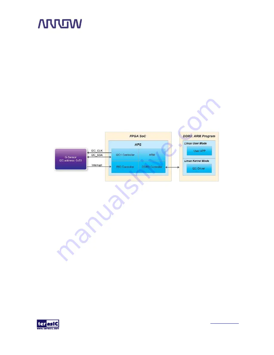
Function Block Diagram 

Figure 6-8 

s

hows the function block diagram of this demonstration. The G-sensor on the SoCKit 

board is connected to the 

I2C1

 controller in HPS. The G-Sensor I2C 7-bit device address is 0x53. 

The system I2C bus driver is used to access the register files in the G-sensor. The G-sensor interrupt 
signal is connected to the PIO controller. In this demonstration, we use polling method to read the 
register data, so the interrupt method is not introduced here. 


Figure 6-8 Block Diagram of the G-sensor Demonstration


I2C Driver 

Here is the list of procedures in order to read a register value from G-sensor register files by using 
the existing I2C bus driver in the system: 

5.


Open I2C bus driver "/dev/i2c-1": file = open("/dev/i2c-1", O_RDWR);   

6.


Specify G-sensor's I2C address 0x53: ioctl(file, I2C_SLAVE, 0x53); 

7.


Specify desired register index in g-sensor: write(file, &Addr8, sizeof(unsigned char)); 

8.


Read one-byte register value: read(file, &Data8, sizeof(unsigned char)); 


Because the G-sensor I2C bus is connected to the I2C1 controller, as shown in the 

Figure 6-9

, the 

given driver name is '/dev/i2c-1'.   


Summary of Contents for SoCKit

Page 1: ...SoCKit User Manual 1 www terasic com December 1 2015...

Page 2: ...rd Setup Components 11 3 1 1 JTAG Chain and Setup Switches 11 3 1 2 FPGA Configuration Mode Switch 13 3 1 3 HPS BOOTSEL and CLKSEL Setting Headers 14 3 1 4 HSMC VCCIO Voltage Level Setting Header 16 3...

Page 3: ...9 128x64 Dots LCD 44 3 7 10LTC Connector 45 CHAPTER 4 SOCKIT SYSTEM BUILDER 47 4 1 Introduction 47 4 2 General Design Flow 47 4 3 Using SoCKit System Builder 48 CHAPTER 5 EXAMPLES FOR FPGA 53 5 1 Aud...

Page 4: ...SoCKit User Manual 3 www terasic com December 1 2015 CHAPTER 7 STEPS OF PROGRAMMING THE QUAD SERIAL CONFIGURATION DEVICE 88 CHAPTER 8 APPENDIX 96 8 1 Revision History 96 8 2 Copyright Statement 96...

Page 5: ...seamlessly with the FPGA fabric using a high bandwidth interconnect backbone The SoCKit development board includes hardware such as high speed DDR3 memory video and audio capabilities Ethernet network...

Page 6: ...er reference designs and device datasheets User can download this System CD form the link http sockit_support terasic com 1 1 3 3 G Ge et tt ti in ng g H He el lp p For discussion support and referenc...

Page 7: ...chapter presents the features and design characteristics of the board 2 2 1 1 L La ay yo ou ut t a an nd d C Co om mp po on ne en nt ts s A photograph of the board is shown in Figure 2 1 and Figure 2...

Page 8: ...users to implement a wide range of designed circuits from simple circuits to various multimedia projects The following hardware is provided on the board F FP PG GA A D De ev vi ic ce e Cyclone V SoC 5...

Page 9: ...ith mini USB type AB connector USB to UART mini USB type B connector 10 100 1000 Ethernet C Co on nn ne ec ct to or rs s One HSMC 8 channel Transceivers Configurable I O standards 1 5 1 8 2 5 3 3V One...

Page 10: ...12V DC input 2 2 2 2 B Bl lo oc ck k D Di ia ag gr ra am m o of f t th he e S So oC CK Ki it t B Bo oa ar rd d Figure 2 3 gives the block diagram of the board To provide maximum flexibility for the us...

Page 11: ...SoCKit User Manual 10 www terasic com December 1 2015 Figure 2 3 Board Block Diagram...

Page 12: ...including JTAG chain HSMC I O voltage control HPS boot source select and others This section will explain the settings and functions in detail 3 3 1 1 1 1 J JT TA AG G C Ch ha ai in n a an nd d S Se...

Page 13: ...igure 3 1 The JTAG chain on the board Figure 3 2 JTAG Chain and Setup Switches Table 3 1 SW4 JTAG Control DIP Switch Board Reference Signal Name Description Default SW4 1 JTAG_HPS_EN On Bypass HPS Off...

Page 14: ...ring the FPGA via the EPCQ256 the SoCKit will be unable to boot Linux from the SD card or other devices Please switch SW6 to another mode e g MSEL 4 0 00001 to enable normal operations of Linux Figure...

Page 15: ...X4 Enabled Disabled Enabled Fast 10010 Standard 10011 3 3 1 1 3 3 H HP PS S B BO OO OT TS SE EL L a an nd d C CL LK KS SE EL L S Se et tt ti in ng g H He ea ad de er rs s The processor in the HPS can...

Page 16: ...1 Short Pin 2 and 3 Logic 0 Short Pin 1 and 2 J15 CLKSEL0 Short Pin 1 and 2 Logic 1 Short Pin 2 and 3 Logic 0 Short Pin 2 and 3 J16 CLKSEL1 Short Pin 1 and 2 Logic 1 Short Pin 2 and 3 Logic 0 Short Pi...

Page 17: ...onnector s default standard is 2 5V Users must ensure that the voltage standards for both the main board and daughter card are the same or damage incompatibility may occur Table 3 6 lists JP2 settings...

Page 18: ...wer is active TXD UART TXD Illuminates when data from FT232R to USB Host RXD UART RXD Illuminates when data from USB Host to FT232R D9 HSMC PSNTN Illuminates when connecting a daughter card on HSMC co...

Page 19: ...and USB OTG device Active low input that will reset all HPS logics that can be reset Places the HPS in a default state sufficient for software to boot KEY6 HPS_WARM_RST_n Warm reset to the HPS block A...

Page 20: ...nfiguration device chip into the FPGA when the board is powered up To program the configuration device users will need to use a Serial Flash Loader SFL function to program the quad serial configuratio...

Page 21: ...Before programming the quad serial configuration device please set the FPGA configuration mode switch SW6 to ASx4 mode 3 3 5 5 C Cl lo oc ck k C Ci ir rc cu ui it ts s Figure 3 10 is a diagram showing...

Page 22: ...ed using a Schmitt Trigger circuit as indicated in Figure 3 12 The four outputs called KEY0 KEY1 KEY2 and KEY3 of the Schmitt Trigger devices are connected directly to the Cyclone V SoC FPGA Each push...

Page 23: ...ovides a low logic level to the FPGA and when the switch is in the UP position it provides a high logic level Figure 3 13 Connections between the slide switches and Cyclone V SoC FPGA There are also f...

Page 24: ...2 PIN_AC28 Slide Switch 2 2 5V SW 3 PIN_AC29 Slide Switch 3 2 5V Table 3 10 Pin Assignments for Push buttons Signal Name FPGA Pin No Description I O Standard KEY 0 PIN_AE9 Push button 0 3 3V KEY 1 PI...

Page 25: ...ts and inputs high speed serial I O transceivers and single ended or differential signaling Signals on the HSMC port are shown in Figure 3 15 Table 3 12 shows the maximum power consumption of the daug...

Page 26: ...IN_AC2 Transceiver RX bit 1 1 5 V PCML HSMC_GXB_RX_p 2 PIN_AA2 Transceiver RX bit 2 1 5 V PCML HSMC_GXB_RX_p 3 PIN_W2 Transceiver RX bit 3 1 5 V PCML HSMC_GXB_RX_p 4 PIN_U2 Transceiver RX bit 4 1 5 V...

Page 27: ...I O Depend on JP2 HSMC_RX _n 14 PIN_E13 LVDS RX bit 14n or CMOS I O Depend on JP2 HSMC_RX _n 15 PIN_G13 LVDS RX bit 15n or CMOS I O Depend on JP2 HSMC_RX _n 16 PIN_F14 LVDS RX bit 16n or CMOS I O Depe...

Page 28: ...epend on JP2 HSMC_TX _p 5 PIN_E3 LVDS TX bit 5 or CMOS I O Depend on JP2 HSMC_TX _p 6 PIN_E4 LVDS TX bit 6 or CMOS I O Depend on JP2 HSMC_TX _p 7 PIN_C3 LVDS TX bit 7 or CMOS I O Depend on JP2 HSMC_TX...

Page 29: ...C Chip Clock 3 3V AUD_BCLK PIN_AE7 Audio CODEC Bit Stream Clock 3 3V AUD_I2C_SCLK PIN_AH30 I2C Clock 3 3V AUD_I2C_SDAT PIN_AF30 I2C Data 3 3V AUD_MUTE PIN_AD26 DAC Output Mute Active Low 3 3V 3 6 4 VG...

Page 30: ...ed by the display interval c During the data display interval the RGB data drives each pixel in turn across the row being displayed Finally there is a time period called the front porch d where the RG...

Page 31: ...4 2 0 6 56 XGA 60Hz 1024x768 2 1 2 5 15 8 0 4 65 XGA 70Hz 1024x768 1 8 1 9 13 7 0 3 75 XGA 85Hz 1024x768 1 0 2 2 10 8 0 5 95 1280x1024 60Hz 1280x1024 1 0 2 3 11 9 0 4 108 Table 3 16 VGA Vertical Timin...

Page 32: ...3 3V VGA_B 0 PIN_AE28 VGA Blue 0 3 3V VGA_B 1 PIN_Y23 VGA Blue 1 3 3V VGA_B 2 PIN_Y24 VGA Blue 2 3 3V VGA_B 3 PIN_AG28 VGA Blue 3 3 3V VGA_B 4 PIN_AF28 VGA Blue 4 3 3V VGA_B 5 PIN_V23 VGA Blue 5 3 3V...

Page 33: ...The board supports 1GB of DDR3 SDRAM comprising of two x16 bit DDR3 devices on FPGA side The DDR3 devices shipped with this board are running at 400MHz if the hard external memory interface is enable...

Page 34: ...DDR3_BA 2 PIN_AK11 DDR3 Bank Address 2 SSTL 15 Class I DDR3_CAS_n PIN_AH7 DDR3 Column Address Strobe SSTL 15 Class I DDR3_CKE PIN_AJ21 Clock Enable pin for DDR3 SSTL 15 Class I DDR3_CK_n PIN_AA15 Clo...

Page 35: ...DDR3_DQ 29 PIN_AE22 DDR3 Data 29 SSTL 15 Class I DDR3_DQ 30 PIN_AG25 DDR3 Data 30 SSTL 15 Class I DDR3_DQ 31 PIN_AK27 DDR3 Data 31 SSTL 15 Class I DDR3_DQS_n 0 PIN_W16 DDR3 Data Strobe n 0 Differenti...

Page 36: ...re 3 21 shows the connections between temperature sensor and Cyclone V SoC FPGA Table 3 20 gives the all the pin assignments of the sensor Figure 3 21 Connections between FPGA and Temperature Sensor T...

Page 37: ...24 Input only HPS_SW 0 GPI7 GPIO2 20 Input only HPS_SW 1 GPI6 GPIO2 19 Input only HPS_SW 2 GPI5 GPIO2 18 Input only HPS_SW 3 GPI4 GPIO2 17 Input only HPS_LED 0 GPIO54 GPIO1 25 I O HPS_LED 1 GPIO55 GP...

Page 38: ...MII transmit data 3 3 3V HPS_ENET_RX_DV PIN_K17 GMII and MII receive data valid 3 3V HPS_ENET_RX_DATA 0 PIN_A21 GMII and MII receive data 0 3 3V HPS_ENET_RX_DATA 1 PIN_B20 GMII and MII receive data 1...

Page 39: ...t support HW flow control signals The physical interface is done using UART USB onboard bridge from an FT232R chip and connects to the host using a Mini USB B connector For detailed information on ho...

Page 40: ...I HPS_DDR3_A 10 PIN_D29 HPS DDR3 Address 10 SSTL 15 Class I HPS_DDR3_A 11 PIN_C30 HPS DDR3 Address 11 SSTL 15 Class I HPS_DDR3_A 12 PIN_B30 HPS DDR3 Address 12 SSTL 15 Class I HPS_DDR3_A 13 PIN_C29 H...

Page 41: ...L 15 Class I HPS_DDR3_DQ 27 PIN_T28 HPS DDR3 Data 27 SSTL 15 Class I HPS_DDR3_DQ 28 PIN_R27 HPS DDR3 Data 28 SSTL 15 Class I HPS_DDR3_DQ 29 PIN_R26 HPS DDR3 Data 29 SSTL 15 Class I HPS_DDR3_DQ 30 PIN_...

Page 42: ...e 3 24 Connections Between Cyclone V SoC FPGA and QSPI Flash Table 3 26 below summarizes the pins on the flash device Signal names are from the device datasheet and directions are relative to the Cycl...

Page 43: ...Data 3 3 3V 3 3 7 7 7 7 U US SB B 2 2 0 0 O OT TG G P PH HY Y The board provides USB interfaces using the SMSC USB3300 controller A SMSC USB3300 device in a 32 pin QFN package device is used to inter...

Page 44: ..._A14 Throttle the Data 3 3V HPS_USB_RESET_PHY PIN_G17 HPS USB PHY Reset 3 3V HPS_USB_STP PIN_C15 Stop Data Stream on theBus 3 3V 3 3 7 7 8 8 G G S Se en ns so or r The board is equipped with a digital...

Page 45: ...5 HPS I2C Data share bus 3 3V 3 3 7 7 9 9 1 12 28 8x x6 64 4 D Do ot ts s L LC CD D The board equips an LCD Module with 128x64 dots for display capabilities The LCD module uses serial peripheral inter...

Page 46: ...t 3 3V 3 3 7 7 1 10 0 L LT TC C C Co on nn ne ec ct to or r The board allows connection to interface card from Linear Technology The interface is implemented using a14 pin header that can be connected...

Page 47: ...scription I O Standard HPS_LTC_GPIO PIN_F16 HPS LTC GPIO 3 3V HPS_I2C_CLK PIN_H23 HPS I2C Clock share bus with G Sensor 3 3V HPS_I2C_SDA PIN_A25 HPS I2C Data share bus with G Sensor 3 3V HPS_SPIM_CLK...

Page 48: ...situations that are prone to errors when users manually edit the top level design file or place pin assignments The common mistakes that users encounter are the following 1 Board damage due to wrong...

Page 49: ...erface Figure 4 1 The general design flow of building a design 4 4 3 3 U Us si in ng g S So oC CK Ki it t S Sy ys st te em m B Bu ui il ld de er r This section provides the detailed procedures on how...

Page 50: ...4 2 The SoCKit System Builder window Input Project Name Input project name as show in Figure 4 3 Project Name Type in an appropriate name here it will automatically be assigned as the name of your to...

Page 51: ...mponent is enabled the SoCKit System Builder will automatically generate the associated pin assignments including the pin name pin location pin direction and I O standard Figure 4 4 System Configurati...

Page 52: ...er card assigned in your design Users may leave this field empty Project Setting Management The SoCKit System Builder also provides functions to restore default setting loading a setting and saving us...

Page 53: ...4 1 The files generated by SoCKit System Builder No Filename Description 1 Project name v Top level Verilog HDL file for Quartus II 2 Project name qpf Quartus II Project File 3 Project name qsf Quartu...

Page 54: ...ry contains no spaces otherwise the Nios II software will not work Note Quartus II v13 is required for all SoCKit demonstrations to support Cyclone V SoC device 5 5 1 1 A Au ud di io o R Re ec co or r...

Page 55: ...uartus II The hardware part includes all the other blocks The AUDIO Controller is a user defined Qsys component It is designed to send audio data to the audio chip or receive audio data from the audio...

Page 56: ...t board Connect a speaker or headset to LINE OUT port on the SoCKit board Load the bit stream into FPGA note 1 Load the Software Execution File into FPGA note 1 Configure audio with the Slide switches...

Page 57: ...the microphone in line in and line out ports on the SOCKIT board to create a Karaoke Machine application The SSM2603 audio CODEC is configured in the master mode with which the audio CODEC generates A...

Page 58: ...output of a music player such as an MP3 player or computer to the line in port blue color on the SOCKIT board Connect a headset speaker to the line out port green color on the SOCKIT board Load the b...

Page 59: ...SoCKit User Manual 58 www terasic com December 1 2015 Figure 5 4 Setup for the Karaoke Machine...

Page 60: ...the entire memory space of the DDR3 through the Avalon interface of the controller In this project the Avalon bus read write test module will first write the entire memory and then compare the read b...

Page 61: ...the batch file folder SoCKit_DDR3_RTL_Test demo_batch Press KEY0 on the SoCKit board to start the verification process When KEY0 is pressed the LEDs LED 2 0 should turn on At the instant of releasing...

Page 62: ...refreshed at appropriate intervals System Block Diagram Figure 5 6 shows the system block diagram of this demonstration The system requires a 50 MHz clock provided from the board The DDR3 controller...

Page 63: ...by clicking Quartus menu Tools TCL Scripts Design Tools Quartus II 13 1 Nios II Eclipse 13 1 Demonstration Source Code Quartus Project directory SoCKit_DDR3_Nios_Test Nios II Eclipse SoCKit_DDR3_Nios_...

Page 64: ...as shown in Figure 5 7 Figure 5 7 Display Progress and Result Information for the DDR3 Demonstration 5 5 5 5 I IR R R Re ec ce ei iv ve er r D De em mo on ns st tr ra at ti io on n In this demonstrat...

Page 65: ...displayed in nios2 terminal Figure 5 9 shows the block diagram of the design Figure 5 8 Terasic Remote controller Table 5 4 Key code information for each Key on remote controller Key Key Code Key Key...

Page 66: ...e remote controller is pressed the remote controller will emit a standard frame shown in Figure 5 10 The beginning of the frame is the lead code represents the start bit and then is the key related in...

Page 67: ...ock will change the state from IDLE to GUIDANCE once the Lead code is detected Once the Code Detector has detected the Custom Code status the current state will change from GUIDANCE to DATAREAD state...

Page 68: ...oCKit_IR elf D De em mo on ns st tr ra at ti io on n S Se et tu up p F Fi il le e L Lo oc ca at ti io on ns s a an nd d I In ns st tr ru uc ct ti io on ns s Make sure Quartus II and Nios II are instal...

Page 69: ...st tr ra at ti io on n This demonstration illustrates how to use the ADT7301 device with the Nios II Processor to realize the function of board temperature detection Figure 5 15 shows the system block...

Page 70: ...os2 terminal window in order to let the user monitor the board real time temperature Figure 5 15 Block diagram of the Temperature Demonstration D De em mo on ns st tr ra at ti io on n S So ou ur rc ce...

Page 71: ...installed on your PC Power on the SoCKit board Connect USB Blaster to the SoCKit board and install USB Blaster driver II if necessary Execute the demo batch file SoCKit _TEMP bat under the batch file...

Page 72: ...o install the demonstrations on your computer Copy the directory Demonstrations into a local directory of your choice Altera SoC EDS v13 1 is required for users to compile the c code project 6 6 1 1 H...

Page 73: ...aunch Altera SoC EDS Command Shell by executing C altera 13 1 embedded Embedded_Command_Shell bat Use the cd command to change the current directory to where the Hello World project is located Then ty...

Page 74: ...irst_hps is copied into the SD card under the home root folder in Linux Insert the booting micro SD card into the SoCKit board Power on the SoCKit board Launch PuTTY to connect to the UART port of Put...

Page 75: ...IO controller The registers can be accessed by application software through the memory mapped device driver which is built into Altera SoC Linux Figure 6 1 Block Diagram of GPIO Demonstration GPIO Int...

Page 76: ...ter the first bit controls the output value of first I O pin in the associated GPIO controller and the second bit controls the output value of second I O pin in the associated GPIO controller and so o...

Page 77: ...a specified register munmap clean up memory mapping close close device driver Developers can also use the following MACRO to access the register alt_setbits_word set specified bit value to zero for a...

Page 78: ...n direction of HPS_GPIO29 The bit 24 controls the pin direction of HPS_GPIO53 which connects to the HPS_LED0 the bits 25 controls the pin direction of HPS_GPIO54 which connects to the HPS_LED1 and so...

Page 79: ...32_t HW_REGS_MASK BIT_LED_ALL Switches and Keys Control Figure 6 6 shows the pin assignment of HPS users key and switch for the SoCKit board The controller pin HPS_GPI4 HPS_GPI11 are controlled by the...

Page 80: ...and so on In summary the input value of H_SW0 H_SW1 H_SW2 and H_SW3 are controlled by the bit 20 bit 19 bit 18 and bit 17 in the gpio_extra_porta register of the GPIO2 controller respectively The inp...

Page 81: ...1 Boot from SD card Make sure CLKSEL 1 0 00 Make sure MSEL 4 0 00001 Connect the USB cable to the USB to UART connector J4 on the SoCKit board and host PC Make sure the executable file hps_gpio is cop...

Page 82: ...errupt signal is connected to the PIO controller In this demonstration we use polling method to read the register data so the interrupt method is not introduced here Figure 6 8 Block Diagram of the G...

Page 83: ...t board The ADI ADXL345 G sensor provides user selectable resolution up to 13 bit 16g The resolution can be configured through the DATA_FORAMT 0x31 register In the demonstration we configure the data...

Page 84: ...B cable to the USB to UART connector J4 on the SoCKit board and host PC Make sure the executable file gsensor is copied into the SD card under the home root folder in Linux Insert the booting micro sd...

Page 85: ...ly three SPI signals LCM_SPIM_CLK LCM_SPIM_SS and LCM_SPIM_MOSI are required The LCM_D_C signal is used to indicate the signal transferred on the SPI bus is Data or Command When LCM_D_C signal is pull...

Page 86: ...Only SPI with clock rate 3 125MHz Please refer to the function LCDHW_Init in LCD_Hw c for details The header file socal alt_spim h which needs to be included into the SPI controller program defines a...

Page 87: ...e Code Build tool Altera SoC EDS v13 1 Project directory Demonstration SoC hps_lcd Binary file hps_lcd Build command make make clean to remove all temporary files Execute command hps_lcd Demonstration...

Page 88: ...SoCKit User Manual 87 www terasic com December 1 2015 Users should see the LCD displayed as shown in Figure 6 14 Figure 6 14 LCD display for the LCD Demonstration...

Page 89: ...ogramming files with the Quartus II software users need to generate a user specified SRAM object file sof which is the input file first Next users need to convert the SOF to a JIC file To convert a SO...

Page 90: ...o the JTAG Indirect Configuration File jic from the Programming file type field 3 In the Configuration device field choose EPCQ256 4 In the Mode field choose Active Serial X4 5 In the File name field...

Page 91: ...2015 Figure 7 2 Convert Programming Files Dialog Box 7 Click Add File 8 Select the SOF that you want to convert to a JIC file 9 Click Open 10 Highlight the Flash Loader and click Add Device See Figure...

Page 92: ...ember 1 2015 Figure 7 3 Highlight Flash Loader 12 Select the targeted FPGA that you are using to program the serial configuration device See Figure 7 4 13 Click OK The Convert Programming Files page d...

Page 93: ...elect Devices Page Figure 7 5 Convert Programming Files Page Write JIC File into Quad Serial Configuration Device To program the serial configuration device with the JIC file that you just created add...

Page 94: ...e to the Quartus II Programmer window i Choose Programmer Tools menu and the Chain cdf window appears ii Click Auto Detect and choose the device See Figure 7 6 iii Click the FPGA device and right clic...

Page 95: ...grammer window with one JIC file 3 Click Start to program serial configuration device Erase the Quad Serial Configuration Device To erase the existed file in the serial configuration device follow the...

Page 96: ...SoCKit User Manual 95 www terasic com December 1 2015 Figure 7 9 Erasing setting in Quartus II programmer window 5 Click Start to erase the serial configuration device...

Page 97: ...is st to or ry y Version Change Log V0 1 Initial Version Preliminary V0 2 Add CH5 and CH6 V0 3 Modify CH3 V0 4 Add CH6 HPS V1 0 Modify CH 7 V2 0 Modify Usb Connector QSPI Flash and CH7 8 8 2 2 C Co o...

Reviews: