Section 10—
DM 5010
DIAGRAMS
AND
CIRCUIT
BOARD
ILLUSTRATIONS
Symbols
Graphic
symbols and
class designation letters are
based on ANSI Standard Y32.2-1975.
Logic
symbology
is
based on ANSI Y32.14-1973 in
terms
of
positive logic. Logic symbols depict the logic
function performed
and may differ
from the manufac
turer's data.
The
overline
on a signal name indicates
that the signal
performs its intended function when
it is in the low state.
Abbreviations
are based on ANSI
Y1.1-1972.
Other ANSI standards that are used in
the preparation
of
diagrams
by Tektronix, Inc. are:
Y14.15, 1966
Y14.2,
1973
Y10.5,
1968
Drafting
Practices.
Line
Conventions and
Lettering.
Letter
Symbols for Quantities Used
in
Electrical Science
and Electrical
Engineering.
American
National
Standard Institute
1430
Broadway
New
York,
New York 10018
Component
Values
Electrical components
shown
on the diagrams are in
the following units unless noted otherwise:
Capacitors
=
Values one or greater are in picofarads (pF).
Values less than one are in microfarads
(
a
F).
Resistors
- Ohms (Ω).
The
information and special symbols below may appear in
this manual.-----------
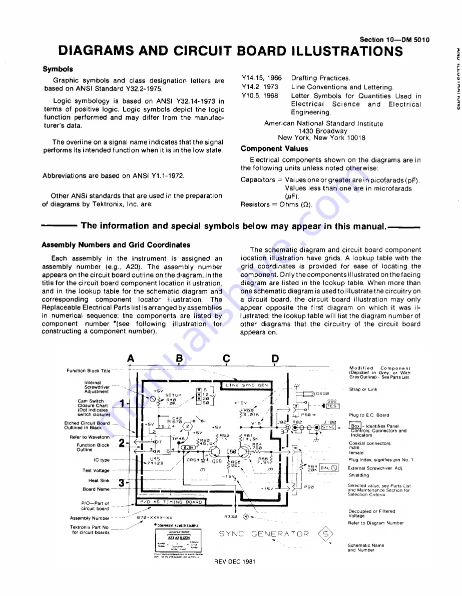
Assembly
Numbers and Grid Coordinates
Each
assembly
in the instrument is assigned an
assembly
number (e.g.,
A20). The assembly number
appears on the
circuit board outline on the diagram, in the
title for the circuit board component location
illustration,
and
in
the lookup table for the schematic diagram and
corresponding component
locator
illustration.
The
Replaceable
Electrical
Parts list isarranged by assemblies
in
numerical sequence; the components are listed by
component
number *(see following illustration for
constructing
a component
number).
The
schematic diagram and circuit board component
location
illustration have
grids. A lookup table with the
grid coordinates is provided for ease
of locating the
component. Only the components illustrated onthe
facing
diagram
are listed in the lookup table. When more than
one schematic diagram is
used
to illustrate the circuitry on
a
circuit
board, the circuit board illustration may
only
appear
opposite the first diagram on which it was il
lustrated;
the lookup table will list the diagram number of
other
diagrams
that
the circuitry
of the circuit board
appears
on.
Summary of Contents for DM 5010
Page 14: ...DM 5010 2994 00 DM 5010 Programmable Digital Multimeter xii ADD JUL 1986...
Page 27: ...Operating Instructions DM 5010 2994 03 Fig 2 3 DM 5010 front panel controls and connectors 2 3...
Page 38: ......
Page 134: ......
Page 208: ......
Page 222: ......
Page 250: ......
Page 251: ...Section 8 DM 5010 OPTIONS No options are available 8 1...
Page 252: ......
Page 270: ......
Page 272: ...DM 5010 2994 37 Fig 10 2 Location of DM 5010 adjustments and test points...
Page 273: ......
Page 274: ......
Page 275: ......
Page 276: ...DM 5010 2994 112 DM 5010 BLOCK DIAGRAM...
Page 281: ......
Page 282: ......
Page 291: ......
Page 293: ......
Page 294: ......
Page 297: ......
Page 298: ......
Page 303: ......
Page 304: ...I...
Page 305: ......
Page 310: ......
Page 311: ......
Page 315: ......
Page 318: ......
Page 321: ......
Page 323: ......
Page 326: ......
Page 332: ...2994 57...
Page 334: ......
Page 335: ......
Page 336: ......
Page 337: ...63 REV JUN 1986...
Page 338: ...FIG 1 EXPLODED DM 5010...
Page 339: ......
Page 340: ......
Page 341: ......
Page 347: ......