


Maintenance
—
DM 5010
Next,
check the
STROBE signal on the ADC and RMS
boards
at shift registers
U1500-1, diagram
2, and U1330-1,
diagram
3, respectively. The strobe should appear only dur
ing the short pulse at the end of the RD pulse train. Check
the
input and
output (pins
2 and 9) of
each register.
If
the shift
registers are working and a
range problem still
exists,
check
the latches
and the switches they drive for the
malfunction.
Refer
to Figs. 10-2
and 10-5 in the pullout
pages.
6.
A/D
CONVERTER, Isolation
Board, Diagram 5
First
determine whether
the
problem is
in the isolated or
grounded parts
of the A/D Converter. To do this, place the
Isolation
board
on one extender, leaving the top
board con
nector
unconnected. Jumper U1710-3 (U/D) to U1510-6
(COMP) on
the Isolation board. Check the display with U/D
jumpered
to COMP, an overrange
negative voltage indi
cates
the fault is in the isolated circuit; a displayed error
code 311 suggests the fault is
in the grounded circuit.
Re
move the
jumper between
U/D and COMP, and check the
indicated
circuit.
a. Isolated A/D Circuit: If the problem is
in the
isolated
section,
refer to the sections in the DC Voltage Measuring
Circuit
Troubleshooting section
dealing
with 311 errors and
the
Charge-Balancing Converter.
b. Grounded A/D
Circuit: Check the path of the TRIG
pulse
through the control ICs at the following points:
U1530A-6
(In Progress)
U1435C-8
U1425A-5
(M/2)
U1435A-3
U1330A-5 (Override)
U1230A-5
U1420C-8
U1425B-8
parallel representation of
the counters
inputs from U1020,
U1120,
U122Q, and U1130.
Trigger the oscilloscope on
U1425A-5, M/2,
diagram
5; then check that
the UP and
DOWN
pulses beginning at
U1020-5 and 4 propagate
through the counter ICs
and that their
outputs toggle appro
priately. Check that
the counter is reset to 0 by the RS
pulse,
U1020-11.
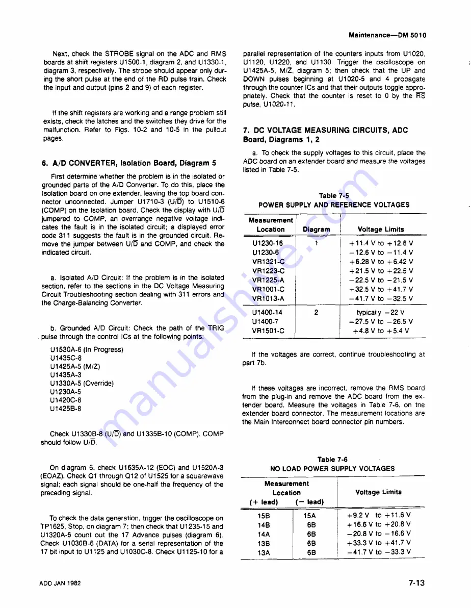
7.
DC VOLTAGE MEASURING CIRCUITS, ADC
Board, Diagrams 1, 2
a. To check the supply voltages to this circuit, place the
ADC board
on
an extender board and measure the voltages
listed in Table
7-5.
Table
7-5
POWER
SUPPLY AND REFERENCE VOLTAGES
Measurement
Location
Diagram
Voltage
Limits
U1230-16
1
+ 11.4Vto
+12.6 V
U
1230-6
-12.6 V to
-11.4V
VR1321-C
+
6.28 V to
+6.42 V
VR1223-C
+
21.5 V to
+22.5 V
VR1225-A
-22.5 V to
-21.5 V
VR1001-C
+
32.5 V to
+41.7 V
VR1013-A
-41.7 V to
— 32.5 V
U1400-14
2
typically
—
22 V
U1
400-7
-27.5 V to -26.5 V
VR1501-C
+4.8 V to
+5.4 V
If
the
voltages are correct, continue troubleshooting at
part 7b.
If
these
voltages
are incorrect,
remove the RMS board
from
the plug-in and remove the ADC board from the ex
tender
board.
Measure
the voltages in Table 7-6, on tne
extender
board connector.
The measurement locations are
the
Main Interconnect
board connector pin numbers.
Check
U1330B-8 (U/D)
and
U1335B-10 (COMP). COMP
should follow U/D.
On
diagram
6, check U1635A-12 (EOC) and U1520A-3
(EOAZ).
Check
Q1 through Q12 of U1525 for a squarewave
signal;
each signal should be one-half the frequency of the
preceding signal.
To check the data generation, trigger the oscilloscope
on
TP1625, Stop,
on diagram
7; then check that
U1235-15 and
U1320A-6 count
out the 17 Advance pulses (diagram 6).
Check
U1030B-6 (DATA) for a
serial representation of the
17 bit
input to U1125 and U1030C-8. Check U1125-10
for a
T
Table
7-6
NO LOAD
POWER
SUPPLY VOLTAGES
Measurement
Location
Voltage Limits
(+
lead)
(-
lead)
15B
15A
+
9.2 V to
+11.6 V
14B
6B
+ 16.6Vto
+20.8V
14A
6B
-20.8 V to
-16.6 V
13B
6B
+
33.3 V to
+41.7 V
13A
6B
-41.7 V to —
33.3 V
ADD
JAN
1982
7-13
Summary of Contents for DM 5010
Page 14: ...DM 5010 2994 00 DM 5010 Programmable Digital Multimeter xii ADD JUL 1986...
Page 27: ...Operating Instructions DM 5010 2994 03 Fig 2 3 DM 5010 front panel controls and connectors 2 3...
Page 38: ......
Page 134: ......
Page 208: ......
Page 222: ......
Page 250: ......
Page 251: ...Section 8 DM 5010 OPTIONS No options are available 8 1...
Page 252: ......
Page 270: ......
Page 272: ...DM 5010 2994 37 Fig 10 2 Location of DM 5010 adjustments and test points...
Page 273: ......
Page 274: ......
Page 275: ......
Page 276: ...DM 5010 2994 112 DM 5010 BLOCK DIAGRAM...
Page 281: ......
Page 282: ......
Page 291: ......
Page 293: ......
Page 294: ......
Page 297: ......
Page 298: ......
Page 303: ......
Page 304: ...I...
Page 305: ......
Page 310: ......
Page 311: ......
Page 315: ......
Page 318: ......
Page 321: ......
Page 323: ......
Page 326: ......
Page 332: ...2994 57...
Page 334: ......
Page 335: ......
Page 336: ......
Page 337: ...63 REV JUN 1986...
Page 338: ...FIG 1 EXPLODED DM 5010...
Page 339: ......
Page 340: ......
Page 341: ......
Page 347: ......


