background image

UP-5900VS

BIOS SETUP UTILITY

6 – 1

CHAPTER 6. BIOS SETUP UTILITY

1. OUTLINE

In UP-5900, there is a utility that rewrites minimum required setup infor-

mation at the system boot up that resides in ROM-BIOS.

Setup data is undefined at the first system startup, so setup must be
done. Basically, just doing initial setting in setup can do system opera-

tion.

Also, BIOS in UP-5900 will automatically detects memory size / HDD,

which makes no need for running setup again after changing hardware

(expanding memory, changing HDD, etc).

However, adding / removing second HDD will require running menu for-
mat setup.

2. STARTING PROCEDURE

There are 2 ways of starting setup, changing system SW and connect-

ing PS/2 type full keyboard. Setup started by each procedure will be as

follows.

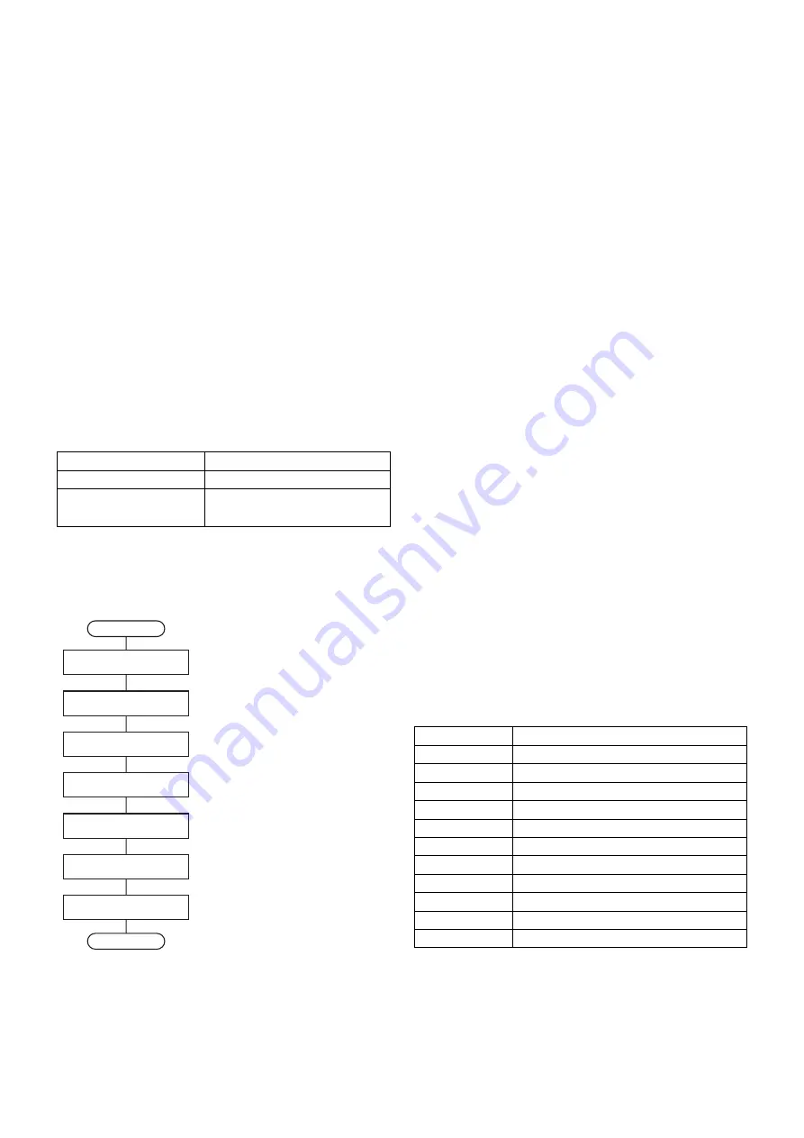
2-1. STARTING SETUP BY CHANGING SYSTEM SW

Setup data initialization will be processed when system is started with

system SW (JP2) turned on.

Following shows the flow of this procedure.

2-2. STARTING SETUP WITH FULL KEYBOARD

Starting and operating setup with full keyboard will require UP-C30PK,

PS/2 type full keyboard.

In this setup will use only numpad.

Procedure for starting setup is as follows.

(1) Start the system.

(2) On numpad, press period key when as following message appears

on screen.

“SETUP Available”

(3) If bios accepts above key, as following message appears on

screen.

“Entering SETUP...”

(4) Press following keys according to setup wanted while “Waiting

SETUP Entry Key ...” message appears on screen.

• Do setup initialization

3

 On numpad, press 8 and period at continuously.

Buzzer beeps 3 times and “CMOS Initialize Complete - Please

Restart.” message appears on screen. After this message, turn

off system power

•  Starting setup in menu format

3

 On numpad, press 7 and period at continuously.

After 1 beep, menu will be displayed. 

3. SETUP OUTLINE IN MENU FORMAT

Setup in menu format is not required during normal operation. Use only

in case such as checking contents of setup during maintenance, or

modifying setup contents required due to system operation.

3-1. KEY ASSIGNMENTS

Following num keys are used during operation of setup in menu format.

Setup in the menu format displays key assignment described in the

lower 2 lines. There is a case where [Continue] and [OK] are displayed

during help and in some settings. In this case, press arbitrary key to go
to next step.

Press period when [Press Enter] is displayed.

Procedure for running setup

Setup contents

Start with system SW

•  Setup data initialization.

Start with full keyboard

•  Setup data initialization. 

•  Running setup in menu format.

Start

Turn off system power

Change system SW (JP2)

to on position

Turn on system power

Buzzer beeps 3 times

Message displays notifying

initialization complete

Turn off system power

End

Change system SW (JP2)

to off position

; Always turn off power when 
  changing system SW

; "CMOS Initialize Complete - Please Restart."

; Setup data initialization complete

Key used

Functions

5

Display help

3 (Pg Dn)

Change setting (reverse)

9 (Pg Up)

Change setting (forward)

7 (Home)

Initialize all category displayed

1 (End)

Return to previous value

8 ( 

2

)

Change category (up)

2 (

 4

 )

Change category (down)

4 (

1

)

Change menu (left)

6 (

3

)

Change menu (right)

. (Del)

Select submenu, confirm, execute

0 (Ins)

End, return from submenu

Summary of Contents for UP-5900

Page 1: ...sed for after sales service only The contents are subject to change without notice UP5900VSME POS TERMINAL MODEL UP 5900 CHAPTER 1 SPECIFICATIONS 1 1 CHAPTER 2 OPTIONS 2 1 CHAPTER 3 SERVICE PRECAUTION 3 1 CHAPTER 4 DIAGNOSTICS SPECIFICATIONS 4 1 CHAPTER 5 CIRCUIT DESCRIPTION 5 1 CHAPTER 6 BIOS SETUP UTILITY 6 1 CHAPTER 7 HDI RECOVERY PROCEDURES 7 1 CHAPTER 8 ABOUT UTILITY SOFTWARE 8 1 CHAPTER 9 CI...

Page 2: ...LOW THE LOCAL RULES AND REGULATIONS BATTERY DISPOSAL THIS PRODUCT CONTAINS NICKEL METAL HYDRIDE BATTERY THIS BATTERY MUST BE DISPOSED OF PROPERLY REMOVE THE BATTERY FROM THE PRODUCT AND CONTACT FEDERAL OR STATE ENVIRONMENTAL AGENCIES FOR INFORMATION ON RECYCLING AND DISPOSAL OPTIONS TRAITEMENT DES ACCUMULATEUR USAGÉS CE PRODUIT CONTIENT UN ACCUMULATEUR À NICKEL MÉTAL HYDRIDE CET ACCUMULATEUR USAGÉ...

Page 3: ...ght pixels or blank pixels may appear Also an irregular color and brightness may occur depending on the view angle Please note that this type of phenomena is com mon for LCDs and may not be a malfunction The backlight in the display is a consumable part When the LCD display can no longer be adjusted and becomes darker you should replace the LCD module Consult your authorized SHARP dealer for furth...

Page 4: ... keys 11 keys 1 to 9 0 and 00 Capped keys 16 keys Key labels are locally purchased Maximum 30 keys 6x5 matrix Changing key layout by using ER 11KT7 12KT7 22KT7 Key layout ITEM SPECIFICATIONS NOTE CPU Celeron processor 566MHz Chip set Intel 440BX PIIX4e Graphic controller SMI Lynx3DM4 Main memory for executing MS DOS Application software Standard 128 Mbytes SD RAM Max 256 Mbytes adding DIMM Video R...

Page 5: ...ion is used to reset the stand by mode for power supply unit during software hang ups Release OFF Usually the shutdown switch needs to be set to this position when the UP 5900 is operating Shut down switch JP1 Setting of IRQ allocated to COM3 Position 1 2 COM3 IRQ4 2 3 COM3 IRQ11 JP2 Initialization of COMS Position 1 2 Initiallize 2 3 Not initiallize ON position Usually the power switch needs to b...

Page 6: ... Option for VK version UP C30PK Std 27 keys Max 30 keys 9 Key kit Used for key pad UP C30PK ER 11KT7 1 x 1 key top kit ER 12KT7 1 x 2 key top kit ER 22KT7 2 x 2 key top kit Incorporated in Main Unit RS 232 Communication Connection max 2 RS 232 Ethernet PC Keyboard Local item Drawer Option ER 03DW 04DW 05DW Customer Poll Displa Option UP P20DP Magnetic Card Reader Option UP E12MR2 Additional DRAM M...

Page 7: ...e from Terminal to Dongle 2 1 hole clerk key The key No 1 to No 12 are sup plied together with UP 5900 LKGIM1004BH13 BH Key No 13 LKGIM1004BH14 BH Key No 14 LKGIM1004BH15 BH Key No 15 LKGIM1004BH16 BH Key No 16 LKGIM1004BH17 BH Key No 17 LKGIM1004BH18 BH Key No 18 LKGIM1004BH19 BH Key No 19 LKGIM1004BH20 BH Key No 20 LKGIM1004BH21 BH Key No 21 LKGIM1004BH22 BH Key No 22 LKGIM1004BH23 BH Key No 23 ...

Page 8: ...004BH86 BH Key No 86 LKGIM1004BH87 BH Key No 87 LKGIM1004BH88 BH Key No 88 LKGIM1004BH89 BH Key No 89 LKGIM1004BH90 BH Key No 90 LKGIM1004BH91 BH Key No 91 LKGIM1004BH92 BH Key No 92 LKGIM1004BH93 BH Key No 93 LKGIM1004BH94 BH Key No 94 LKGIM1004BH95 BH Key No 95 LKGIM1004BH96 BH Key No 96 LKGIM1004BH97 BH Key No 97 LKGIM1004BH98 BH Key No 98 LKGIM1004BH99 BH Key No 99 No NAME PARTS CODE PRICE DES...

Page 9: ...agram 5 4 RS232 MODULAR JACK LOOP BACK CONNECTOR UKOG 6729BHZZ Connected to the RS232 connector RJ45 COM3 of the UP 5900 and used to check loop signals when executing diagnostics Connection diagram No NAME PARTS CODE PRICE DESCRIPTION 1 Parallel loop back connector UKOG 2366BHZZ BM 2 MCR test card UKOG 6718RCZZ BE for UP E12MR2 3 RS232 loop back connector UKOG 6705RCZZ BC for RS232 connector 4 RS2...

Page 10: ...ut around the air groove it may penetrate inside Be careful to keep the air groove away from water and oil Do not use sharp objects when making input entrees 4 NOTE FOR HANDLING OF LCD The LCD elements are made of glass BE careful not to expose them to strong mechanical shock or they may be broken Use extreme care not to break them If the LCD element is broken and the liquid leaks avoid contact wi...

Page 11: ...ish keyboard 101 keys Manufactured by NMB Technologies Inc Model RT6651T 7 PRECAUTION FOR ATTACHING THE COVER TO THE POWER UNIT When attaching the cover to the power unit two lead wires white x 1 black x 1 of T1A transformer in the power unit may be pinched by the cover causing a damage to the wiring 1 To avoid this push two lead wires of T1A between the radiator fin and T1A before attaching the c...

Page 12: ...ng band through the core as shown in the photo Procedure 2 Bind the core as shown in the photo and pull the band to fix Procedure 3 Fix so that the binding position of the band does not extend out of the plate Binding position of the binding band Inside The binding position of the band must be inside of this position Core RCORF2356BHZZ SC18E Pass all the cables 1pin 15pin through the core SC18E ex...

Page 13: ... 2 Sequential Seek Test 4 11 3 Random Seek Test 4 11 4 Seek Read Test 4 12 5 Target Sector Read Test 4 12 6 HD Dump Test 4 13 7 Error lnformation Display 4 13 8 Controller check Test 4 14 WRITE MODE TEST 4 14 9 Seek Write Read Verify Test 4 14 10 Target Sector Write Read Verify Test 4 15 11 HD Patch Test Utility 4 15 12 Error Logging Area Clear 4 15 13 Error table display 4 15 14 Other Supplementa...

Page 14: ...d data are compared by each word If it is O K test data 5555H is written to the test area iv Test data 0000H is written to all the test areas v Test data and read data are compared by each word If it is O K test data FFFFH is written to the test area vi Test data and read data are compared by each word If it is O K test data 0000H is written to the test area When an error occurs during the test th...

Page 15: ...ollows i Test address data is saved to the main memory ii Test data 55H is written to the test address iii Test data and read data are compared and test data AAH is written to the test address iv Test data and read data are compared v The saved test data is written to the test area vi The address is incremented until it becomes 3FH If POFF interruption is generated during the test the test is stop...

Page 16: ...te and return to the Touch panel diagnostics menu 2 TOUCH KEY PAD TEST 1 Checking content The driver function call is used The is displayed at the four corners of the LCD sequentially In the sequence of upper right upper left lower left lower right When the is touched by the operator the buzzer sounds and the screen turns to 2 Display 3 Terminating method Touch all four areas or press the Esc key ...

Page 17: ...orts standard provision 2 Display 3 Terminating method Press the Esc key to terminate and return to the Printer diagnostics menu 2 PARALLEL Print Check 1 Checking content The print check is performed for the standard port PARALLEL at I O address 378H 37FH In the print check mode the D Sub 25 pin connector is connected with a printer to allow a print pattern test The test procedures are as follows ...

Page 18: ...RJ45 port connect the loop back connector UKOG 6729BHZZ Loop back connector UKOG 6705RCZZ wiring diagram Loop back connector UKOG 6729BHZZ wiring diagram The UP 5900 s 9 pin D sub ports are used as COM1 and 2 The UP 5900 also provides a RJ45 port is used as COM3 The following menu is displayed The highlighted cursor is moved by the cursor keys UP 2 and DOWN 4 of the PS2 keyboard Move the cursor to...

Page 19: ...rminate and return to the Serial I O diagnos tics menu 2 COM2 CHECK 1 Checking content The loop back check is performed for the UART at I O address 2F8H 2FFH The check procedure the display and the terminat ing method are the same as COM1 Check 3 COM3 CHECK 1 Checking content The loop back check is performed for the UART at I O address 3E8H When the RJ 45 port of the UP 5900 main unit is assigned ...

Page 20: ...ser vice diagnostics menu HHHHHHHHHHHHHHHHHHHHHHHHHHHHHHHHHHHHHHHHHHHHHHHHHHHHHHHHHHHHHHHHHHHHHHHHHHH HHHHHHHHHHHHHHHHHHHHHHHHHHHHHHHHHHHHHHHHHHHHHHHHHHHHHHHHHHHHHHHHHHHHHHHHHHH HHHHHHHHHHHHHHHHHHHHHHHHHHHHHHHHHHHHHHHHHHHHHHHHHHHHHHHHHHHHHHHHHHHHHHHHHHH HHHHHHHHHHHHHHHHHHHHHHHHHHHHHHHHHHHHHHHHHHHHHHHHHHHHHHHHHHHHHHHHHHHHHHHHHHH HHHHHHHHHHHHHHHHHHHHHHHHHHHHHHHHHHHHHHHHHHHHHHHHHHHHHHHHHHHHHHHHHHHHHH...

Page 21: ...nformation of the main PWB is displayed Pressing the Esc key returns to the service diagnostics menu 1 SYSTEM SWITCH 1 Checking content The system switch reads I O address 7F0H every 10ms to display the value of bit 7 6 0 The relationship between the bit and JP switch is as shown in the table below Reference only not for diagnostics 2 Display Each JP switch data is displayed at X If the bit data i...

Page 22: ...ed ii The test pattern with all digits ON is displayed iii All OFF 2 Display 3 Terminating method Press the Esc key to turn off the VFD display and terminate the test Return to the Option display diagnostics menu and the test is termi nated 3 16 IDE I F HARD DISK DIAGNOSTICS The hard disk is tested and the information stored in the hard disk is dis played The following tests are executed Read test...

Page 23: ... test is started 3 Terminating method Press the Esc key during execution of the test or during interruption of the test to terminate the test and return to the above menu screen 3 RANDOM SEEK TEST Test condition setting Same as the above sequential read However execution of the test by 1 Pass means execution of random seek through the set cylinder range 1 Checking content The random seek is execut...

Page 24: ...g method The methods to interrupt resume and terminate the test are the same as 2 Sequential read 5 TARGET SECTOR READ TEST Test conditions setting Cylinder range 0 inmost cylinder The cylinder range to be tested is set Head count 0 final head The head umber to be tested is set Sector count 0 final sector The sector number to be tested is set Retry count 0 4 Retry number incase of an error is set ...

Page 25: ... to return to the menu screen of previous 1 7 ERROR INFORMATION DISPLAY 1 Checking content Error information stored in the inmost area of the HDD is displayed When the hard disk test is executed error information stored in the error information storing area is displayed The inmost cylinder 0 head and 1 sector 6 sector are read to be displayed 2 Display Every time the Enter key is pressed the next ...

Page 26: ...fferent data from the original stored data Before writing or reading the head is moved to the previous or the following cylinder Head movement When track N is read the head moves as follows The head arm is deflected back and forth In the direction of 0 3 inmost cylinder Writing is made at 2 Reading is made at 2 and 4 In the direction of 0 1 inmost cylinder Writing is made at 2 Reading is made at 2...

Page 27: ...inating method Same as test 6 12 ERROR LOGGING AREA CLEAR 1 Checking content The last cylinder area in the HD is cleared with 00H Error logging area last cylinder all sectors of 0 head The areas to be cleared with 00H is the last cylinder and all the sec tors of 0 head 2 Display Select Yes at position move with the 1 key and press the Enter key to execute the test When the test is executed once th...

Page 28: ...CS 1 FAN LCD ON OFF CHECK 1 Checking content The CPU the fan the exhaust fan and the LCD are turned ON OFF When this menu is selected the following display is shown When any key is pressed the CPU fan and the exhaust fan are stopped and the LCD and the backlight are turned off When any key is pressed under this state or if there is no key input for 10 sec the display automatically returns to the m...

Page 29: ...h the PS2 key board as follows A RSET8139 A is the DOS prompt Used by the FD Do not load any device drivers when using this program To operate other applications after performing this program re boot the machine SELECTION MENU The Diagnostics menu is started and the following menu is displayed The high lighted cursor is moved by the cursor keys UP 2 and DOWN 4 of the PS2 keyboard Move the cursor t...

Page 30: ...the MAC address of the UP 5900 PG8139 EXE and 8139C CFG configuration file are required The MAC address must be written after NoteID on the first line of 8139C CFG by using a text editor The lower 6 digits of the MAC address is indicated on the seal attached as shown in Fig 4 The upper 6 digits 08 00 1F is common to all the units Do not load any device drivers when using this program To operate ot...

Page 31: ...0 u2 Use 1 port SM Bus Support Real Time Clock 256byte Battery Back up CMOS SRAM AGP PCI Interface Use AGP u1 Video memory 4Mbyte Display Support DSTN and TFT panel support up to 1280 u 1024 SXGA FDC Enable Serial Port 16C550 compatible with Infrared u2 Parallel used for LPT1 BIOS ROM Bank Control Fixed 2 banks UART u5 8250 compatible COM 5ch Clocked Serial I O u2 CKDC I F Mode Switch Sense 16 bit...

Page 32: ...e VGAC Lynx3DM4 PSC2 Ultra I O PC87309 BIOS ROM KBC M38813 M010 PCI bus ISA bus AGP bus GTL IDE Clock Generator LVDS Analog Touch Panel 3 5 FDD 8MHz HDD Serial1 Serial2 COM1 COM2 LPT1 PS 2 Keyboard POS key PAD System SW Serial3 Serial6 COM3 5 Serial4 COM4 6 UP T80BP UP P20DP UP I20D Clerk SW 7 37MHz Driver Drawer MCR LANC RTL8139C RJ 45 USB Port 1 PS 2 I SA SLOT 1 1 ...

Page 33: ...SA I O 00 0F DMA ch0 3 control 400 40A 10 1F System 40B EISA DMA Extended Mode control 20 21 Master 8259 Interrupt control 410 4EF 22 24 Chipset Configuration 4D6 EISA DMA Extended Mode control 40 43 Timer control 4D7 57F 48 4B Timer control 580 59F POS I O 50 52 System 5A0 7EF 60 6F Keyboard Mouse control 7F0 7F1 PSC Special System Register 70 7F RTC CMOS RAM Index Data 7F2 7FF 80 8F DMA Page Reg...

Page 34: ...e Control 3E8 3EF COM3 control 3F0 3F7 FD HD control 3F8 3FF COM1 control Address Standard I O Option I O Address Legacy ISA I O Address POS I O 180 189 Extended Interrupt control o 18A Drawer control o 18B 18F Timer Counter control o 190 191 CSIO1 CKDC control RSVD 192 193 CSIO2 CKDC control RSVD 194 BIOS Bank control o 195 ROM RAM Disk Base Address RSVD 196 197 Interrupt Status Read o 198 199 Ma...

Page 35: ...RQ12 Mouse PCI ISA KBC PCI ISA KBC PCI IRQ13 Coprocessor u u u IRQ14 Primary IDE HDC HDC HDC IRQ15 Secondary IDE Serial7 Serial7 3 4 IRQx Touch Panel IRQ3 COM2 Serial2 Serial2 COM2 COM4 u Serial4 u Serial4 u IRQ4 COM1 Serial1 Serial1 COM1 COM3 u Serial3 u Serial3 u IRQ5 LPT2 ISA ISA PCI IRQ6 FDC FDC FDC FDC IRQ7 LPT1 LPT1 LPT1 LPT1 Extended Interrupt On Board POS Device IRQx0 MCR For UP E12MR E12M...

Page 36: ...Q1 IRQ5 PIRQ3 PIRQ4 PIRQ10 PIRQ11 IRQ9 IRQ15 IRQ3 IRQ4 IRQ10 IRQ11 IRQ10 IRQ11 IRQ3 IRQ4 IRQ6 IRQ7 IRQ5 IRQ12 IRQ12 IRQ1 IRQ1 DIRQ INTA INTB INTC INTD IRQ15 IRQ10 IRQ11 IRQ12 IRQ14 PIRQA PIRQB PIRQC PIRQD 5V 2 7K 2 7K 2 7K 10K 1K 5V 5V 5V 5V 5V 10K 5V 10K 5V 10K 10K 10K 10K 10K 5V 3 3V 3 3V 3 3V 3 3V 10K 5V 0 0 0 0 0 0 22 No Mount ...

Page 37: ... 0000h AD11 440BX Host to PCI Bridge 0001h 0000h AD12 PCI to PCI Bridge 0007h 0000h AD18 PIIX4e PCI to ISA Bridge 0001h IDE Interface 0002h USB Interface 0003h Power Management 000Ah 0000h AD21 RTL8139C LAN Controller 0012h XXXXh AD29 PCI SLOT Expansion SLOT 1 0000h 0000h AD16 Lynx3DM4 VGA AGP connection Master Device No Request allow signal Device Device 0 REQ0 GNT0 Not Used Device 1 REQ1 GNT1 No...

Page 38: ...of RESET the processors sample the A 31 3 pins to determine their power on configuration A20M I If the A20M Address 20 Mask input signal is asserted the Intel Celeron processor masks physical address bit 20 A20 before looking up a line in any internal cache and before driving a read write transaction on the bus Asserting A20M emulates the 8086 processor s address wrap around at the 1MB boundary As...

Page 39: ...t provides AGTL edge control and should be pulled up to VCCCORE with a 51 Ω m 5 resistor NOTE This signal is NOT used on the FC PGA package EMI S E P P only I EMI pins should be connected to motherboard ground and or to chassis ground through zero ohm 0 Ω resistors The zero ohm resistors should be placed in close proximity to the Intel Celeron processor connector The path to chassis ground should ...

Page 40: ...ation of the processors PWRGOOD I The PWRGOOD Power Good signal is a 2 5 V tolerant processor input The processor requires this signal to be a clean indication that the clocks and power supplies VCCCORE etc are stable and within their specifications Clean implies that the signal will remain low capable of sinking leakage current without glitches from the time that the power supplies are turned on ...

Page 41: ...tely 135 C This is signaled to the system by the THERMTRIP Thermal Trip pin Once activated the signal remains latched and the processor stopped until RESET goes active There is no hysteresis built into the thermal sensor itself as long as the die temperature drops below the trip level a RESET pulse will reset the processor and execution will continue If the temperature has not dropped below the tr...

Page 42: ... MD60 MD28 MD29 MD61 R VCC VSS VCC MD25 MD26 MD57 MD58 MD27 T MD59 MD54 MD24 MD23 MD55 MD56 U VCC MD51 MD52 VSS MD53 MD22 V VSS MD50 MD18 MD19 MD21 MD20 W VCC MECC7 MD48 MD16 MD17 MD49 Y SRASB VCC VSS VCC VSS DQMA6 MECC2 DQMA7 MECC6 MECC3 AA CSA0 VSS MAA1 MAB3 MAB6 MAB7 MAB10 DCLKO NC CSB5 VSS VSS DQMA3 AB DQMA5 CSA3 MAB1 MAA3 MAA7 MAA8 MAB9 MAA12 CKE0 CKE4 CSB3 DQMA2 CSB4 AC DQMB5 CSA4 MAB0 MAB2 ...

Page 43: ...a Bus ECC Parity Enhanced data bus integrity IERR Internal Error Direct internal error observation via IERR pin INIT Soft Reset Implemented by PIIX4E BIST supported by external logic BERR Bus Error Unrecoverable error without a bus protocol violation RP Request Parity Parity protection on ADS and PREQ 4 0 RSP Response Parity Signal Parity protection on RS 2 0 Name Type Description Name Type Descri...

Page 44: ...DO SDRAM These signals carry Memory ECC data during access to DRAM Name Type Description Name Type Description AD 31 0 I O PCI PCI Address Data These signals are connected to the PCI address data bus Address is driven by the 82443BX with FRAME assertion data is driven or received in the following clocks When the 82443BX acts as a target on the PCI Bus the AD 31 0 signals are inputs and contain the...

Page 45: ... register Any ECC errors received during initialization should be ignored The 82443BX asserts SERR for one clock when it detects a target abort during 82443BX initiated PCI cycle The 82443BX can also assert SERR when a PCI parity error occurs during the address or data phase The 82443BX can assert SERR when it detects a PCI address or data parity error on AGP The 82443BX can assert SERR upon detec...

Page 46: ...sistor ADSTB_B I O AGP AD Bus Strobe B This signal is an additional copy of the AD_STBA signal This signal requires an 8 2K ohm exter nal pull up resistor SBSTB I AGP Sideband Strobe THis signal provides timing for a side band bus This signal requires an 8 2K ohm external pull up resistor AGP FRAME Protocol SIgnals similar to PCI 2 GFRAME I O AGP Graphics Frame Same as PCI Not used by AGP GFRAME r...

Page 47: ...nce It feeds an external buffer clock device that produces multiple copies for the DIMMs DCLKWR I CMOS SDRAM Write Clock Feedback reference from the external SDRAM clock buffer This clock is used by the 82443BX when writing data to the SDRAM array PCIRST I CMOS PCI Reset When asserted this signal will reset the 82443BX logic All PCI output and bi directional signals will also tri state compliant t...

Page 48: ...During subsequent clocks AD 31 0 contain data A PIIX4E Bus transaction consists of an address phase followed by one or more data phases Little endian byte ordering is used AD 7 0 define the least significant byte LSB and AD 31 24 the most significant byte MSB When PIIX4E is a Target AD 31 0 are inputs during the address phase of a transaction During the following data phase s PIIX4E may be asked t...

Page 49: ... negated by PIIX4E PIIX4E implements the passive release mechanism by toggling PHOLD inactive for one PCICLK During Reset High Z After Reset High During POS High PHLDA I PCI HOLD ACKNOWLEDGE An active low assertion indicates that PIIX4E has been granted use of the PCI Bus Once PHLDA is asserted it cannot be negated unless PHOLD is negated first SERR I O SYSTEM ERROR SERR can be pulsed active by an...

Page 50: ...an input when an ISA master other than PIIX4E owns the ISA Bus This signal is also driven by PIIX4E during refresh cycles For DMA cycles PIIX4E as a master asserts MEMR During Reset High Z After Reset High During POS High MEMW I O MEMORY WRITE MEMW is the command to a memory slave that it may latch data from the ISA data bus MEMW is an output when PIIX4E owns the ISA Bus MEMW is an input when an I...

Page 51: ...set High During POS High RCIN I RESET CPU This signal from the keyboard controller is used to generate an INIT signal to the CPU RTCALE GPO25 O REAL TIME CLOCK ADDRESS LATCH ENABLE RTCALE is used to latch the appropriate memory address into the RTC A write to port 70h with the appropriate RTC memory address that will be written to or read from causes RTCALE to be asserted RTCALE is asserted on fal...

Page 52: ...eneral purpose output During Reset High After Reset High During POS High GPO APICCS GPO13 O APIC CHIP SELECT This active low output signal is asserted when the APIC Chip Select is enabled and a PCI orig inated cycle is positively decoded within the programmed I O APIC address space If the external APIC is not used this pin is a general purpose output During Reset High After Reset High During POS H...

Page 53: ...nected to the ignore numeric exception pin on the CPU IGNNE is only used if the PIIX4E coprocessor error reporting function is enabled If FERR is active indicating a coprocessor error a write to the Coprocessor Error Register F0h causes the IGNNE to be asserted IGNNE remains asserted until FERR is negated If FERR is not asserted when the Coprocessor Error Register is written the IGNNE signal is no...

Page 54: ...Type Description PDA 2 0 O PRIMARY DISK ADDRESS 2 0 These signals indicate which byte in either the ATA command block or control block is being addressed If the IDE signals are configured for Primary and Secondary these signals are connected to the corresponding sig nals on the Primary IDE connector If the IDE signals are configured for Primary 0 and Primary 1 these signals are used for the Primar...

Page 55: ...igh During POS High Z PIORDY I PRIMARY IO CHANNEL READY In normal IDE mode this input signal is directly driven by the corresponding IDE device IORDY signal In an Ultra DMA 33 read cycle this signal is used as STROBE with the PIIX4E latching data on rising and falling edges of STROBE In an Ultra DMA 33 write cycle this signal is used as the DMARDY signal which is negated by the drive to pause Ultr...

Page 56: ...econdary this signal is connected to the corresponding signal on the Secondary IDE connector If the IDE signals are configured for Primary Master and Primary Slave these signals are used for the Primary Slave connector During Reset High After Reset High During POS High SDIOW O SECONDARY DISK IO WRITE In normal IDE mode this is the command to the IDE device that it may latch data from the SDD 15 0 ...

Page 57: ...ernal Suspend Well power plane logic and portions of the RTC well logic SMBALERT GPI11 I SM BUS ALERT Input used by System Management Bus logic to generate an interrupt IRQ or SMI or power man agement resume event when enabled If this function is not needed this pin can be used as a general purpose input SMBCLK I O SM BUS CLOCK System Management Bus Clock used to synchronize transfer of data on SM...

Page 58: ...mode GPI1 GPI Non multiplexed GPI which is always available This signal when used by power management logic is active low GPI 2 4 REQ A C GPI GENCFG Bits 8 10 Not available as GPI if used for PC PCI Can be individually enabled so for instance GPI 4 is available if REQ C is not used GPI5 APICREQ GPI XBCS Bit 8 Not available as GPI if using an external APIC GPI6 IRQ8 GPI GENCFG Bit 14 Not available ...

Page 59: ...hich is always available Name Type Description CONFIG1 I CONFIGURATION SELECT 1 This input signal is used to select the type of microprocessor being used in the sys tem If CONFIG1 0 the system contains a Pentium microprocessor If CONFIG1 1 the system contains a Pentium II microprocessor It is used to control the polarity of INIT and CPURST signals CONFIG2 I CONFIGURATION SELECT 2 This input signal...

Page 60: ...then no sequencing requirements VSS V CORE GROUND These pins are the primary ground for PIIX4E VSS USB V USB GROUND This pin is the ground for the USB input output buffers Power Plane Description Signals Powered VCC Pins GND Pins RTC Contains the real time clock and 256 bytes of battery backed SRAM This plane is always powered if the internal RTC is used If the internal RTC is not used it may be c...

Page 61: ...SI2 KRTN2 14 P45 IRQ12 N U 39 P11 KSO9 N U 55 P31 KSI1 KRTN1 21 P40 xRC RCIN 40 P10 KSO8 N U 56 P30 KSI0 KRTN0 20 P41 GATEA20 A20GATE 41 P07 KSO7 N U 8 P53 HKO7 P U 25 P27 SCROLL N U 42 P06 KSO6 N U 9 P52 HKO6 P U 26 P26 NUM N U 43 P05 KSO5 KSTB5 10 P51 HKO5 P U 27 P25 APS N U 44 P04 KSO4 KSTB4 11 P50 HKO4 P U 28 P24 KANA PAD N U 45 P03 KSO3 KSTB3 29 P23 HKO3 P U 58 P61 TBDATA N U 46 P02 KSO2 KSTB...

Page 62: ...DD BE3 AD24 AD25 G MA7 MA3 MA4 VSS VSS SBA3 VDD AD26 AD27 AD28 H MA1 MA8 MA2 MA6 MA10 SBA2 VSS AD29 AD30 AD31 J SDCKEN SDCK MA9 MA0 VDD VSS VSS AVSS3 IREF2 SBA1 HVDD REQ GNT CLK K VCCA ROMEM DSF VCCA PME VSS VSS VSS AVDD3 SBA0 VSS RST INTA REFCLK L MD55 MD56 MD54 VSS VSS RS5 RS6 RS7 CVBS SB_STB MCKIN PDOWN CLKRUN EXCKEN M MD57 MD53 MD58 VCCA RS3 RS8 RS9 RS10 RS11 VSS PALCK VREF HREF BLANK N MD52 M...

Page 63: ...PDVWHU WR VWRS FXUUHQW WUDQVDFWLRQ HYLFH 6HOHFW Q 0 DVVHUWV WKLV VLJQDO ZKHQ LW GHFRGHV LWV DGGUHVVHV DV WKH WDUJHW RI WKH FXUUHQW WUDQVDFWLRQ 6HOHFW 7KLV LQSXW LV XVHG GXULQJ 3 FRQILJXUDWLRQ UHDG ZULWH F FOHV 6 VWHP ORFN 0 IRU 3 DQG 0 IRU 3 6 VWHP 5HVHW Q 0 DVVHUWV WKLV VLJQDO WR IRUFH UHJLVWHUV DQG VWDWH PDFKLQHV WR LQLWLDO GHIDXOW YDOXHV XV 5HTXHVW EXV PDVWHU PRGH XV UDQW EXV PDVWHU PRGH QWHUUX...

Page 64: ...HFW VW 0 ZLWKLQ WKH 0 PHPRU WHUQDO 6 5 0 2 PDVN 40 DUH E WH VSHFLILF 40 PDVNV 0 40 PDVNV 0 g DQG 40 PDVNV 0 WHUQDO 6 5 0 ORFN ZULWH WHUQDO 6 5 0 DQN 6HOHFW 6 5 0 KDV LQWHUQDO EDQNV DQN DGGUHVV GHILQHV WR ZKLFK EDQN WKH FXUUHQW FRPPDQG LV EHLQJ DSSOLHG WHUQDO 6 5 0 FORFN 6 LV GULYHQ E WKH PHPRU FORFN OO 6 5 0 LQSXW VLJQDOV DUH VDPSOHG RQ WKH SRVLWLYH HGJH RI 6 WHUQDO 6 5 0 FORFN HQDEOH 6 1 DFWLYDWH...

Page 65: ...H 7KLV VLJQDO LV XVHG WR FRQWURO ORJLF SRZHU ODW 3DQHO 9ROWDJH LDV QDEOH 7KLV VLJQDO LV XVHG WR FRQWURO LDV SRZHU 9 6 KDQQHO 2XWSXW 9 6 KDQQHO 2XWSXW 9 6 KDQQHO 2XWSXW 9 6 KDQQHO 2XWSXW 9 6 ORFN 2XWSXW QDORJ 5HG XUUHQW 2XWSXW QDORJ UHHQ XUUHQW 2XWSXW QDORJ OXH XUUHQW 2XWSXW XUUHQW 5HIHUHQFH QSXW 57 9HUWLFDO 6 QF 57 RUL RQWDO 6 QF RU RPSRVLWH 6 QF GHSHQGLQJ RQ 5 57 RUL RQWDO 6 QF RPSRVLWH 6 QF XPLQ...

Page 66: ...QWHUIDFH 9 RQ 2 5LQJ 9 9 6 3 3RZHU 6XSSO 9 9 6 3 URXQG 9 6 3RZHU 6XSSO 9 9 6 URXQG ORFN 3 QDORJ 3RZHU 9 QDORJ 3RZHU 9 79 QDORJ 3RZHU 9 5 0 LOWHUHG 3DOHWWH 3RZHU 9 3 QDORJ URXQG QDORJ URXQG QDORJ URXQG 79 QDORJ URXQG 5 0 LOWHUHG 3DOHWWH URXQG LJLWDO RUH 3RZHU 6XSSO 9 LJLWDO 0HPRU 3RZHU 6XSSO 9 9 RSWLRQ HVFULSWLRQ 3 2 SXOO GRZQ 3 2 SXOO XS 95 2 SXOO XS 5 2 SXOO XS 1 2 SXOO XS HQHUDO 3XUSRVH 5HJLVWHU...

Page 67: ...FL pin of the LT1184 In the UP 5900 VR1 on the main PWB is operated to change the current flowing between REF and ICCFL pin controlling the current flowing through the CCFL and adjusting the brightness VLOW VHIGH 10 6 COLOR GNDL GNDP 12V SHUTDOWN VR2 1 VR2 2 GND 5 1 4 3 2 R603A 2 2K CN502A 53015 0510 1 2 3 4 5 R502A 4 7K VR1 22K VR 1 3 2 F601A ICP0 5 CN501A SM02B BHSS 1 TB 2 1 R601A 100K C603A 100...

Page 68: ...is pulsed low by the printer to indicate that it has received data from the parallel port This pin is internally connected to an internal weak pull up AFD 74 Parallel Port I O Group 8 Automatic Feed When this signal is low the printer should automatically feed a line after printing each line This pin is in TRISTATE after a 0 is loaded into the correspond ing control register bit An external 4 7 KΩ...

Page 69: ...th information to control four FDDs when bit 7 of the SuperI O FDC Configuration register is 1 as described in Section 2 5 1 DR0 can optionally become a logical OR of DR0 and MTR0 when MTR0 DRATE0 is used as DRATE0 DR1 is multiplexed with DENSEL and is available only in Two UART mode Optionally it can become a logical OR of DR1 and MTR1 when MTR1 P12 is used as P12 DRATE0 95 45 or 43 FDC Output Gr...

Page 70: ...8 with RTS2 and ID1 and is available only in Full IR mode IRSL2 is multiplexed on pin 96 with DTR2 BOUT2 and ID2 and is available only in Full IR mode IRTX 44 UART2 Output Group 12 Infrared Transmit Infrared serial output data This signal is multiplexed with DENSEL only in Two UART mode KBCLK 59 KBC I O Group 6 Keyboard Clock This I O pin transfers the keyboard clock between the SuperI O chip and ...

Page 71: ...communications link peripheral device modem or other data transfer device The SOUT2 1 signals are set active high after a Master Reset MR SOUT2 is multiplexed on pin 100 with IRRX2 IRSL0 and ID0 and is available only in Two UART mode SOUT1 is multiplexed on pin 92 with CFG0 STB 67 Parallel Port I O Group 8 Data Strobe This output signal indicates to the printer that valid data is available at the ...

Page 72: ...e assigned to IRQ2 and UART1 can be assigned to IRQ4 PC X dedi cated interrupt IRQX can be assigned to IRQ9 UART1 2 and 5 can be assigned to IRQ10 and 11 UART1 2 and IRQX can be as signed to IRQ15 IRQX is a signal generated by taking OR among interrupt control from the POS dedicated device Assignment to each IRQ is controlled according to the setting of inter rupt assign register 0 and 1 IAR0 and ...

Page 73: ...re match signal can be generated and a maskable interrupt can be generated Also when TCNT1 is equal to TCC1 com pare match signal can be generated and a maskable interrupt can be generated When the TCNT0 overflows an overflow signal can be gen erated and a maskable interrupt can be generated Types of internal timer interrupt IS14 TINT0 timer compare match interrupt 0 IS13 TINT1 timer compare match...

Page 74: ... 114 113 112 111 110 109 108 107 106 105 1 2 3 4 5 6 7 8 9 10 11 12 13 14 15 16 17 18 19 20 21 22 23 24 25 26 27 28 29 30 31 32 33 34 35 36 37 38 39 40 41 42 43 44 45 46 47 48 49 50 51 52 157 158 159 160 161 162 163 164 165 166 167 168 169 170 171 172 173 174 175 176 177 178 179 180 181 182 183 184 185 186 187 188 189 190 191 192 193 194 195 196 197 198 199 200 201 202 203 204 205 206 207 208 104 ...

Page 75: ...6 RXD 49 O DTR2 RS 232 COM4 6 DTR 50 I DSR2 RS 232 COM4 6 DSR 51 O RTS2 RS 232 COM4 6 RTS 52 I CTS2 RS 232 COM4 6 CTS 53 I DCD2 RS 232 COM4 6 DCD 54 I RI2 RS 232 COM4 6 RI 55 GND 56 O TXD1 RS 232 COM3 5 TXD 57 I RXD1 RS 232 COM3 5 RXD 58 O DTR1 RS 232 COM3 5 DTR 59 I DSR1 RS 232 COM3 5 DSR 60 O RTS1 RS 232 COM3 5 RTS 61 I CTS1 RS 232 COM3 5 CTS 62 I DCD1 RS 232 COM3 5 DCD 63 I RI1 RS 232 COM3 5 RI...

Page 76: ...S SA22 155 I SA23 ISA BUS SA23 Pin No I O Signal name Function 156 GND 157 O PIRQ3 INTERRUPT REQUEST 3 to CPU 158 O PIRQ4 INTERRUPT REQUEST 4 to CPU 159 O PIRQ9 INTERRUPT REQUEST 8 to CPU 160 O PIRQ10 INTERRUPT REQUEST 10 to CPU 161 O PIRQ11 INTERRUPT REQUEST 11 to CPU 162 O PIRQ15 INTERRUPT REQUEST 15 to CPU 163 O PWRGD 164 GND 165 VDD 166 O PRAS0 STD PS RAM WORD CHIP SELECT 0 167 O PRAS1 OPT PS ...

Page 77: ... active low Used by the RTL8139C L to request a change in its current power management state and or to indicate that a power management event has occurred ISOLATEB ISOLATE I 95 Isolate pin Active low Used to isolate RTL8139C L from the PCI bus The RTL8139C L does not drive its PCI outputs excluding PME and does not sample its PCI input including RST and PCICLK as long as Isolate pin is asserted LW...

Page 78: ... Ready indicates the target agent s ability to complete the current phase of the transaction PAR T S 23 Parity is even parity across AD31 0 and C BE3 0 PERRB S T S 21 Parity Error When the RTL8139C L is the bus master and a parity error is detected the RTL8139C L asserts both SERR bit in ISR and Configuration Space command bit 8 SERRB enable Next it completes the current data burst transaction the...

Page 79: ...09 119 3 3V GND P 7 18 30 40 55 56 62 74 80 85 93 111 112 113 124 Ground Symbol Type Pin No Description LED0 1 2 O 99 98 97 LED pins LEDS1 0 00 01 10 11 LED0 TX RX TX RX TX TX LED1 LINK100 LINK10 100 LINK10 100 LINK100 LED2 LINK10 FULL RX LINK10 During power down mode the LED s are OFF Symbol Type Pin No Description TXD TXD O O 92 91 100 10BASE T transmit Tx data RXIN RXIN I I 87 86 100 10BASE T r...

Page 80: ...itsu control IC N010 0559 V021 Commands are given through the Serial Interface from the CPU Light Load Input Type Function OFF value 1 ON value 0 COM3 IRQ assign COM3 IRQ11 COM3 IRQ4 Function OFF value 1 ON value 0 CMOS Initialize Not Initialize Initialize Function OFF value 1 Serial3 decode mode COM3 SSR0 7 6 5 4 3 2 1 0 Read SW7 SW6 SW5 SW4 SW3 SW2 SW1 SW0 Write D7 D6 D5 D4 D3 D2 D1 D0 bit7 SW7 ...

Page 81: ... DIAG Self diag execution 89h 1 o u u SET TIME Timer setup after Pen Up 8Ah 1 o u u SET RATE Sampling interval setup 8Bh 1 o u u WRITE Write to E2PROM 8Ch 3 o u u READ Read from E2PROM 8Dh 1 o u o Reserve 8Eh Reserve 8Fh CALTRN Transmits the correction coefficient to CPU E0h 1 o u u CALRCV Transmits the correction coefficient to this controller E1h 170 o u o DUMY Dummy Data for Sleep Cancel FFh 0 ...

Page 82: ...ition the power is shut down PHOLD 1 Though Power Switch is at OFF position the power is kept on PHOLD Default is 0 To inhibit manual power OFF opera tion of Power Switch after POWER ON set to 1 When it is set to 0 the power can be turned off by manual operation of Power Switch This bit is designed for prevention of power OFF by manual operation of Power Switch and it has no effect on power interr...

Page 83: ...d end 1Fh 3Ah US n m Macro process execution 1Fh 5Eh n m US Self Test execution 1Fh 40h US v n Status check by DTR signal 1Fh 76h n US T n h m Counter Time setup and display 1Fh 54h n h m US U Counter Time display 1Fh 55h US n m Annunciater display select 1Fh 23h n m SLP Sleep Mode execution 06h n DC Select position display blinking 17h n m s US n Period display select 1Fh 2Eh n US n Comma display...

Page 84: ... the FIFO buffer Read from the main CPU is allowed by IN command of No Wait Even after reading the last character LCR the FIFO buffer has 10 20 characters of 0 Therefore when the last data LCR is read the FIFO should be reset before making the next card Read Enable In the MCR interface the next cars is not read until the interruption is reset from the main CPU 27 SERIAL PORT 27 1 OUTLINES D SUB 9p...

Page 85: ... and period at continuously Buzzer beeps 3 times and CMOS Initialize Complete Please Restart message appears on screen After this message turn off system power Starting setup in menu format 3 On numpad press 7 and period at continuously After 1 beep menu will be displayed 3 SETUP OUTLINE IN MENU FORMAT Setup in menu format is not required during normal operation Use only in case such as checking c...

Page 86: ...ly detected at BIOS boot up Serial port A Enabled Set enable disable on COM1 Serial port B Enabled Set enable disable on COM2 Parallel port Enabled Set enable disable on LPT1 Mode Bi Directional Set LPT1 Mode Can configurable Output only Bi Directional EPP ECP Use Bi Directional until announced by RETAILING SYSTEMS DEVELOPMENT DEPARTMENT Item Initial Value Description Note Boot Device Priority FD ...

Page 87: ...ification of any file in the UP 5900 Product Recovery CD ROM that is not described in this manual is forbidden SCSI or USB CD to be used must support DOS drivers Before executing recovery be sure to back up all necessary files to other media When recovery is executed all data in hard disk will be deleted When a SCSI device with bootable BIOS is used system will boot from SCSI device instead of UP ...

Page 88: ...t Recovery CD Utility is used all data in the HDD will be deleted Before executing recovery be sure to save the necessary files to other media 1 FD boot recovery Create a boot FD for recovery according to 5 Creating bootable FD for recoverying HDI Connect the keyboard and USB CD or SCSI CD drive to UP 5900 Insert bootable FD for recovery into FD drive of UP 5900 Turn on the power of UP 5900 When m...

Page 89: ... is no suspend to disk partition in UP 5900 HDI so 5 Recovering the suspend to disk partition will be skipped 5 When the Recovery CD Utility program is completed following message as shown below is displayed FD boot recovery Remove the UP 5900 Product Recovery CD ROM from CD drive and press Enter key to reboot from boot FD In the follow ing steps use only bootable FD and do not use UP 5900 Product...

Page 90: ...and After exiting from fdisk exe com mand press Ctrl Alt Del keys or turn UP 5900 power switch on off to reboot Since Fdisk exe program from Windows98 is used following mes sage will be displayed but please ignore the message Shut down Windows before restarting 13 When the machine is booted from boot FD or CD the recovery menu is displayed Use 2 4 keys to select 3 EXIT and press Enter key to go ba...

Page 91: ...p in order to run this utility Function The position calibration for the touch panel To adjust it use the touch pen of K PAD Keyboard enhanced Personal Digital Assistant PARTS CODE PARTS NAME MODEL CPENP1004PCN5 Touch pen K PDA ZR xxxx series File name DBLTAP EXE Out line Double tap setup utility DBLTAP EXE will call utility onward is used to improve double tap control over touch panel This utilit...

Page 92: ... Q3 2SD2444K B E C IC5D 74LVA08 TSSOP 12 13 11 14 7 F1 S2 R8 200 1 2 C28 220PF 2 1 C34 0 1UF 2125 2 1 C38 0 1UF 2 1 C457 220UF 10V OS R17 5 1K 1 2 R15 56 1 2 C31 0 022UF 2 1 C33 820PF 2 1 R16 82K 1 2 C12 1UF 2125 2 1 D4 SFPB54 C1 270UF 10V OS C13 1UF 2125 2 1 L3 2UH HK 15EER 20A01NC 3 4 2 1 D1 1SS355 A K IC6B 74LVA08 TSSOP 4 5 6 7 14 R9 22 2125 1 2 C7 0 1UF 2125 2 1 R2 10 1 2 IC6C 74LVA08 TSSOP 9 ...

Page 93: ... 0 1UF 2 1 C72 0 1UF 2 1 FB5 P121E 1 2 F B C62 56UF 10V rubycon ZAV C63 0 1UF 2 1 C64 0 1UF 2 1 C39 56UF 10V rubycon ZAV C51 0 1UF 2 1 C52 0 1UF 2 1 C44 0 1UF 2 1 C45 0 1UF 2 1 FB85 P121E 1 2 F B C69 0 1UF 2 1 C58 1UF 2125 2 1 C59 22UF LMK316F226ZL T 2 1 C74 1UF 2125 2 1 C75 1UF 2125 2 1 C42 0 1UF 2 1 FB2 P121E 1 2 F B C43 0 1UF 2 1 C76 1UF 2125 2 1 C77 1UF 2125 2 1 C73 0 1UF 2 1 C65 0 1UF 2 1 C66...

Page 94: ...1 2 R34 22 1 2 R45 0 1 2 C111 27PF 2 1 IC7 ICS9248 39 19 48 36 30 7 31 8 32 10 47 38 25 11 37 46 12 3 35 13 2 34 1 29 9 28 20 21 16 26 22 44 43 4 41 45 15 17 18 39 33 27 5 6 40 14 23 24 42 VDDSDRAM VDDIOAPIC VDDSDRAM VDDSDRAM MODE PCI_F SDRAM5 FS3 PCI0 SDRAM4 PCI1 IOAPIC SDRAM0 FS1 24MHz PCI2 SDRAM1 FS2 REF1 PCI3 GND SDRAM2 PCI4 PCI_STOP REF0 SDRAM3 VDDREF SDRAM6 GND SDRAM7 SDRAM9 SDRAM8 GND FS0 4...

Page 95: ...CN1 PZ37047 S01S AC1 A29 X6 AF4 AH4 W3 A31 E27 A33 X4 AN31 AC37 AJ31 AH14 AK24 AL11 C29 S35 C31 AN13 C33 AN17 E29 AN23 E31 AM2 B36 AL31 AH28 AH26 AL29 V4 AH22 AK28 X2 AN27 AH30 AK18 AK30 AJ35 AL33 AN25 AN35 AH16 AN37 AG35 AE33 AL25 AK32 AH18 AL23 AE35 AN33 F10 AL19 AG37 AL27 AG33 AL17 M36 AK20 L37 AK8 J33 AK26 J35 A35 L35 AN19 J37 AC35 AH12 AE37 AH8 G33 AN9 E37 AL15 AH10 W37 C35 AN29 E35 AL9 AH6 A...

Page 96: ...11 D24 AJ15 D28 AJ19 D32 AJ23 D36 AJ27 D6 AJ3 E13 AJ7 E17 AK36 E5 AK4 E9 AL1 F14 AL3 F2 AM10 F22 AM14 F26 AM18 F30 F34 AM22 F4 AM26 H32 AM30 H36 AM34 J5 AM6 K2 AN3 K32 B12 K34 B16 M32 B20 N5 B24 P2 B28 P34 B32 R32 B4 R36 B8 S5 D18 T2 D2 T34 D22 V32 D26 V36 D30 W5 D34 X34 D4 Y35 E11 Z32 E15 E19 E7 F20 F24 F28 F32 F36 G5 H2 H34 K36 L5 M2 M34 P32 P36 Q5 R34 T32 T36 U5 V2 V34 X32 X36 Y37 Y5 Z2 Z34 AG1...

Page 97: ...PF 2 1 R65 10K 1 2 IC12 440BX L24 K23 J26 L23 H26 H24 K21 B23 N23 G25 B22 H22 G23 D22 H23 G24 K25 K24 J23 J22 L25 L26 K26 B26 H25 K22 L22 E21 F26 G26 A22 G22 F22 D21 F23 J25 F24 C21 F25 E23 A21 E26 E25 C20 D25 D26 B21 B25 C26 E20 A25 C25 A20 A24 D24 E19 C23 B24 B20 C24 A23 E18 E22 D23 D20 D19 D18 C19 B19 A18 A19 B18 C17 E17 D17 B17 C16 A17 C15 B16 D16 A16 B15 A15 D14 D15 B13 C14 E14 D13 A13 D12 B1...

Page 98: ...AC13 AF23 AE15 AE24 AD25 AD23 AC15 AC25 AA17 AA10 AD15 AC23 AB26 AE16 AF24 AE14 AF17 AE25 AC14 AD24 AD26 AA22 AA23 AC24 AA26 AC26 AF11 AF12 AD12 AB23 AA25 AA24 Y22 AB16 AE13 AD14 AB13 AD10 AE12 AC12 AE17 AC17 AF4 AF18 AE19 AE10 AF19 AC18 AC19 AE20 AB11 AD20 AF21 AE4 AC21 AF25 AC11 Y23 AF5 Y26 W22 AD6 V22 V23 AE6 V25 U22 AB7 U25 U26 AC7 T24 T25 AF7 U21 R23 AB8 R26 P24 AB9 P25 AC9 AE9 AB10 AC10 AF10...

Page 99: ...49 150 151 153 154 155 156 158 159 160 161 1 12 23 32 43 54 64 68 78 85 96 107 116 127 138 148 152 162 6 18 26 40 41 49 59 73 84 90 102 110 124 133 143 157 168 33 117 34 118 35 119 36 120 37 121 38 122 39 123 126 132 115 111 28 29 46 47 112 113 130 131 21 22 52 53 105 106 136 137 27 30 45 128 42 125 79 163 165 166 167 82 83 24 25 50 51 61 63 80 81 108 109 134 135 145 147 31 44 48 62 146 114 129 16...

Page 100: ... C BE 0 12 29 30 C BE 3 12 29 30 SERR 12 29 30 FRAME 12 29 30 SDONE 30 SBO 30 IDSEL_VGA 32 IDSEL_LAN 29 INT _RISER0 12 30 INT _RISER1 INT _VGA 32 INT _LAN 29 REQ _RISER1 12 INTA INTD VCC3 VCC3 VCC3 VCC3 VCC3 VCC3 VCC3 JR11 0 23 1 3 2 BR41 8 2K 4 1 8 2 7 3 6 4 5 R95 47 1 2 R107 100 1 2 IC12C 440BX AB2 Y4 V4 W3 W5 V5 W4 Y1 L5 L3 Y2 L4 AB5 L2 J4 L1 AE2 K1 K6 M2 AD3 M1 G3 N2 AD2 P2 N5 P4 AD1 P3 E4 R1 ...

Page 101: ...3 R13 T14 R14 T16 R16 V6 R22 V21 T12 Y6 T15 Y21 V3 AA7 V24 AA9 W6 AA18 W21 AA20 AA6 AE1 AA8 AE26 AA19 AF2 AA21 AF14 AB3 AB12 AB15 AB24 AB25 AD5 AD9 AD18 AD22 AF1 AF13 AF26 AC4 VSS VDD VSS TESTIN VSS VDD VSS VSS VDD VSS NC SUSTAT VSS VDD VSS VSS VDD VSS BXPWROK VSS VDD VSS GTLREFA VSS VDD VSS GTLREFB VSS VDD VSS VTTA VSS VDD VSS VTTB VSS VDD VSS AGPREFV VSS VDD VSS PCIREF5V VSS VDD VSS NC VSS VDD V...

Page 102: ...9 30 PAR 10 29 30 C BE 3 10 29 30 SERR 10 29 30 C BE 2 10 29 30 STOP 10 29 30 IRDY 10 29 30 AD 0 31 10 29 30 INTD 30 INTA 30 VCC3 VCC3 VCC_CPU_CMOS IC13 PIIX4e L18 M19 E10 A1 L17 C1 L19 D2 L20 E1 M20 D4 K19 A11 J18 C6 P20 C8 K20 D1 A2 B11 B2 A5 C2 C5 C11 B5 E2 D5 B3 E5 C3 A6 E3 B6 D3 R3 A4 R4 B4 P5 C4 G1 E4 E6 A12 D6 B12 A7 A3 B7 C7 D7 A8 B8 E8 D8 A9 B9 C9 D9 A10 B10 B1 D11 INIT CPURST PCIREQA PCI...

Page 103: ...12 M11 J4 J5 R5 M16 M5 VCC VCC_RTC VCC VSS VCC VCC_SUS VCC VCC VCC_USB VCC VCC_SUS VCC VSS VCC VCC VREF VCC VSS VCC VCC VSS VCC NC VCC VSS VSS VSS VSS VSS VSS VSS VSS VSS VSS VSS VSS VSS NC VSS VSS NC VSS_USB NC NC NC TP29 FB17 1 2 F B C242 1UF 2125 2 1 C239 0 1UF 2 1 C243 1UF 2125 2 1 R118 1K 1 2 TP26 C241 0 1UF 2 1 D5 1SS355 A K C240 0 1UF 2 1 C238 1UF 2125 2 1 FB20 1 2 F B C254 1UF 2125 2 1 C25...

Page 104: ...047UF 2 1 TP51 R128 470 1 2 TP37 C484 220PF 2 1 TP47 TP33 BR53 2 7K 4 1 8 2 7 3 6 4 5 R101 0 1 2 BR51 8 2K 4 1 8 2 7 3 6 4 5 C472 0 1UF 2 1 BR52 2 7K 4 1 8 2 7 3 6 4 5 IC13C PIIX4e T20 N17 P16 U20 H19 P18 P19 P17 U18 V19 W20 V20 T18 M18 R1 R2 U19 M17 R19 Y20 V18 R17 R18 G4 C10 T17 M1 N2 P3 K18 L2 J3 L5 K3 K4 H1 H4 H5 G3 N1 P2 P4 J17 H18 H20 K2 L1 K1 K16 T19 G5 F2 F3 F4 N4 L4 N5 SMBDATA GPI11 SMBAL...

Page 105: ...7 A20GATE 27 VCC VCC VCC VCC VCC VCC VCC VCC VCC VCC3 VCC VCC3 VCC3 VCC C496 100PF 2 1 TP56 R138 2 7K 1 2 BR57 1K 4 1 8 2 7 3 6 4 5 R194 4 7K 1 2 C266 5PF 2 1 C267 10PF 2 1 X2 32 768KHz DT 26 R139 0 1 2 BR56 10K 8 EXBE10C103J 9 1 10 8 2 7 3 6 4 5 BR59 10K 4 1 8 2 7 3 6 4 5 C474 2 1 C265 2PF 2 1 R140 1M 1 2 TP55 1 TP57 BR54 10K 8 EXBE10C103J 9 1 10 8 2 7 3 6 4 5 TP298 C268 1000PF 2 1 BR63 10K 8 EXB...

Page 106: ...X4e A18 B17 G17 C17 G18 A16 C18 A17 D16 C16 B16 B18 D15 G16 F19 F18 H16 G19 G20 F17 F16 H17 C15 G2 A15 E17 E14 E19 B14 H3 D13 D17 B13 D19 D12 F1 C12 C19 A13 B19 C13 H2 A14 A19 C14 A20 D14 J1 B15 B20 E15 C20 J2 D20 D18 E20 E18 F20 L3 SIDE_A2 SIDE_A1 PIDE_A2 SIDE_A0 PIDE_A1 SIDE_DRQ SIDE_CS3J SIDE_AKJ SIDE_RDY SIDE_IORJ SIDE_IOWJ SIDE_CS1J SIDE_D15 PIDE_A0 PIDE_D15 PIDE_DRQ PIDE_CS3J PIDE_AKJ PIDE_R...

Page 107: ...C17F 74LVA04 TSSOP 13 12 14 7 C491 330PF 2 1 C492 330PF 2 1 CN5 IC160 0324 350 13 12 14 11 15 10 17 9 18 8 19 7 20 6 21 5 27 26 23 25 4 28 29 3 2 24 22 31 30 1 32 16 IO0 A0 IO1 A1 IO2 A2 IO3 A3 IO4 A4 IO5 A5 IO6 A6 IO7 A7 A8 A9 A10 A11 A12 A13 A14 A15 A16 OE CE WE A17 A18 VCC GND C272 22PF 2 1 C270 0 1UF 2 1 IC18 AT49F040 12JC 13 12 14 11 15 10 17 9 18 8 19 7 20 6 21 5 27 26 23 25 4 28 29 3 2 24 2...

Page 108: ...1 2 R175 0 R171 10 1 2 C291 0 1UF 2 1 C281 100PF 2 1 C282 100PF 2 1 C283 100PF 2 1 C284 100PF 2 1 C292 0 1UF 2 1 C285 100PF 2 1 R179 0 1 2 C286 100PF 2 1 C287 100PF 2 1 C288 100PF 2 1 C289 100PF 2 1 C297 270PF 2 1 R167 1K 1 2 C293 270PF 2 1 R170 1K 1 2 C298 270PF 2 1 R169 1K 1 2 C294 270PF 2 1 R184 0 1 2 R168 1K 1 2 C299 270PF 2 1 R166 1K 1 2 C295 270PF 2 1 C300 270PF 2 1 C296 270PF 2 1 C301 270PF...

Page 109: ...5 26 22 19 24 25 10 18 23 27 4 9 1 3 2 17 13 11 21 28 C1 C1 C2 C2 T1IN T2IN T3IN R1OUT R2OUT R3OUT R4OUT R5OUT EN SHDN GND R5IN R4IN R3IN R2IN R1IN T3OUT T2OUT T1OUT V V VCC T4IN T4OUT IC19B PC87309VLJ 89 99 92 88 86 83 100 85 84 98 87 96 93 95 94 97 SIN1 SIN2 ID3 SOUT1 CFG0 RTS1 BADDR1 DTR1 BADDR0 BOUT1 CTS1 SOUT2 IRSL0 IRRX2 ID0 DSR1 DCD1 RTS2 IRSL1 ID1 RI1 DTR2 BOUT2 IRSL2 ID2 CTS2 A11 DSR2 DRA...

Page 110: ...14 GIL G 12P S3T2 E 1 2 3 4 5 6 7 8 9 10 11 12 IC25C 74LS125 9 8 10 IC26A BA10393 3 2 1 8 4 FB26 BLM21 1 2 F B D10 IC24D 74LS125 12 11 13 FB27 BLM21 1 2 F B IC25D 74LS125 12 11 13 FB28 BLM21 1 2 F B IC25A 74LS125 2 3 1 IC26B BA10393 5 6 7 8 4 IC23 74HC138 1 2 3 6 4 5 15 14 13 12 11 10 9 7 A B C G1 G2A G2B Y0 Y1 Y2 Y3 Y4 Y5 Y6 Y7 D12 FB29 BLM21 1 2 F B D9 FB22 BLM21 1 2 F B D14 R202 3 3K CN15 53014...

Page 111: ...DS 26 12V VCC VCC 12V 12V Q10 DTA144EK 2 3 1 R205 6 8K R207 2 7K R209 1K R208 47K IC27A STA471A 2 3 1 CN17 5045 03A 2 1 3 FB33 BFR601009C8NG Q8 DTA144EK 2 3 1 C317 1000PF F3 400mA 250V CN16 5045 03A 2 1 3 C316 0 1UF FB32 BFR601009C8NG FB31 BFR601009C8NG IC27B STA471A 4 5 10 Q9 DTC114YK 2 3 1 Q7 DTC114YK 2 3 1 C315 0 1UF FB30 BFR601009C8NG R206 6 8K ...

Page 112: ...26 CLS2 26 RDD2 26 RCP2 26 VSS VDD PVCC5 VCC PVCC5 BR78 4 7K 4 1 8 2 7 3 6 4 5 CN18 5045 0810 1 2 3 4 5 6 7 8 IC28B 4069 3 4 FB37 BLM21 1 2 F B IC28C 4069 5 6 IC28D 4069 9 8 IC28A 4069 1 2 IC28E 4069 11 10 IC28F 4069 13 12 FB36 BLM21 1 2 F B FB39 BLM21 1 2 F B BR77 4 7K 2 1 4 2 3 BR80 10K 2 1 4 2 3 FB38 BLM21 1 2 F B FB35 BLM21 1 2 F B FB34 BLM21 1 2 F B BR79 10K 4 1 8 2 7 3 6 4 5 ...

Page 113: ...6 DTR5 26 RTS5 26 RXD5 26 DSR5 26 CTS5 26 VCC VPRN C318 100PF FB42 BLM21 1 2 F B FB43 BLM21 1 2 F B IC29A 74LV14A 1 2 FB45 BLM21 1 2 F B BR81 10K 4 1 8 2 7 3 6 4 5 CN19 53014 1010 1 2 3 4 5 6 7 8 9 10 IC29C 74LV14A 5 6 IC29D 74LV14A 9 8 C319 100PF IC29B 74LV14A 3 4 IC29E 74LV14A 11 10 IC29F 74LV14A 13 12 FB40 BLM21 1 2 F B C320 100PF FB44 BLM21 1 2 F B FB41 BLM21 1 2 F B ...

Page 114: ...4 0 1UF 2 1 C322 0 1UF 2 1 J1 JC 1 3 2 C323 0 1UF 2 1 IC47 HIN211 12 14 15 16 7 6 20 8 5 26 22 19 24 25 10 18 23 27 4 9 1 3 2 17 13 11 21 28 C1 C1 C2 C2 T1IN T2IN T3IN R1OUT R2OUT R3OUT R4OUT R5OUT EN SHDN GND R5IN R4IN R3IN R2IN R1IN T3OUT T2OUT T1OUT V V VCC T4IN T4OUT C433 0 1UF 2 1 CN33 53014 0910 1 2 3 4 5 6 8 9 7 IC30 HIN211 12 14 15 16 7 6 20 8 5 26 22 19 24 25 10 18 23 27 4 9 1 3 2 17 13 1...

Page 115: ...21 TM11R 3C 88 HIROSE 1 2 3 4 5 6 7 8 FB46 BLM21 1 2 F B IC31 HIN211 12 14 15 16 7 6 20 8 5 26 22 19 24 25 10 18 23 27 4 9 1 3 2 17 13 11 21 28 C1 C1 C2 C2 T1IN T2IN T3IN R1OUT R2OUT R3OUT R4OUT R5OUT EN SHDN GND R5IN R4IN R3IN R2IN R1IN T3OUT T2OUT T1OUT V V VCC T4IN T4OUT FB47 BLM21 1 2 F B C441 0 1UF 2 1 CN22 53014 0710 1 2 3 4 5 6 7 C439 0 1UF 2 1 C443 0 1UF 2 1 C440 0 1UF 2 1 C442 0 1UF 2 1 F...

Page 116: ... 19 20 21 22 23 24 25 65 66 67 68 69 166 167 168 169 170 171 173 174 175 176 177 178 179 180 181 184 185 186 187 188 189 190 191 56 57 58 59 60 61 62 63 47 48 49 50 51 52 53 54 28 29 30 31 32 33 34 35 37 38 39 40 41 42 43 44 85 86 87 88 89 90 91 92 71 72 73 74 75 76 77 80 81 82 83 84 94 95 96 97 98 99 27 46 78 110 130 165 182 Y737I Y737O BALE AEN MEMR MEMW IOR IOW MCS16 RESETDRV REFRESH IRQ3 IRQ4 ...

Page 117: ...DQ4 DQ3 DQ2 DQ1 DQ0 P17 P16 P15 P14 P13 P12 P11 P10 P07 P06 P05 P04 P03 P02 P01 P00 P37 P36 P35 P34 P33 P32 P31 P30 P27 P26 P25 P24 P44 P45 CNVSS VCC VSS P60 P46 P43 P47 P42 P40 P61 P20 XIN RES CS A0 RD WE P50 P51 P52 P53 P21 P22 P23 P41 XOUT IC34F 74HC04 13 12 C355 0 1UF X4 8MHz 1 3 2 C356 0 1UF CN25 1 2 3 4 5 6 VCC_USB DAT DAT GND_USB FRAME1 FRAME2 C357 0 1UF C350 56UF 10V rubycon ZAV C495 R343 ...

Page 118: ...VCC5 12V 12V 12V VCC5 PVCC5 C366 0 1UF Q15 DTC114YK 2 3 1 IC48 KIA78DL09F 2 3 1 IN OUT GND C361 47UF 25V CN28 5483 15AX 1 2 3 4 5 6 7 8 9 10 11 12 13 14 15 CN26 53014 0310 2 1 3 C438 0 1UF Q14 2SJ187 G D S F2 3 15A 250V C363 0 1UF C437 10UF 16V CN27 53014 0310 2 1 3 R335 5 6 1 2 C436 0 1UF C362 270UF 10V OS C360 47UF 25V C364 47UF 25V R237 10K C499 0 1UF 2 1 C365 47UF 25V ...

Page 119: ...M C367 0 1UF C374 15PF C381 0 1UF FB56 MPZ2012S101A R250 75 1 R364 0 R249 10K R245 10K IC46 M93C46 W 1 2 3 4 8 7 6 5 S C D Q VCC DU ORG VSS R251 75 1 LED3 LED R N M R247 1 8K U1 TLA 6T207 6 7 3 4 5 1 9 12 8 13 10 14 2 11 RD RD CT NC CT TD RX CT RX TX CT TX TD NC LED2 LED R N M R244 0 R254 51 1 1 LED1 LED R N M R253 51 1 1 R258 10K R243 1K CN29 TM11R 3C 88 1 2 3 4 5 6 7 8 C376 0 1UF C377 1000PF FB5...

Page 120: ...DONE 10 GNT _RISER0 10 PCIRST 15 17 26 27 INTD 10 12 INTA 12 VCC3 VCC3 12V PVCC5 PVCC5 12V CN30 20 5061 100 052 XXX 1 2 3 4 5 6 7 8 9 10 11 12 13 14 15 16 17 18 19 20 21 22 23 24 25 26 27 28 29 30 31 32 33 34 35 36 37 38 39 40 41 42 43 44 45 46 47 48 49 50 51 52 53 54 55 56 57 58 59 60 61 62 63 64 65 66 67 68 69 70 71 72 73 74 75 76 77 78 79 80 81 82 83 84 85 86 87 88 89 90 91 92 93 94 95 96 97 98...

Page 121: ...J16 N16 K16 E5 E10 P16 J9 D12 U5 E11 H20 E12 J10 E13 H19 K1 J11 E14 E15 E16 F16 G16 H16 N19 U9 U12 N18 K4 J17 K9 J19 L18 J20 P20 M4 L5 U15 K19 K12 D14 K10 U16 L19 D15 J18 P4 R5 D13 K11 K17 K20 T6 V15 P19 L4 V16 M16 D8 R17 K18 T5 D6 N4 A12 F5 D4 N17 D17 P18 F4 W16 A13 L20 Y17 F17 A14 Y19 T4 K5 A15 P5 M17 G17 A16 D5 A17 D10 D9 U18 R20 T7 D16 B12 E4 R19 B13 E17 A20 A18 D7 R18 G4 B15 A19 H17 B14 B16 C...

Page 122: ... FB89 C477 FB74 BLM21 3 TP1P 2 F4 ICP0 5 R347 22 1 2 C448 20PF VR2 200K VR 1 3 2 C450 15PF R317 22 1 2 C447 20PF R310 22 1 2 C449 20PF C451 15PF C430 0 1UF R370 0 FB86 R348 22 1 2 R296 20KF C464 TP2N 2 R294 10K R344 0 R311 22 1 2 C490 1UF 50V C446 20PF R349 22 1 2 Q17 SI9948DY 8 7 6 5 1 2 3 4 D1 D1 D2 D2 S1 G1 S2 G2 TP2P 2 R312 22 1 2 CN34 53047 1410 1 2 3 4 5 6 7 8 9 10 11 12 13 14 IC44A 74HCT08 ...

Page 123: ...2 H2 H4 F3 H5 F2 W2 W3 W4 Y4 V5 USR0 SCL USR1 SDA MA0 MCKIN LVDSCK BLUE MA9 SDCK RED CRTHSYNC MD4 IREF2 FDATA22 RS4 GREEN RS3 tx3n tx1p IREF tx0n tx2p MD5 tx1n CRTVSYNC FPSCLK SDCKEN FDATA23 txclkn FDATA19 FDATA16 FDATA13 FDATA8 FDATA5 MD55 FDATA2 MD56 MD54 tx3p tx0p tx2n RS9 ROMEN txclkp CVBS VBIASEN MD7 FDATA15 FDATA18 FDATA12 FDATA21 MD53 FDATA9 LP FHSYNC FDATA6 MD31 FDATA3 M DE FDATA0 DSF MD17...

Page 124: ...q HRESET ITPRST tck tms PRDY tdi tdo trst preq PRDY CLK_CPU VTT VTT CN601 146351 5 1 3 5 7 9 11 13 15 17 19 20 2 4 6 8 10 12 14 16 18 21 22 24 23 25 27 29 26 28 30 1 3 5 7 9 11 13 15 17 19 20 2 4 6 8 10 12 14 16 18 21 22 24 23 25 27 29 26 28 30 R603 47 1 2 R602 240 1 2 R605 240 1 2 R604 47 1 2 CN602 53047 1510 1 2 3 4 5 6 7 8 9 10 11 12 13 14 15 R601 1K 1 2 ...

Page 125: ...2 A23 A24 A25 A26 A27 A28 A29 A30 A31 A32 A33 A34 A35 A36 A37 A38 A39 A40 A41 A42 A43 A44 A45 A46 A47 A48 A49 A50 B1 B2 B3 B4 B5 B6 B7 B8 B9 B10 B11 B12 B13 B14 B15 B16 B17 B18 B19 B20 B21 B22 B23 B24 B25 B26 B27 B28 B29 B30 B31 B32 B33 B34 B35 B36 B37 B38 B39 B40 B41 B42 B43 B44 B45 B46 B47 B48 B49 B50 R15 22k R25 0 CN3 CON PCI HDC 120A 127D 2 3 4 5 9 11 12 13 16 18 19 20 21 22 23 24 25 26 27 28 ...

Page 126: ...0 0 1 2 3 4 5 6 7 8 9 10 11 12 13 14 15 16 17 18 19 20 21 22 23 24 25 26 27 28 29 30 C19 Ceramic C 0 1uF C12 4700pF FB3 BLM31 C18 18pF 2 1 R6 D12 Q1 DTA124EKA D1 1SS353 R16 100 CN101 000 6208 520 012 000 ELCO 1 2 3 4 5 6 7 8 9 10 11 12 C3 S101 KSP 04 1 2 3 4 8 7 6 5 C10 33uF 16V R9 1K C17 18pF 2 1 R8 R18 1k D2 1SS353 R3 D9 Q2 DTA124EKA D6 1SS353 C6 R10 8 2K C4 3300pFX2 IC2 S 29390AF E PROM 4 5 6 3...

Page 127: ...7K VR1 22K VR 1 3 2 F601A ICP0 5 CN501A SM02B BHSS 1 TB 2 1 R601A 100K C603A 1000pF C602A 1uF 16V C504A 22pF 3 15KV Q602A D2391 T501A 841TN 1157 C601A 0 082uF 100V IC501A LT1184 1 2 3 4 5 7 8 6 9 10 11 12 16 15 14 13 PGND ICCFL DIO VC AGND NC NC SHDN NC NC REF VIN VSW BULB BAT ROYER D602A SFPB54 C502A 22uF 16V Q601A D2391 C501A 2 2uF 50V L501A 100uH R604A 2 2K C503A 10uF 16V OS D601A SFPB54 R602A ...

Page 128: ...UP 5900VS PWB LAYOUT 10 1 CHAPTER 10 PWB LAYOUT MAIN PWB UPPER SIDE ...

Page 129: ...UP 5900VS PWB LAYOUT 10 2 BOTTOM SIDE ...

Page 130: ...UP 5900VS PWB LAYOUT 10 3 INVERTER PWB UPPER SIDE BOTTOM SIDE UPPER SIDE UPPER SIDE BOTTOM SIDE ...

Page 131: ...UP 5900VS PWB LAYOUT 10 4 UPPER SIDE BOTTOM SIDE UPPER SIDE BOTTOM SIDE ...

Page 132: ...2002 May Printed in Japan t COPYRIGHT 2002 BY SHARP CORPORATION All rights reserved Printed in Japan No part of this publication may be reproduced stored in a retrieval system or transmitted In any form or by any means electronic mechanical photocopying recording or otherwise without prior written permission of the publisher ...

Reviews: